EP0470646A2 - In situ-Messung einer dünnen Schicht auf einem Substrat - Google Patents
In situ-Messung einer dünnen Schicht auf einem Substrat Download PDFInfo
- Publication number
- EP0470646A2 EP0470646A2 EP91113471A EP91113471A EP0470646A2 EP 0470646 A2 EP0470646 A2 EP 0470646A2 EP 91113471 A EP91113471 A EP 91113471A EP 91113471 A EP91113471 A EP 91113471A EP 0470646 A2 EP0470646 A2 EP 0470646A2
- Authority
- EP
- European Patent Office
- Prior art keywords
- specimen
- emissivity
- radiation
- temperature
- layer
- Prior art date
- Legal status (The legal status is an assumption and is not a legal conclusion. Google has not performed a legal analysis and makes no representation as to the accuracy of the status listed.)
- Granted
Links
Images


Classifications
-
- G—PHYSICS
- G01—MEASURING; TESTING
- G01B—MEASURING LENGTH, THICKNESS OR SIMILAR LINEAR DIMENSIONS; MEASURING ANGLES; MEASURING AREAS; MEASURING IRREGULARITIES OF SURFACES OR CONTOURS
- G01B15/00—Measuring arrangements characterised by the use of electromagnetic waves or particle radiation, e.g. by the use of microwaves, X-rays, gamma rays or electrons
- G01B15/02—Measuring arrangements characterised by the use of electromagnetic waves or particle radiation, e.g. by the use of microwaves, X-rays, gamma rays or electrons for measuring thickness
Definitions
- the present invention relates to a method and apparatus for in situ monitoring and control of the thickness of a thin film during deposition in a wafer.
- polycrystalline silicon is deposited on oxidized silicon by chemical vapor deposition. It is important to accurately monitor and control the thickness of the layer of polycrystalline silicon as it is deposited. Typically this is done by complicated laser measurement system.
- the invention provides a method for monitoring the thickness of a layer deposited on top of a specimen according to independent claim 1, an apparatus for detecting the thickness of a layer deposited on a specimen according to independent claim 10 and a method for monitoring a process in which a layer is deposited on top of a specimen according to independent claim 17.
- a method and apparatus are presented for determining the thickness of a layer deposited on a specimen.
- the thickness of a layer of polycrystalline silicon may be measured as it is deposited over silicon oxide on a silicon wafer.
- the emissivity of radiation at the top of the silicon wafer is detected. This is done, for example, with one or more optical pyrometers.
- the emissivity varies with the thickness of the layer of polycrystalline silicon and with the temperature of the silicon wafer.
- the temperature of the silicon wafer is measured and the emissivity variation due to variation of the temperature is subtracted from the emissivity of radiation detected at the top of the wafer.
- the measurement of the temperature may be done, for example, by one or more optical pyrometers at the back of the wafer, or it may be done by a thermocouple. Once the emissivity variation due to variation of the temperature is subtracted, the resultant signal is used to calculate the thickness of the polycrystalline silicon layer.
- the present invention allows for the monitoring of the thickness of a layer of polycrystalline silicon at the time of deposition. This monitoring may be done despite variations in temperature during processing time.
- Figure 1 a cross-sectional view of a thermal reactor 11 used in chemical vapor deposition process.
- a layer of polycrystalline silicon is deposited upon a wafer 14.
- a wafer support structure 15 is used to support wafer 14.
- Wafer support structure 15 extends through a bottom aperture 16 of thermal reactor 11. This allows a drive assembly (not shown) to rotate wafer support structure 15 and thus wafer 14 during processing. This is done to enhance process uniformity.
- thermal reactor 11 During processing, gasses enter thermal reactor 11 through an entry port 12 and are removed through an exit port 13. Also during processing, heat is provided by infrared radiation bulbs, for example, an infrared radiation bulb 17, an infrared radiation bulb 18, an infrared radiation bulb 19 and an infrared radiation bulb 20.
- the infrared radiation bulbs are mounted on a support system 24 connected to housing 10.
- the walls of thermal reactor 11 are transparent allowing infrared radiation from the infrared radiation bulbs to freely enter thermal reactor 11 and heat wafer 14.
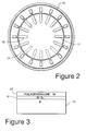
- Figure 2 shows a top cutaway view of infrared radiation bulbs including infrared radiation bulb 17 and infrared radiation bulb 18.
- infrared radiation bulb 17 and infrared radiation bulb 18.
- O7/491,416 entitled Double - Dome Reactor for Semiconductor Processing.
- a layer 61 of silicon oxide and a layer 62 of polycrystalline silicon may be deposited on silicon wafer 14.
- a typical thickness of layer 61 is 1000 Angstroms ** .
- a typical thickness of layer 62 is 3000 Angstroms, although layer 62 may typically range from 50 to 10,000 Angstroms.
- a certain amount of infrared radiation is absorbed by layer 61 and layer 62 and a certain amount is emitted.
- the amount of infrared radiation varies with the thickness of layer 62 and with the temperature of wafer 14.
- the amount of infrared radiation varies with the temperature of wafer 14.
- the radiation level at the top of wafer 14 and the radiation level at the bottom wafer 14 are measured. Using the measured level of infrared radiation it is possible to subtract out the change in infrared radiation from the top of wafer 14 resulting from variations in temperature. Once the subtraction has been performed, it is possible to determine the thickness of layer 62 based on the infrared radiation at the top of wafer 14.
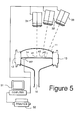
- Figure 4 shows an optical pyrometer 31 placed to measure emission of infrared radiation at a point 41 on top of wafer 14.
- An optical pyrometer 32 is placed to measure emission of infrared radiation at a point 42 on top of wafer 14.
- An optical pyrometer 33 is placed to measure emission of infrared radiation at a point 43 on top of wafer 14. While a single optical pyrometer may be used to measure emission of infrared radiation at the top of wafer 14, a plurality of optical pyrometers may be used when it is desirable to monitor deposition uniformity of layer 62 of polycrystalline silicon.
- an optical pyrometer 34 is placed to measure emission of infrared radiation at a point 44 on the bottom of wafer 14.
- An optical pyrometer 35 is placed to measure emission of infrared radiation at a point 45 on the bottom of wafer 14. While a single optical pyrometer may be used to measure emission of infrared radiation from the bottom of wafer 14, a plurality of optical pyrometers may be used when it is desirable to monitor temperature uniformity across wafer 14.
- Optical pyrometers 31-35 are, for example, able to measure temperature in the range of 500 degrees centigrade to 1250 degrees centigrade and detect a wavelength between two ⁇ m and four ⁇ m , for example 3.3 /1.m.
- Such an optical pyrometer is available from lrcon, Inc., having a business address of 7300 North Natchez Ave. Niles, Illinois 60648, or from Linear Labs, having a business address of 1290 Hammerwood Avenue, Sunnyvale, California 94089.
- Output of optical pyrometers 31-35 is received and evaluated by a computer 51.
- Computer 51 generates a current output which is converted to a voltage between zero and ten volts that is proportional to the temperature detected by optical pyrometers 31-35.
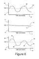
- Figure 6 shows a measured signal 64 plotted on a graph 60.
- Graph 60 has a horizontal axis 61 which represents the passage of time, and a vertical axis 62, which represents the temperature optical pyrometer 31, optical pyrometer 32 and/or optical pyrometer 33 measure at the top of wafer 14.
- a reference line 63 indicates a measured temperature of 700 degrees centigrade.
- Figure 6 also shows a measured signal 74 plotted on a graph 70.
- Graph 70 has a horizontal axis 71 which corresponds to the passage of time as represented by horizontal axis 61 of graph 60.
- Graph 70 also has a vertical axis 72, which represents the temperature optical pyrometer 34 and/or optical pyrometer 35 measure at the bottom of wafer 14.
- a reference line 73 indicates a measured temperature of 700 degrees centigrade.
- Graph 80 has a horizontal axis 81 which corresponds to the passage of time as represented by horizontal axis 61 of graph 60 and horizontal axis 71 of graph 70.
- a vertical axis 82 represents the measured radiation emitted from the top of wafer 14 which is not caused by changes in temperature.
- a reference line 83 is also shown.
- Calculated temperature differential signal 84 may be used to monitor the thickness of layer 62 at processing time.
- calculated temperature differential signal 84 may be generated for a specific process. Parameters of the process may include, for example, type of oxide film deposited, pattern in which a deposit is made, the deposition rate, temperature of deposit and the pressure within thermal reactor 11 or other deposition chamber
- one or more calibration test runs are performed and temperature differential signal 84 is calculated for each test run.
- the process parameters may be varied for each of the test runs.
- the thickness of deposited layer 62 is also measured for each test run.
- Data from the calibrated test runs is used to determine at what time, relative to temperature differential signal 84, a desired thickness of the deposited layer 62 is reached for a given set of process parameters.
- the slope of the change in relative differential signal 84 may be calculated for the location where an optimal thickness of deposited layer 62 is reached.
- the waveform and slope of relative differential signal 84 may be used to monitor and control the thickness of the deposited layer.
- the measured thickness of layer 62 was measured during a calibration run to be 600 Angstroms at a point 85 on calculated temperature differential signal 84, 3000 Angstroms at a point 86 and 6000 Angstroms at a point 87.
- the calculated temperature differential signal 84 can be used to monitor and control the deposition process, for example, allowing the process to be stopped when the desired thickness of deposited layer 62 is reached.
- calculated temperature differential signal 84 is stored in computer 51 for a specific set of parameters, on subsequent production runs using the same specific set of parameters, the calculated temperature differential signal 84 for the production run may be compared to the calculated temperature differential signal 84 for the test run. The parameters of future production runs may then be adjusted to compensate for any deviations in the signals.
- optical pyrometers 34 and 35 are shown replaced by a thermocouple 37 in accordance with an alternate embodiment of the present invention.
- a printer 52 can be used to print out the data from the computer.
Landscapes
- Physics & Mathematics (AREA)
- Electromagnetism (AREA)
- General Physics & Mathematics (AREA)
- Testing Or Measuring Of Semiconductors Or The Like (AREA)
- Length Measuring Devices By Optical Means (AREA)
Applications Claiming Priority (2)
| Application Number | Priority Date | Filing Date | Title |
|---|---|---|---|
| US56499590A | 1990-08-09 | 1990-08-09 | |
| US564995 | 1990-08-09 |
Publications (3)
| Publication Number | Publication Date |
|---|---|
| EP0470646A2 true EP0470646A2 (de) | 1992-02-12 |
| EP0470646A3 EP0470646A3 (en) | 1992-05-06 |
| EP0470646B1 EP0470646B1 (de) | 1995-11-29 |
Family
ID=24256769
Family Applications (1)
| Application Number | Title | Priority Date | Filing Date |
|---|---|---|---|
| EP19910113471 Expired - Lifetime EP0470646B1 (de) | 1990-08-09 | 1991-08-09 | In situ-Messung einer dünnen Schicht auf einem Substrat |
Country Status (3)
| Country | Link |
|---|---|
| EP (1) | EP0470646B1 (de) |
| JP (1) | JPH07101704B2 (de) |
| DE (1) | DE69114942T2 (de) |
Cited By (6)
| Publication number | Priority date | Publication date | Assignee | Title |
|---|---|---|---|---|
| DE4419476A1 (de) * | 1993-06-03 | 1994-12-15 | Fraunhofer Ges Forschung | Verfahren und Vorrichtung zur Bestimmung von Schichtdicke und Substrattemperatur |
| AU685840B2 (en) * | 1993-10-12 | 1998-01-29 | Bhp Steel (Jla) Pty Limited | Determination of coating thickness and temperature of thinly coated substrates |
| WO1998022638A1 (en) * | 1996-11-18 | 1998-05-28 | Advanced Semiconductor Materials America, Inc. | Method for adjusting semiconductor processing equipment |
| EP0606751B1 (de) * | 1993-01-13 | 2002-03-06 | Applied Materials, Inc. | Verfahren zur Abscheidung von Polysiliziumschichten mit einer verbesserten Uniformität und dazugehörige Vorrichtung |
| WO2010086363A3 (en) * | 2009-01-29 | 2010-09-23 | Centrotherm Sitec Gmbh | Arrangement and method for measurement of the temperature and of the thickness growth of silicon rods in a silicon deposition reactor |
| CN104871299A (zh) * | 2013-01-16 | 2015-08-26 | 应用材料公司 | 使用高温计对锥形灯头内的灯进行的多区域控制 |
Family Cites Families (4)
| Publication number | Priority date | Publication date | Assignee | Title |
|---|---|---|---|---|
| JPS52149148A (en) * | 1976-06-03 | 1977-12-12 | Aakon Inc | Method of and apparatus for measuring thickness of film on sheet |
| JPS57206804A (en) * | 1981-06-15 | 1982-12-18 | Japan Sensaa Corp:Kk | Measuring method and device for temperature correcting type film thickness |
| JPS58115306A (ja) * | 1981-12-29 | 1983-07-09 | Chugai Ro Kogyo Kaisha Ltd | 塗膜厚連続測定装置 |
| JPS58140606A (ja) * | 1982-02-16 | 1983-08-20 | Japan Sensaa Corp:Kk | フイルム厚さ測定方法並びに装置 |
-
1991
- 1991-08-07 JP JP3197973A patent/JPH07101704B2/ja not_active Expired - Fee Related
- 1991-08-09 DE DE1991614942 patent/DE69114942T2/de not_active Expired - Fee Related
- 1991-08-09 EP EP19910113471 patent/EP0470646B1/de not_active Expired - Lifetime
Cited By (10)
| Publication number | Priority date | Publication date | Assignee | Title |
|---|---|---|---|---|
| EP0606751B1 (de) * | 1993-01-13 | 2002-03-06 | Applied Materials, Inc. | Verfahren zur Abscheidung von Polysiliziumschichten mit einer verbesserten Uniformität und dazugehörige Vorrichtung |
| DE4419476A1 (de) * | 1993-06-03 | 1994-12-15 | Fraunhofer Ges Forschung | Verfahren und Vorrichtung zur Bestimmung von Schichtdicke und Substrattemperatur |
| US5564830A (en) * | 1993-06-03 | 1996-10-15 | Fraunhofer Gesellschaft Zur Forderung Der Angewandten Forschung E.V. | Method and arrangement for determining the layer-thickness and the substrate temperature during coating |
| AU685840B2 (en) * | 1993-10-12 | 1998-01-29 | Bhp Steel (Jla) Pty Limited | Determination of coating thickness and temperature of thinly coated substrates |
| WO1998022638A1 (en) * | 1996-11-18 | 1998-05-28 | Advanced Semiconductor Materials America, Inc. | Method for adjusting semiconductor processing equipment |
| US6126744A (en) * | 1996-11-18 | 2000-10-03 | Asm America, Inc. | Method and system for adjusting semiconductor processing equipment |
| WO2010086363A3 (en) * | 2009-01-29 | 2010-09-23 | Centrotherm Sitec Gmbh | Arrangement and method for measurement of the temperature and of the thickness growth of silicon rods in a silicon deposition reactor |
| CN102300809A (zh) * | 2009-01-29 | 2011-12-28 | 森托塞姆硅科技有限公司 | 用于测量硅沉积反应器中硅棒的温度和生长厚度的设备和方法 |
| CN104871299A (zh) * | 2013-01-16 | 2015-08-26 | 应用材料公司 | 使用高温计对锥形灯头内的灯进行的多区域控制 |
| CN104871299B (zh) * | 2013-01-16 | 2018-11-13 | 应用材料公司 | 使用高温计对锥形灯头内的灯进行的多区域控制 |
Also Published As
| Publication number | Publication date |
|---|---|
| EP0470646B1 (de) | 1995-11-29 |
| DE69114942D1 (de) | 1996-01-11 |
| JPH04233745A (ja) | 1992-08-21 |
| EP0470646A3 (en) | 1992-05-06 |
| DE69114942T2 (de) | 1996-05-15 |
| JPH07101704B2 (ja) | 1995-11-01 |
Similar Documents
| Publication | Publication Date | Title |
|---|---|---|
| US5258824A (en) | In-situ measurement of a thin film deposited on a wafer | |
| EP1041619B1 (de) | System und Methode zur Echtzeiterfassung der in-situ Emission eines Werkstückes bei der Bearbeitung | |
| US6160621A (en) | Method and apparatus for in-situ monitoring of plasma etch and deposition processes using a pulsed broadband light source | |
| US5601366A (en) | Method for temperature measurement in rapid thermal process systems | |
| US5350236A (en) | Method for repeatable temperature measurement using surface reflectivity | |
| US5553939A (en) | Method and device for calibrating an optical pyrometer and associated reference wafers | |
| JP3889851B2 (ja) | 膜厚測定方法 | |
| US6398406B1 (en) | Temperature determination using pyrometry | |
| JP2002081917A (ja) | 発光分光法による被処理材の膜厚測定方法及び装置とそれを用いた被処理材の処理方法及び装置 | |
| JP2853615B2 (ja) | 電子写真感光体の評価装置および評価方法、電子写真感光体の製造装置および製造方法 | |
| EP0470646B1 (de) | In situ-Messung einer dünnen Schicht auf einem Substrat | |
| Benson et al. | Sensor systems for real‐time feedback control of reactive ion etching | |
| JPH07307301A (ja) | 半導体製造装置及び半導体製造方法 | |
| US5364187A (en) | System for repeatable temperature measurement using surface reflectivity | |
| JP4166400B2 (ja) | 放射温度測定方法 | |
| US4335961A (en) | Refractive index measurement of optical thin-film | |
| JP3857813B2 (ja) | 半導体製造条件設定方法、及び条件設定方法 | |
| JP2001165628A (ja) | 膜厚測定装置 | |
| JPH0264424A (ja) | 真空成膜室内における基板温度の測定方法 | |
| US5020356A (en) | Method and apparatus for measuring characteristics of a multilayer product | |
| US6577926B1 (en) | Method of detecting and controlling in-situ faults in rapid thermal processing systems | |
| US6450683B1 (en) | Optical temperature measurement as an in situ monitor of etch rate | |
| JP3878745B2 (ja) | 半導体製造条件設定方法、、半導体製造条件設定装置、この装置を用いた半導体製造装置、及び条件設定方法 | |
| US6596339B1 (en) | Method and apparatus for non-contact, in-situ temperature measurement of a substrate film during chemical vapor deposition of the substrate film | |
| Larjo et al. | Atomic hydrogen concentration mapping in thermal plasma chemical vapour deposition |
Legal Events
| Date | Code | Title | Description |
|---|---|---|---|
| PUAI | Public reference made under article 153(3) epc to a published international application that has entered the european phase |
Free format text: ORIGINAL CODE: 0009012 |
|
| AK | Designated contracting states |
Kind code of ref document: A2 Designated state(s): DE GB |
|
| PUAL | Search report despatched |
Free format text: ORIGINAL CODE: 0009013 |
|
| AK | Designated contracting states |
Kind code of ref document: A3 Designated state(s): DE GB |
|
| 17P | Request for examination filed |
Effective date: 19920714 |
|
| 17Q | First examination report despatched |
Effective date: 19930907 |
|
| GRAA | (expected) grant |
Free format text: ORIGINAL CODE: 0009210 |
|
| AK | Designated contracting states |
Kind code of ref document: B1 Designated state(s): DE GB |
|
| REF | Corresponds to: |
Ref document number: 69114942 Country of ref document: DE Date of ref document: 19960111 |
|
| PLBE | No opposition filed within time limit |
Free format text: ORIGINAL CODE: 0009261 |
|
| STAA | Information on the status of an ep patent application or granted ep patent |
Free format text: STATUS: NO OPPOSITION FILED WITHIN TIME LIMIT |
|
| 26N | No opposition filed | ||
| REG | Reference to a national code |
Ref country code: GB Ref legal event code: IF02 |
|
| PGFP | Annual fee paid to national office [announced via postgrant information from national office to epo] |
Ref country code: GB Payment date: 20020828 Year of fee payment: 12 |
|
| PG25 | Lapsed in a contracting state [announced via postgrant information from national office to epo] |
Ref country code: GB Free format text: LAPSE BECAUSE OF NON-PAYMENT OF DUE FEES Effective date: 20030809 |
|
| GBPC | Gb: european patent ceased through non-payment of renewal fee |
Effective date: 20030809 |
|
| PGFP | Annual fee paid to national office [announced via postgrant information from national office to epo] |
Ref country code: DE Payment date: 20080829 Year of fee payment: 18 |
|
| PG25 | Lapsed in a contracting state [announced via postgrant information from national office to epo] |
Ref country code: DE Free format text: LAPSE BECAUSE OF NON-PAYMENT OF DUE FEES Effective date: 20100302 |