EP0469873A2 - Wellenformgenerator für Wechselrichtersteuerung - Google Patents
Wellenformgenerator für Wechselrichtersteuerung Download PDFInfo
- Publication number
- EP0469873A2 EP0469873A2 EP91306998A EP91306998A EP0469873A2 EP 0469873 A2 EP0469873 A2 EP 0469873A2 EP 91306998 A EP91306998 A EP 91306998A EP 91306998 A EP91306998 A EP 91306998A EP 0469873 A2 EP0469873 A2 EP 0469873A2
- Authority
- EP
- European Patent Office
- Prior art keywords
- carrier
- signal
- vector
- sector
- waveform generator
- Prior art date
- Legal status (The legal status is an assumption and is not a legal conclusion. Google has not performed a legal analysis and makes no representation as to the accuracy of the status listed.)
- Granted
Links
Images


Classifications
-
- H—ELECTRICITY
- H02—GENERATION; CONVERSION OR DISTRIBUTION OF ELECTRIC POWER
- H02P—CONTROL OR REGULATION OF ELECTRIC MOTORS, ELECTRIC GENERATORS OR DYNAMO-ELECTRIC CONVERTERS; CONTROLLING TRANSFORMERS, REACTORS OR CHOKE COILS
- H02P27/00—Arrangements or methods for the control of AC motors characterised by the kind of supply voltage
- H02P27/04—Arrangements or methods for the control of AC motors characterised by the kind of supply voltage using variable-frequency supply voltage, e.g. inverter or converter supply voltage
- H02P27/06—Arrangements or methods for the control of AC motors characterised by the kind of supply voltage using variable-frequency supply voltage, e.g. inverter or converter supply voltage using DC to AC converters or inverters
- H02P27/08—Arrangements or methods for the control of AC motors characterised by the kind of supply voltage using variable-frequency supply voltage, e.g. inverter or converter supply voltage using DC to AC converters or inverters with pulse width modulation
-
- H—ELECTRICITY
- H02—GENERATION; CONVERSION OR DISTRIBUTION OF ELECTRIC POWER
- H02M—APPARATUS FOR CONVERSION BETWEEN AC AND AC, BETWEEN AC AND DC, OR BETWEEN DC AND DC, AND FOR USE WITH MAINS OR SIMILAR POWER SUPPLY SYSTEMS; CONVERSION OF DC OR AC INPUT POWER INTO SURGE OUTPUT POWER; CONTROL OR REGULATION THEREOF
- H02M7/00—Conversion of AC power input into DC power output; Conversion of DC power input into AC power output
- H02M7/42—Conversion of DC power input into AC power output without possibility of reversal
- H02M7/44—Conversion of DC power input into AC power output without possibility of reversal by static converters
- H02M7/48—Conversion of DC power input into AC power output without possibility of reversal by static converters using discharge tubes with control electrode or semiconductor devices with control electrode
- H02M7/53—Conversion of DC power input into AC power output without possibility of reversal by static converters using discharge tubes with control electrode or semiconductor devices with control electrode using devices of a triode or transistor type requiring continuous application of a control signal
- H02M7/537—Conversion of DC power input into AC power output without possibility of reversal by static converters using discharge tubes with control electrode or semiconductor devices with control electrode using devices of a triode or transistor type requiring continuous application of a control signal using semiconductor devices only, e.g. single switched pulse inverters
- H02M7/5387—Conversion of DC power input into AC power output without possibility of reversal by static converters using discharge tubes with control electrode or semiconductor devices with control electrode using devices of a triode or transistor type requiring continuous application of a control signal using semiconductor devices only, e.g. single switched pulse inverters in a bridge configuration
- H02M7/53871—Conversion of DC power input into AC power output without possibility of reversal by static converters using discharge tubes with control electrode or semiconductor devices with control electrode using devices of a triode or transistor type requiring continuous application of a control signal using semiconductor devices only, e.g. single switched pulse inverters in a bridge configuration with automatic control of output voltage or current
- H02M7/53873—Conversion of DC power input into AC power output without possibility of reversal by static converters using discharge tubes with control electrode or semiconductor devices with control electrode using devices of a triode or transistor type requiring continuous application of a control signal using semiconductor devices only, e.g. single switched pulse inverters in a bridge configuration with automatic control of output voltage or current with digital control
-
- H—ELECTRICITY
- H02—GENERATION; CONVERSION OR DISTRIBUTION OF ELECTRIC POWER
- H02P—CONTROL OR REGULATION OF ELECTRIC MOTORS, ELECTRIC GENERATORS OR DYNAMO-ELECTRIC CONVERTERS; CONTROLLING TRANSFORMERS, REACTORS OR CHOKE COILS
- H02P23/00—Arrangements or methods for the control of AC motors characterised by a control method other than vector control
- H02P23/0077—Characterised by the use of a particular software algorithm
Definitions
- This invention relates to controls for an AC inverter for a three phase motor and particular to a waveform generator for pulse width modulation of such an inverter.
- An inverter is used to provide AC current for a motor drive from a source of DC voltage such as an AC line rectified to energize a pair of DC busses with several hundred volts.
- Transistor switches selectively couple each phase of the motor to the high and low DC voltage busses for short periods to properly energize each phase of the motor.
- Pulse width modulation (PWM) is generally used to control each of the switches. When properly controlled this allows the frequency and magnitude of stator voltage applied to an induction motor so as to maintain constant flux in the motor over a wide speed range and to substantially reduce harmonics in the current supplied to the motor.
- the invention is carried out in a control for an inverter for supplying pulse width modulated voltage from a DC bus to a three phase variable frequency induction motor having a microcontroller for determining desired motor operation by outputting frequency, carrier period and duty cycle parameters, and a waveform generator responsive to said parameters for commanding voltage vectors for inverter control, the waveform generator comprising: holding registers for each of the frequency, carrier period and duty cycle parameters; carrier period means responsive to the carrier period parameter for generating a carrier signal at each half period; a look up table containing two sets of sine functions; a state machine for sequentially assuming a plurality of states in each carrier period and for commanding a specific voltage vector for each state, the state machine having an address associated with each state for selecting which set of sine functions to address; means for generating angle values from the frequency parameter, and for addressing the look up table on the basis of the angle value and the state machine address to select a sine value; means responsive to the duty cycle parameter for producing a ramp signal having a slope determined by the duty cycle parameter;
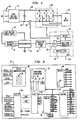
- FIG. 1 The diagram of Figure 1 shows the overall system for controlling a three phase asynchronous (induction) AC motor 10.
- a DC power source here depicted as a rectifier 12 coupled to a three phase AC line 14 provides DC voltage on positive and negative DC busses 16 and 18.
- the voltage on the busses 16 and 18 is typically several hundred volts.
- the busses are not referenced to ground and thus float with respect to ground.
- the negative bus is about 390 volts below ground.
- An inverter 20 of conventional structure comprises a plurality of transistor switches connected serially in pairs A-A′, B-B′ and C-C′ across the positive and negative busses and each switch pair junction point is connected to an input of the motor 10 to energize a phase of the motor.
- A′ means A-not and always has the opposite state of A.
- An exception is imposed by an anti-overlap function which may hold both switches open for an instant during a switching interval to insure that they are not both closed at any time.
- the trigger pulses for operating the transistor switches of inverter 20 are produced by a waveform generator 22 and coupled to the inverter 20 via an output circuit 24.
- the waveform generator 22, the output circuit 24, a serial communication (SC) circuit 26 and other support functions 28 described below are all part of a single ASIC chip 30 which is referenced to the potential of the negative bus 18.
- An isolating serial link 32 including two opto-isolators couples signals between the serial communication circuit 26 and microprocessor logic or microcontroller 34 which is referenced to ground potential and which generates signals to control the operation of the waveform generator 22.
- a conventional low voltage power supply 37 supports the microcontroller 34 and controls 36. Operator controls 36 provide inputs to the microcontroller 34.
- the grounded state of the logic allows control signals from external hardware such as switches, potentiometers, relays, programmable controllers, etc. to be directly connected to this portion of the circuitry without concern for operator or installer safety or the need for high voltage wiring.
- the microcontroller 34 and the operator controls afford an interface between the operator and the waveform generator 22 through the isolating link which protects both the operator and the microcontroller from the high voltages of the DC bus 18.
- the placement of the ASIC 30 in the high voltage side allows the three negative power switching devices A′, B′ and C′ to be directly driven (the positive switching devices being switched through simple level shifting circuitry), and allows high switching frequencies without the need for expensive opto-couplers or pulse transformers.
- Bus current can be sensed by a simple shunt resistor and voltage by resistive dividers, not shown. Positive bus voltage and each phase voltage is thus monitored. Average values of these analog signals are converted to digital form and sent through the serial port for control and readout purposes.
- the ASIC 30 generates other control signals in addition to the normal gating signals. It includes PWM signal generators to provide analog references, and also provides for an external analog to digital converter. It communicates with the microcontroller 34 through a serial port which can be optically coupled with low cost components.
- the ASIC is programmed by the microcontroller by means of several addressable eight bit registers. Status information from the ASIC may be read by the microcontroller in a similar manner.
- ASIC While several technology choices are available, it is here preferred to use CMOS gate array technology to form the ASIC.
- the ASIC is shown in Figure 2 and is divided into seven functional blocks. Each block has a set of registers associated with it by which the microcontroller establishes operating conditions or monitors the state of the ASIC or its inputs. For clarity, the signal busses interconnecting the blocks are not shown.
- the serial communications block 26 is responsible for transferring data between the ASIC 30 and the microcontroller 34. It operates in an asynchronous mode, and provides error checking. Address registers 38 in this block point to the other registers in the chip.
- the waveform generator 22 is the heart of the drive. It accepts 16 bit values in three registers 40, 42 and 44 for output frequency, carrier period, and duty cycle, respectively. It also includes a ROM 46 embodying lookup tables of reference voltage values and logic driven by the register contents for addressing the look up tables and for deriving pulse width modulated switching signals. The waveform generator produces three output phase signals based on a well defined algorithm which allows over-modulation, current limit, and both synchronous and asynchronous carrier types of operation. It calculates the period of the output frequency at sixty degree intervals.
- An output block 48 generates six gating signals from the three phase signals produced by the waveform generator 22. Its register 50 allows anti-overlap time to be programmed. It responds to an external current limit signal and to register bits which enable the output and allow phase interchange for reversing the motor. Three external fault signals and a current limit signal allow the fault block 52 to disable the drive and signal a fault to the microcontroller 34 through the serial port. A maximum current limit rate may be programmed. The fault block also monitors the gating signals and stores the number of the most recent gating signal to become active to allow diagnostic information to be displayed by the microcontroller.
- a control block 54 provides additional external inputs and outputs. It also contains registers which allow the microcontroller to manipulate bit signals in other blocks.
- Analog input and output is provided by two independent PWM signal generators and a parallel interface to an A/D converter in an analog block 56. This allows the microcontroller to monitor average bus current and to set current limit and dynamic braking references.
- a utility block 58 provides a crystal oscillator, a watchdog timer, test circuitry, and a timing signal generator.
- signals from the microcontroller are carried by the serial link 32 through an opto-isolator to the serial communications block which transfers the data to registers elsewhere on the chip according to addresses in the incoming signal.
- the data includes waveform information which is fed into the registers 40, 42 and 44 in the waveform generator 22. These registers are updated frequently by the microcontroller to continually control the waveform produced.
- the output of the waveform generator 22 is supplied to the output 48 which directly operates the negative inverter switches and operates the positive inverter switches through a simple level shifting circuit.
- An external current sensor 60 responsive to average bus current feeds a current signal to the analog circuit 56. Whenever the current exceeds a set limit, a limit signal is sent to the fault block 52, the control block 54 and the waveform generator. If this current limit occurs too often, the fault block issues a fault signal.
- the effect of the fault signal is to shut down the output circuit 48 to terminate inverter operation, and to set a fault flag in a status register in the control block 54.
- the fault block also latches into a register a code representing the type of fault which occurred and the last switch signal issued.
- the microcontroller regularly queries the status register and if a fault is found it also queries the fault block register to determine the cause of the fault.
- a watch dog circuit in the utility block 58 is reset each time the microcontroller queries the status register. If the query fails to occur within a preset time period indicative of microcontroller or serial link failure, the watch dog circuit signals the fault block which issues a fault signal to turn off the inverter.
- the ASIC chip provides a self sufficient control circuit able to function at the voltage level of the inverter bus and requiring only control data from the microcontroller which can readily be supplied over the serial link which is serviced by a relatively inexpensive optical coupler.
- the currents in the three phases of the motor required to establish the rotating field of the stator in one sector is determined by sequentially applying the two available voltages U1 and U2 on the DC bus to two phases and varying the time interval of each phase energization in a proportion to achieve the correct vector angle A at any instant ( Figure 4) and then progressively changing the angle with time to effect the field rotation.
- the voltage U1 is first applied by actuating switches A, B′ and C′ for a short interval and then actuating switches A, B and C′ to apply voltage U2 for another interval, the ratio of the two periods determining the effective vector angle of the field.
- a feature of the technique is that the pulses are applied in symmetrical groups to reduce harmonics. After an interval of no voltage, the voltage U2 is again applied followed by the voltage U1.
- the angle of the vector is correctly calculated by varying one of the energization intervals according to the function sin (A) and the other interval according to sin (60-A).
- the magnitude of the current is adjusted by using a variable duty cycle, that is, opening or closing all the positive switches so that no voltage is applied for a time.
- the interval of no voltage does not affect the angle, only the magnitude.
- pulse width modulation effects machine control where adjacent pulses actuate different switches for different intervals to create a rotating field vector and the pulse duty cycle determines the field strength or current in accordance with desired motor torque.
- the algorithm employs a carrier frequency (1kHz to 15kHZ) which is much greater than the machine frequency. It is assumed that the carrier is fixed for a particular application as a matter of design.
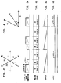
- Each carrier half period is normally divided into three states, as illustrated in Figure 5, the first two states being used to apply the two voltages U1 and U2 and the third state is used for the zero voltage (U3) interval.
- the periods of time spent in the first two states are determined by the values sin (A) and sin(60-A) which are stored in a look up table and which repeat at 60° intervals. These sine functions are compared to a free running counter whose rate of increment is inversely proportional to desired voltage amplitude.
- WAVEFORM GENERATOR Referring to Figure 6 the waveform algorithm is implemented in the ASIC chip. It is necessary for the microcontroller 34 to establish the desired motor operation by providing via the serial data link the machine frequency which is stored in the frequency register 40, the carrier period which is stored in the carrier register 44, and the duty cycle which is a quantity related to carrier period divided by duty cycle and is stored in the duty slope register 42. The look up table for the two sine functions is stored in ROM 46. With this information, the waveform generator is able to output the required switching commands.
- a stator angle calculator includes the frequency register 40, an adder 70, and an angle register 72 clocked at a fixed frequency.
- the angle register 72 is continuously incremented by the value of the frequency register 40.
- a portion of the angle register represents the ROM address of the angle A which is advanced to a latch 74 at the beginning of each carrier cycle as indicated in Figure 5(d).
- the appropriate sine value is loaded from the table into a shape register 76 via a data selector 78.
- Outputs 82 from a state machine 80 determine whether sin A or sin (60-A) is loaded into the shape register as well as the time of loading each value.
- a state machine output 84 also determines when a new angle may be latched into the ROM address.
- the carrier register 44 is coupled to a carrier counter 86 which is loaded with the register 44 value and counts down, reloads and counts down again to produce the ramps of Figure 5(c). When the counter 86 reaches zero it produces an output on line 88 which feeds into the state machine 80.
- the duty cycle generator is a variable slope ramp generator. It is constructed from the duty slope register 42, an adder 90 and a duty cycle register 92 which serves as an accumulator. The upper bits of the register are fed to a comparator 94 for comparison to a timing value.
- the duty cycle register 92 is clocked at a fixed rate via line 93 to add the slope register 42 contents to register 92 thereby creating a ramp shown by the broken lines in Figure 5(a).
- the ramp slope is thus determined by the contents of the duty slope register 42. As shown in Figure 5, when the ramp reaches the sine value the state changes and the ramp is reset to zero. This is accomplished by the comparator 94 which produces an output on line 96 to the state machine when the duty cycle register 92 count is greater than the shape register 76 value.
- the state machine in turn, produces a reset signal to the duty cycle register 92 on line 98.
- the reset signal can be used to hold the duty cycle register count at zero.
- Pulse Director A pulse director 100 determines from information on the present sector and a built-in table, which switches should be turned on for each vector and issues switch command signals on three output lines 102.
- the state machine 80 supplies the vector and timing information and a sector register 104 provides the sector information.
- the sector register 104 is a divide by six counter which is incremented by an overflow signal from the angle register 72 on line 105 whenever a 60° sector is completed.
- a current limit signal to the pulse director causes the pulse director 100 to gate the output signals to the same polarity to remove voltage from the motor.
- the pulse director also turns off a gate 101 to remove clock signals from the registers 72 and 92 and the counter 86 to freeze the action of the waveform generator as long as the current limit signal lasts.
- the overflow or sector complete signal on line 105 from the angle register 72 also provides inputs to a period register 106 and a counter 108 which is clocked at a constant rate. At the end of each sector the counter value is loaded into the register 106 and the counter 108 is reset.
- the period register holds a value which is a measure of the period and is used for feedback information to the microcontroller 34 to apprise the microcontroller of the period status in the event of an interruption by a current limit signal.
- the state machine 80 drives and coordinates the other components of the waveform generator. It is a logic circuit formed in the ASIC and is dedicated to the orderly operation of the generator.
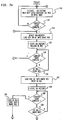
- the chart of Figure 7 illustrates the sequence of operation. Reference numerals in angle brackets ⁇ nn> refer to the numerals of blocks functions being described. In conjunction with Figure 5, the timing and interaction of the several register outputs is readily under stood. Assuming that the machine enters state 0 at power up, the duty cycle register is held in reset mode ⁇ 110>. When the carrier count is complete ⁇ 112>, the row pointer is updated (via line 84), and sin(60-A) is loaded into the shape register 76 ⁇ 114>.
- This process is the regular progression of the state machine which sequences through all six states as shown in Figure 5 and applies up to 100% modulation. At that point the 3 state and the 0 state are reduced to zero time period and, at over-modulation, the 2 state is truncated by the carrier count completion prior to the duty cycle register count reaching the shape register value as shown in Figure 8. To assure that the 2 state and the 4 state have equal periods to maintain symmetry, the value of the duty cycle register is loaded into the shape register as indicated at Figure 8(a). This is accomplished by the data selector 78 which is triggered by the state machine to load data from the duty cycle register 92 instead of from the table 46. Then during the 4 state the duty cycle register will reach the shape register value at the correct time.
- the state machine toggles between 1 state and 5 state to produce a square wave input to the motor.
- the state machine goes to block 142 to load the shape register and then to block 144 to enter 5 state. Then if the carrier count is completed ⁇ 146> the logic flows to block 114 to prepare for the 1 state.
- the operation of the waveform generator is usually asynchronous but it is sometimes desirable, particularly at high stator frequency, to operate synchronously wherein the carrier frequency is an integral multiple of stator frequency.
- a switch 160 under control of the microcontroller 34 can be closed to command synchronous operation.
- the switch connects the sector completion signal on line 105 to the carrier counter 86 to force a reset of the counter and to issue a carrier count complete signal.
- the microcontroller 34 sets stator frequency and carrier period values which approximate synchronous conditions so that at the end of a 60° sector the carrier count is close to zero as shown in Figure 9.
- the sector completion signal is issued on line 105 any error in the carrier count is removed by resetting the carrier count to zero and the state machine to 1 state via the carrier count completion signal and the new 60° sector is begun.
- an approximately even number of carrier half cycles occur between the sector completion signals on line 105 shown in part (b) of Figure 9. The last half cycle is truncated at the end of the sector.
- the waveform generator is able to produce a PWM output for controlling the inverter switches in a manner to produce a rotating field having a frequency dependent on the contents of the frequency register and a magnitude dependent on the contents of the duty slope register.
- the switching pulses are produced at a rate determined by the contents of the carrier register. Generally four pulses per period are produced unless a square wave is produced at two pulses per period.
- the waveform generator can smoothly change into and out of an over-modulation condition and can switch between synchronous and asynchronous operation.
- the microcontroller is in control of the waveform generator at all times except when a current limit is detected or a fault is detected in which case the generator function is frozen for a time or stopped altogether.
- the register contents can be updated at any time by the microcontroller.
Landscapes
- Engineering & Computer Science (AREA)
- Power Engineering (AREA)
- Control Of Ac Motors In General (AREA)
- Inverter Devices (AREA)
Applications Claiming Priority (2)
| Application Number | Priority Date | Filing Date | Title |
|---|---|---|---|
| US07/560,112 US4994950A (en) | 1990-07-31 | 1990-07-31 | Waveform generator for inverter control |
| US560112 | 1990-07-31 |
Publications (3)
| Publication Number | Publication Date |
|---|---|
| EP0469873A2 true EP0469873A2 (de) | 1992-02-05 |
| EP0469873A3 EP0469873A3 (en) | 1992-05-20 |
| EP0469873B1 EP0469873B1 (de) | 1995-09-13 |
Family
ID=24236425
Family Applications (1)
| Application Number | Title | Priority Date | Filing Date |
|---|---|---|---|
| EP91306998A Expired - Lifetime EP0469873B1 (de) | 1990-07-31 | 1991-07-30 | Wellenformgenerator für Wechselrichtersteuerung |
Country Status (4)
| Country | Link |
|---|---|
| US (1) | US4994950A (de) |
| EP (1) | EP0469873B1 (de) |
| CA (1) | CA2047322C (de) |
| DE (1) | DE69112957T2 (de) |
Cited By (5)
| Publication number | Priority date | Publication date | Assignee | Title |
|---|---|---|---|---|
| WO1997044887A1 (de) * | 1996-05-21 | 1997-11-27 | Siemens Aktiengesellschaft | Umrichtersystem |
| WO2003073185A3 (en) * | 2002-02-28 | 2004-02-05 | Zetacon Corp | Predictive control system and method |
| EP1363389A3 (de) * | 2002-05-17 | 2006-02-22 | Vacon Oyj | Wechselrichtersteuerung |
| RU2320071C1 (ru) * | 2006-10-09 | 2008-03-20 | Государственное образовательное учреждение высшего профессионального образования "Южно-Уральский государственный университет" | Фазосдвигающее устройство |
| WO2017184846A1 (en) * | 2016-04-21 | 2017-10-26 | The Florida State University Research Foundation, Inc. | A self-balanced modulation and magnetic rebalancing method for parallel multilevel inverters |
Families Citing this family (38)
| Publication number | Priority date | Publication date | Assignee | Title |
|---|---|---|---|---|
| JP2812528B2 (ja) * | 1990-03-20 | 1998-10-22 | 株式会社日立製作所 | インバータ回路 |
| DE69113528T2 (de) * | 1990-07-06 | 1996-02-29 | Hitachi Ltd | Bürstenloser Motor mit eingebautem integriertem Schaltkreis, welcher einen peripheren Schaltkreis mit einem Chip beinhaltet. |
| DE69127664T2 (de) * | 1990-07-20 | 1998-02-12 | Toshiba Kawasaki Kk | Vorrichtung zur Erzeugung eines dreiphasigen PWM-Signals für Wechselrichter |
| JP2950939B2 (ja) * | 1990-08-02 | 1999-09-20 | 株式会社日立製作所 | インバータ装置 |
| JP3156269B2 (ja) * | 1991-04-10 | 2001-04-16 | 松下電器産業株式会社 | ディジタル三相pwm波形発生装置 |
| KR950004836B1 (ko) * | 1991-10-21 | 1995-05-13 | 삼성전자 주식회사 | 교류 전동기의 상전압 측정장치 및 그 측정방법 |
| US5499177A (en) * | 1992-04-22 | 1996-03-12 | Fuji Electric Co., Ltd. | Inverter device with a circuit for generating pulse width modulation signals |
| US5400237A (en) * | 1992-05-11 | 1995-03-21 | Simmonds Precision Products, Inc. | PWM inverter controller with waveform memory |
| US5298851A (en) * | 1992-05-12 | 1994-03-29 | Transpo Electronics, Inc. | Multiple application voltage regulator system and method |
| US5461296A (en) * | 1993-07-20 | 1995-10-24 | Eaton Corporation | Bumpless rotating start |
| US5486747A (en) * | 1993-07-29 | 1996-01-23 | United Technologies Motor Systems | General purpose motor controller |
| US5386186A (en) * | 1993-08-04 | 1995-01-31 | Eaton Corporation | Stator flux oriented control |
| US5537308A (en) * | 1993-10-15 | 1996-07-16 | Eaton Corporation | Digital current regulator |
| US5625545A (en) * | 1994-03-01 | 1997-04-29 | Halmar Robicon Group | Medium voltage PWM drive and method |
| US5672950A (en) * | 1994-08-16 | 1997-09-30 | Itt Corporation | Voltage, phase and frequency control by miniature inverter system |
| US5581169A (en) * | 1994-08-31 | 1996-12-03 | Allen-Bradley Company, Inc. | Apparatus used with an inverter/converter eliminating unintended voltage pulses |
| FR2746982B1 (fr) * | 1996-03-28 | 1998-05-07 | Schneider Electric Sa | Convertisseur de frequence pour moteur alternatif |
| US5793174A (en) * | 1996-09-06 | 1998-08-11 | Hunter Douglas Inc. | Electrically powered window covering assembly |
| DE19648696A1 (de) * | 1996-11-25 | 1998-05-28 | Asea Brown Boveri | Verfahren und Vorrichtung zur Ausregelung des DC-Offsets eines Umrichters |
| US6069808A (en) * | 1997-05-21 | 2000-05-30 | Texas Instruments Incorporated | Symmetrical space vector PWM DC-AC converter controller |
| US6215261B1 (en) * | 1999-05-21 | 2001-04-10 | General Electric Company | Application specific integrated circuit for controlling power devices for commutating a motor based on the back emf of motor |
| JP4131079B2 (ja) * | 2000-07-12 | 2008-08-13 | 株式会社安川電機 | インバータ装置およびその電流制限方法 |
| GB0213098D0 (en) * | 2002-06-07 | 2002-07-17 | Trw Ltd | Motor control device |
| TWI256759B (en) * | 2004-04-16 | 2006-06-11 | Yu-Lin Chi | Digitalized power control system |
| JP2006101471A (ja) * | 2004-09-06 | 2006-04-13 | Hitachi Communication Technologies Ltd | マルチキャスト冗長経路ルータ、マルチキャスト冗長化方式 |
| US20060268975A1 (en) * | 2005-05-13 | 2006-11-30 | Bors Douglas A | Pulse width modulation (PWM) utilizing a randomly generated pattern subsequently modified to create desired control characteristics |
| US7535185B2 (en) * | 2005-10-26 | 2009-05-19 | Itt Manufacturing Enterprises, Inc. | Method and system for implementing power reduction algorithms in a night vision system power system |
| JP2008236983A (ja) * | 2007-03-23 | 2008-10-02 | Matsushita Electric Ind Co Ltd | モータ駆動装置およびモータ駆動方法 |
| JP2008312342A (ja) * | 2007-06-14 | 2008-12-25 | Sanden Corp | 電動圧縮機の制御装置 |
| JP2009033919A (ja) * | 2007-07-30 | 2009-02-12 | Nec Electronics Corp | 誘導モータの制御装置及び誘導モータの制御方法 |
| GB0908111D0 (en) * | 2009-05-12 | 2009-06-24 | Peto Raymond J | A motor controller & related method |
| JP5372705B2 (ja) | 2009-11-04 | 2013-12-18 | 株式会社日立産機システム | 電力変換装置 |
| US9030851B2 (en) * | 2010-04-30 | 2015-05-12 | Rockwell Automation Technologies, Inc. | DC bus voltage control method and system |
| JP5569465B2 (ja) * | 2010-05-28 | 2014-08-13 | 株式会社デンソー | 振幅変調装置の異常診断装置 |
| JP5939236B2 (ja) * | 2013-11-29 | 2016-06-22 | 株式会社デンソー | モータ制御装置 |
| JP6131906B2 (ja) * | 2014-04-08 | 2017-05-24 | 富士電機株式会社 | リンプホームシステム、その安全制御装置 |
| CN112994579B (zh) * | 2021-03-10 | 2023-10-10 | 苏州汇川联合动力系统股份有限公司 | 逆变器驱动信号调制方法、设备及计算机可读存储介质 |
| ES2994963B2 (es) * | 2023-07-28 | 2025-08-01 | Desarrollos Ind Ecodein S L | Sistema para controlar y optimizar el consumo electrico aplicado a una resistencia electrica |
Family Cites Families (9)
| Publication number | Priority date | Publication date | Assignee | Title |
|---|---|---|---|---|
| US4656572A (en) * | 1985-02-19 | 1987-04-07 | Westinghouse Electric Corp. | PWM inverter |
| JPH0636676B2 (ja) * | 1985-03-01 | 1994-05-11 | 勲 高橋 | Pwmインバ−タの制御方法 |
| JPS62118774A (ja) * | 1985-11-18 | 1987-05-30 | Toshiba Corp | インバ−タのパルス幅変調信号発生方式 |
| JPH0697854B2 (ja) * | 1986-01-11 | 1994-11-30 | 株式会社日立製作所 | 電力変換装置の制御装置 |
| JPH0669305B2 (ja) * | 1986-03-05 | 1994-08-31 | サンケン電気株式会社 | インバータによるモータ制御装置 |
| JPH0834694B2 (ja) * | 1986-10-25 | 1996-03-29 | 株式会社日立製作所 | 電力変換器の制御装置 |
| JPH0681513B2 (ja) * | 1987-11-12 | 1994-10-12 | 株式会社東芝 | Pwm制御装置 |
| JPH0793823B2 (ja) * | 1988-02-01 | 1995-10-09 | 株式会社日立製作所 | 電圧形インバータのpwm制御装置 |
| JP2821679B2 (ja) * | 1988-07-19 | 1998-11-05 | 株式会社日立製作所 | Pwmインバータのゲート信号発生方法および装置、pwmインバータ装置 |
-
1990
- 1990-07-31 US US07/560,112 patent/US4994950A/en not_active Expired - Fee Related
-
1991
- 1991-07-18 CA CA002047322A patent/CA2047322C/en not_active Expired - Fee Related
- 1991-07-30 EP EP91306998A patent/EP0469873B1/de not_active Expired - Lifetime
- 1991-07-30 DE DE69112957T patent/DE69112957T2/de not_active Expired - Fee Related
Cited By (9)
| Publication number | Priority date | Publication date | Assignee | Title |
|---|---|---|---|---|
| WO1997044887A1 (de) * | 1996-05-21 | 1997-11-27 | Siemens Aktiengesellschaft | Umrichtersystem |
| US6021057A (en) * | 1996-05-21 | 2000-02-01 | Siemens Aktiengesellschaft | Inverter system |
| WO2003073185A3 (en) * | 2002-02-28 | 2004-02-05 | Zetacon Corp | Predictive control system and method |
| US7243006B2 (en) | 2002-02-28 | 2007-07-10 | Zetacon Corporation | Predictive control system and method |
| US7286906B2 (en) | 2002-02-28 | 2007-10-23 | Zetacon Corporation | Predictive control system and method |
| EP1363389A3 (de) * | 2002-05-17 | 2006-02-22 | Vacon Oyj | Wechselrichtersteuerung |
| RU2320071C1 (ru) * | 2006-10-09 | 2008-03-20 | Государственное образовательное учреждение высшего профессионального образования "Южно-Уральский государственный университет" | Фазосдвигающее устройство |
| WO2017184846A1 (en) * | 2016-04-21 | 2017-10-26 | The Florida State University Research Foundation, Inc. | A self-balanced modulation and magnetic rebalancing method for parallel multilevel inverters |
| US9831800B2 (en) | 2016-04-21 | 2017-11-28 | The Florida State University Research Foundation, Inc. | Self-balanced modulation and magnetic rebalancing method for parallel multilevel inverters |
Also Published As
| Publication number | Publication date |
|---|---|
| US4994950A (en) | 1991-02-19 |
| CA2047322A1 (en) | 1992-02-01 |
| CA2047322C (en) | 1998-04-28 |
| EP0469873B1 (de) | 1995-09-13 |
| DE69112957T2 (de) | 1996-05-15 |
| DE69112957D1 (de) | 1995-10-19 |
| EP0469873A3 (en) | 1992-05-20 |
Similar Documents
| Publication | Publication Date | Title |
|---|---|---|
| US4994950A (en) | Waveform generator for inverter control | |
| US5045988A (en) | Isolated adjustable frequency AC inverter control | |
| US4290108A (en) | Control unit for a converter | |
| US3694718A (en) | Methods of inverter voltage control by superimposed chopping | |
| US5034675A (en) | Polyphase machine fed by a pulse-controlled a.c. converter | |
| US4870556A (en) | Method and apparatus for controlling power converter | |
| CA2112238A1 (en) | Programmed pwm inverter controller | |
| KR920004905B1 (ko) | Pwm 제어장치 | |
| CA1292770C (en) | Apparatus and method for controlling a force commutated inverter | |
| US5264775A (en) | Pulse width modulation control apparatus and method | |
| US4466070A (en) | Control unit with digital addressing memory for a DC-to-AC inverter | |
| US11342878B1 (en) | Regenerative medium voltage drive (Cascaded H Bridge) with reduced number of sensors | |
| US5528486A (en) | Firing pattern output generation for AC traction inverter control | |
| CA2147186C (en) | Unity trapezoidal wave rms regulator | |
| US4914371A (en) | Apparatus for controlling AC servo motor | |
| US4267570A (en) | Control unit for multi-phase static converter | |
| US4729087A (en) | Inversion process and apparatus | |
| GB2051507A (en) | Selective commutation circuit for an inverter | |
| JP2527880Y2 (ja) | 点弧制御回路 | |
| EP0083866A2 (de) | Leistungsumformer für Wechselstrom | |
| US4685049A (en) | Unrestricted frequency changer switch topology | |
| GB2125239A (en) | A three phase supply synthesis arrangement | |
| JP2710792B2 (ja) | デイジタル移相器 | |
| Brickwedde et al. | Microprocessor controlled 50KVA PWM inverter motor drive | |
| US5387856A (en) | Speed control arrangements for electric motors |
Legal Events
| Date | Code | Title | Description |
|---|---|---|---|
| PUAI | Public reference made under article 153(3) epc to a published international application that has entered the european phase |
Free format text: ORIGINAL CODE: 0009012 |
|
| AK | Designated contracting states |
Kind code of ref document: A2 Designated state(s): DE GB IT |
|
| PUAL | Search report despatched |
Free format text: ORIGINAL CODE: 0009013 |
|
| AK | Designated contracting states |
Kind code of ref document: A3 Designated state(s): DE GB IT |
|
| 17P | Request for examination filed |
Effective date: 19920630 |
|
| 17Q | First examination report despatched |
Effective date: 19940422 |
|
| GRAA | (expected) grant |
Free format text: ORIGINAL CODE: 0009210 |
|
| AK | Designated contracting states |
Kind code of ref document: B1 Designated state(s): DE GB IT |
|
| REF | Corresponds to: |
Ref document number: 69112957 Country of ref document: DE Date of ref document: 19951019 |
|
| ITF | It: translation for a ep patent filed | ||
| PLBE | No opposition filed within time limit |
Free format text: ORIGINAL CODE: 0009261 |
|
| STAA | Information on the status of an ep patent application or granted ep patent |
Free format text: STATUS: NO OPPOSITION FILED WITHIN TIME LIMIT |
|
| 26N | No opposition filed | ||
| REG | Reference to a national code |
Ref country code: GB Ref legal event code: IF02 |
|
| PGFP | Annual fee paid to national office [announced via postgrant information from national office to epo] |
Ref country code: GB Payment date: 20030612 Year of fee payment: 13 |
|
| PGFP | Annual fee paid to national office [announced via postgrant information from national office to epo] |
Ref country code: DE Payment date: 20030731 Year of fee payment: 13 |
|
| PG25 | Lapsed in a contracting state [announced via postgrant information from national office to epo] |
Ref country code: GB Free format text: LAPSE BECAUSE OF NON-PAYMENT OF DUE FEES Effective date: 20040730 |
|
| PG25 | Lapsed in a contracting state [announced via postgrant information from national office to epo] |
Ref country code: DE Free format text: LAPSE BECAUSE OF NON-PAYMENT OF DUE FEES Effective date: 20050201 |
|
| GBPC | Gb: european patent ceased through non-payment of renewal fee |
Effective date: 20040730 |
|
| PG25 | Lapsed in a contracting state [announced via postgrant information from national office to epo] |
Ref country code: IT Free format text: LAPSE BECAUSE OF NON-PAYMENT OF DUE FEES;WARNING: LAPSES OF ITALIAN PATENTS WITH EFFECTIVE DATE BEFORE 2007 MAY HAVE OCCURRED AT ANY TIME BEFORE 2007. THE CORRECT EFFECTIVE DATE MAY BE DIFFERENT FROM THE ONE RECORDED. Effective date: 20050730 |