EP0465167B1 - Schwellenfreie logische Schaltung - Google Patents
Schwellenfreie logische Schaltung Download PDFInfo
- Publication number
- EP0465167B1 EP0465167B1 EP91305895A EP91305895A EP0465167B1 EP 0465167 B1 EP0465167 B1 EP 0465167B1 EP 91305895 A EP91305895 A EP 91305895A EP 91305895 A EP91305895 A EP 91305895A EP 0465167 B1 EP0465167 B1 EP 0465167B1
- Authority
- EP
- European Patent Office
- Prior art keywords
- transistor
- base
- emitter
- mntl
- collector
- Prior art date
- Legal status (The legal status is an assumption and is not a legal conclusion. Google has not performed a legal analysis and makes no representation as to the accuracy of the status listed.)
- Expired - Lifetime
Links
Images


Classifications
-
- H—ELECTRICITY
- H03—ELECTRONIC CIRCUITRY
- H03K—PULSE TECHNIQUE
- H03K19/00—Logic circuits, i.e. having at least two inputs acting on one output; Inverting circuits
- H03K19/02—Logic circuits, i.e. having at least two inputs acting on one output; Inverting circuits using specified components
- H03K19/08—Logic circuits, i.e. having at least two inputs acting on one output; Inverting circuits using specified components using semiconductor devices
- H03K19/082—Logic circuits, i.e. having at least two inputs acting on one output; Inverting circuits using specified components using semiconductor devices using bipolar transistors
- H03K19/086—Emitter coupled logic
-
- H—ELECTRICITY
- H03—ELECTRONIC CIRCUITRY
- H03K—PULSE TECHNIQUE
- H03K19/00—Logic circuits, i.e. having at least two inputs acting on one output; Inverting circuits
- H03K19/01—Modifications for accelerating switching
- H03K19/013—Modifications for accelerating switching in bipolar transistor circuits
- H03K19/0136—Modifications for accelerating switching in bipolar transistor circuits by means of a pull-up or down element
Definitions
- This invention relates to a modified non-threshold logic (MNTL) circuit, and more particularly to, an MNTL circuit including a monolithic basic gate circuit and an emitter follower circuit which drives a wiring load capacitor.
- MNTL non-threshold logic
- a conventional MNTL circuit includes an MNTL, basic gate circuit and an emitter follower circuit.
- a driving transistor which is driven by the MNTL basic gate circuit supplies an output level to an output terminal thereof.
- an output signal of the emitter follower circuit becomes high level to charge up a wiring stray capacitance existing between the output terminal and a lower power supply level.
- the driving transistor becomes OFF state, charges accumulated in the wiring stray capacitance are discharged toward the lower supply level through a resistor, and the output signal of the emitter follower circuit becomes low level.
- a propagation delay time of the output signal thereof is relatively long, because a fall time of the output signal is long as compared with a building-up (rise) time thereof.
- the fall time of the output signal is dependent on a discharging time of the charges accumulated in the wiring stray capacitance through the resistor.
- an object of the invention to provide an MNTL circuit in which a propagation delay time of an output signal thereof is shortened.
- a modified non-threshold logic circuit comprises: an MNTL basic gate circuit connected between a first and second power supply line and comprising first, second and third transistors, one of said first and second transistors taking an ON state when the other takes an OFF state, said first transistor being connected to an input terminal and controlled by an input voltage applied to a base of said first transistor, said second transistor being connected to a reference terminal and controlled by a reference voltage applied to a base of said second transistor, and said third transistor being connected to a constant current supply terminal and controlled by a constant current supply voltage applied to a base of said third transistor to pass a constant current through said third transistor, an emitter resistor interconnected between an emitter of said first transistor and a collector of said third transistor, a speed up capacitor connected in parallel to said emitter resistor between said emitter of said first transistor and said collector of said third transistor, and characterised by an emitter follower circuit comprising a driving transistor having a base connected to a collector of said first transistor and a collector connected to the first power supply line
- the conventional MNTL circuit includes an MNTL basic gate circuit 10 and an emitter follower circuit 30.
- the MNTL basic gate circuit 10 includes first to third NPN transistors 13, 14 and 19, first and second collector resistors 15 and 16, an emitter resistor 17 and a resistor 21, and a capacitor 18.
- the first NPN transistor 13 is connected at a base to an input terminal 11 to which an input voltage V IN is applied, at a collector to a nodal point A, and at an emitter to a nodal point C.
- the second NPN transistor 14 is connected at a base to a reference terminal 12 to which a reference voltage V REF is applied, at a collector to a nodal point B, and at an emitter to a nodal point D.
- the third NPN transistor 19 is connected at a base to a current supply terminal 20 to which a constant current supply voltage V CSI is applied by which a constant current flows through the third NPN transistor 19, at a collector to the nodal point D, and at an emitter to a nodal point E.
- the first collector resistor 15 is connected at a first terminal to a first power supply line 1 from which a first power supply voltage V cc (which is normally a ground level GND) is applied, and at a second terminal to the nodal point A.
- the second collector resistor 16 is connected at a first terminal to the first power supply line 1 and at a second terminal to the nodal point B.
- the emitter resistor 17 is connected at a first terminal to the nodal point C and at a second terminal to the nodal point D.
- the resistor 21 is connected at a first terminal to the nodal point E and at a second terminal to a second power supply line 2 from which a second power supply voltage V EE (which is normally a level lower than the ground level GND) is applied.
- the speed up capacitor 18 is connected at a first terminal to the nodal point C and at a second terminal to the nodal point D.
- the emitter follower circuit 30 includes a driving transistor 31, a resistor 32.
- the driving transistor 31 is connected at a base to the nodal point A of the MNTL basic gate circuit 10, at a collector to the first power supply line 1, and at an emitter to a nodal point F which is connected to an output terminal 34.
- the resistor 32 is connected at a first terminal to the nodal point F and at a second terminal to the second power supply line 2. There exists a wiring stray capacitance 33 between output terminal 34 and the second power supply line 2.
- the wiring stray capacitance 33 is shown to be positioned between the output terminal 34 and the second power supply line 2, because a potential of an IC substrate for incorporating the MNTL circuit is equal to that of the second power supply line 2, so that the wiring stray capacitance 33 is more dominant than a stray capacitance generated between the output terminal 34 and the first power supply line 1.
- the first and second transistors 13 and 14 become ON state selectively in an alternative way.
- the input voltage V IN of a low level is applied to the base of the first transistor 13 through the input terminal 11 to make the first transistor 13 OFF state, no current flows through the first collector resistor 15 and no voltage drop occurs, so that the nodal point A becomes the same level as the first power supply line 1 having a high level V cc .
- the base of the driving transistor 31 of the emitter follower circuit 30 is applied with the high level V cc to make the driving transistor 31 ON state, so that an output level of the emitter of the driving transistor 31 as an output signal of the emitter follower circuit 30 becomes high level and the wiring stray capacitance 33 is charged up.
- the MNTL circuit includes an MNTL basic gate circuit 10 and an emitter follower circuit 40.
- the MNTL basic gate circuit 10 has the same circuitry structure as shown in Fig. 1, so that the description thereof will be omitted.
- First and second power supply lines 1 and 2 are also the same as those in Fig. 1.
- the emitter follower circuit 40 includes driving, clamping and pull down transistors 41, 42 and 43, a resistor 47, and a coupling capacitor 46.
- the driving transistor 41 is connected at a base to a nodal point A of the MNTL basic gate circuit 10, at a collector to the first power supply line 1, and at an emitter to a nodal point F which is connected to an output terminal 48.
- the clamping transistor 42 is connected at a base to a clamp terminal 45 to which a clamp voltage V CLP is applied, at a collector to the first power supply line 1, and at an emitter to a nodal point G.
- the pull down transistor 43 which composes a push pull circuitry structure is connected at a base to the nodal point G, at a collector to the nodal point F, and at an emitter to the second power supply line 2.
- the bias resistor 47 which has a high resistance is connected at a first terminal to the nodal point G and at a second terminal to the second power supply line 2.
- the coupling capacitor 46 is connected at a first terminal to the nodal point G and at a second terminal to an input terminal 11 of the MNTL basic gate circuit 10.
- a voltage V BE between the base and emitter of the pull down transistor 43 is biased regularly by the clamping transistor 42 and the bias resistor 47 to improve an impulse response thereof.
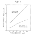
- Fig. 3 is a graph showing a relation between a propagation delay time t pd and a wiring stray capacitance C L of the MNTL circuit according to the present invention as well as the conventional MNTL circuit calculated by simulation.
- the propagation delay time t pd is shortened by 64.2%, 55.4% and 56.7% as compared with those in the conventional MNTL circuit when the wiring stray capacitance C L is approximately 0.1 pF, 0.3 pF, 0.6 pF, respectively.
Landscapes
- Engineering & Computer Science (AREA)
- Physics & Mathematics (AREA)
- Computer Hardware Design (AREA)
- Computing Systems (AREA)
- General Engineering & Computer Science (AREA)
- Mathematical Physics (AREA)
- Power Engineering (AREA)
- Logic Circuits (AREA)
Claims (2)
- Modifizierte schwellenwertfreie Logik-Schaltung (MNTL; modified non-threshold logic), die aufweist:
eine MNTL-Grundgatterschaltung (10), die zwischen einer ersten (1) und einer zweiten (2) Leistungsversorgungsleitung verbunden ist und erste (13), zweite (14) und dritte (19) Transistoren aufweist, wobei einer der ersten und zweiten Transistoren den EIN-Zustand einnimmt, wenn der andere den AUS-Zustand einnimmt, wobei der erste Transistor mit einem Eingangsanschluß (11) verbunden ist und durch eine Eingangsspannung VIN gesteuert wird, die an die Basis des ersten Transistors angelegt wird, wobei der zweite Transistor mit einem Bezugsanschluß (12) verbunden ist und durch eine Bezugsspannung gesteuert wird, die an die Basis des zweiten Transistors angelegt wird, und wobei der dritte Transistor mit einem Konstantstromversorgungsanschluß (20) verbunden ist und durch eine Konstantstromversorgungsspannung gesteuert wird, die an die Basis des dritten Transistors angelegt wird, um einen konstanten Strom durch den dritten Transistor hindurchzuleiten, einen Emitter-Widerstand (17), der zwischen dem Ermitter des ersten Transistors (13) und dem Kollektor des dritten Transistors (19) verbunden ist, einen Beschleunigungskondensator (18), der parallel mit dem Ermitter-Widerstand (17) zwischen dem Ermitter des ersten Transistors und dem Kollektor des dritten Transistors verbunden ist, und die gekennzeichnet ist durch eine Ermitterfolgerschaltung (40), die einen Treibertransistor (41), der mit der Basis mit dem Kollektor des ersten Transistors (13) und der mit dem Kollektor mit der ersten Leistungsversorgungsleitung (1) verbunden ist, einen Pull-Down-Transistor (43), der mit seinem Kollektor mit dem Ermitter des Treibertransistors (41) verbunden ist, einen Klemm-, Bregrenzungs- oder Abfangtransistor (clamping transistor 42), der mit dem Ermitter mit der Basis des Pull-Down-Transistors (43) verbunden ist, einen Vorspannungswiderstand (47), der an seinem einen Ende mit der Basis des Pull-Down-Transistors (43) und mit dem anderen Ende mit der zweiten Leistungsversorgungsleitung (2) verbunden ist, und einen Kopplungskondensator (46) aufweist, der zwischen dem einen Ende des Vorspannungswiderstandes (47) und der Basis des ersten Transistors (13) verbunden ist, wobei der Treibertransistor (41) durch ein Kollektorausgangssignal vom ersten Transistor (13) der MNTL-Grundgatterschaltung (10) gesteuert wird, das an die Basis des Treibertransistors angelegt wird, wobei der Pull-Down-Transistor (43) an seiner Basis durch den Klemm-, Bregrenzungs- oder Abfangtransistor (42) vorgespannt wird, wobei der Vorspannungswiderstand (47) einen hohen Widerstandswert hat. - MNTL-Schaltung nach Anspruch 1, bei der der Pull-Down-Transistor an seiner Basis mit einem Punkt verbunden ist, der mit einem Eingangsspannungsanschluß verbunden ist.
Applications Claiming Priority (2)
| Application Number | Priority Date | Filing Date | Title |
|---|---|---|---|
| JP2173945A JP2861300B2 (ja) | 1990-06-29 | 1990-06-29 | Mntl型半導体集積回路装置 |
| JP173945/90 | 1990-06-29 |
Publications (3)
| Publication Number | Publication Date |
|---|---|
| EP0465167A2 EP0465167A2 (de) | 1992-01-08 |
| EP0465167A3 EP0465167A3 (en) | 1992-04-01 |
| EP0465167B1 true EP0465167B1 (de) | 1996-09-18 |
Family
ID=15969981
Family Applications (1)
| Application Number | Title | Priority Date | Filing Date |
|---|---|---|---|
| EP91305895A Expired - Lifetime EP0465167B1 (de) | 1990-06-29 | 1991-06-28 | Schwellenfreie logische Schaltung |
Country Status (4)
| Country | Link |
|---|---|
| US (1) | US5187391A (de) |
| EP (1) | EP0465167B1 (de) |
| JP (1) | JP2861300B2 (de) |
| DE (1) | DE69122184T2 (de) |
Families Citing this family (3)
| Publication number | Priority date | Publication date | Assignee | Title |
|---|---|---|---|---|
| JPH04334121A (ja) * | 1991-05-09 | 1992-11-20 | Nec Corp | 能動プルダウン回路 |
| DE4321482C1 (de) * | 1993-06-28 | 1994-12-08 | Siemens Ag | Digitale Schaltstufe mit Stromschalter |
| JP2679644B2 (ja) * | 1994-10-03 | 1997-11-19 | 日本電気株式会社 | Ntl論理回路用電源回路 |
Family Cites Families (7)
| Publication number | Priority date | Publication date | Assignee | Title |
|---|---|---|---|---|
| US4626709A (en) * | 1984-09-28 | 1986-12-02 | Advanced Micro Devices, Inc. | Dynamic push-pull for ECL |
| US4695749A (en) * | 1986-02-25 | 1987-09-22 | Fairchild Semiconductor Corporation | Emitter-coupled logic multiplexer |
| US4687953A (en) * | 1986-04-18 | 1987-08-18 | Advanced Micro Devices, Inc. | Dynamic ECL line driver circuit |
| US5073728A (en) * | 1987-07-15 | 1991-12-17 | Texas Instruments Incorporated | Active load for ECL type outputs |
| US5027013A (en) * | 1987-11-17 | 1991-06-25 | Applied Micro Circuits Corporation | Method and apparatus for coupling an ECL output signal using a clamped capacitive bootstrap circuit |
| US4835420A (en) * | 1987-11-17 | 1989-05-30 | Applied Micro Circuits Corporation | Method and apparatus for signal level conversion with clamped capacitive bootstrap |
| US4948991A (en) * | 1988-11-03 | 1990-08-14 | Motorola Inc. | Load controlled ECL transient driver |
-
1990
- 1990-06-29 JP JP2173945A patent/JP2861300B2/ja not_active Expired - Lifetime
-
1991
- 1991-06-28 EP EP91305895A patent/EP0465167B1/de not_active Expired - Lifetime
- 1991-06-28 DE DE69122184T patent/DE69122184T2/de not_active Expired - Fee Related
- 1991-07-01 US US07/723,921 patent/US5187391A/en not_active Expired - Fee Related
Non-Patent Citations (1)
| Title |
|---|
| PATENT ABSTRACTS OF JAPAN, VOL. 14, NO. 348 (E-957) (4291), 27th JULY 1990; & JP-A-2 121 409 * |
Also Published As
| Publication number | Publication date |
|---|---|
| EP0465167A2 (de) | 1992-01-08 |
| JPH0463018A (ja) | 1992-02-28 |
| EP0465167A3 (en) | 1992-04-01 |
| DE69122184T2 (de) | 1997-01-30 |
| JP2861300B2 (ja) | 1999-02-24 |
| DE69122184D1 (de) | 1996-10-24 |
| US5187391A (en) | 1993-02-16 |
Similar Documents
| Publication | Publication Date | Title |
|---|---|---|
| US4779014A (en) | BiCMOS logic circuit with additional drive to the pull-down bipolar output transistor | |
| US6236248B1 (en) | Output buffer circuit | |
| EP0329285B1 (de) | Ausgangspuffer | |
| EP0530159B1 (de) | Einschaltrücksetzschaltung ohne Stromverbrauch | |
| GB1601999A (en) | Protection circuit for transistorised switch | |
| EP0225431B1 (de) | Gepufferte Schaltung zur Kompensierung des Millerstromes | |
| WO2021124644A1 (ja) | ゲート駆動回路 | |
| US4437021A (en) | Line driver circuit | |
| US4880998A (en) | Bipolar transistor and CMOS transistor logic circuit having improved discharge capabilities | |
| USRE37778E1 (en) | Current limiting circuit | |
| US5786709A (en) | Integrated circuit output driver incorporating power distribution noise suppression circuitry | |
| US6147542A (en) | Galvanic isolation for inputs with a pull-up | |
| EP0465167B1 (de) | Schwellenfreie logische Schaltung | |
| KR19990008121A (ko) | Gtl 출력 증폭기 | |
| EP0046498A1 (de) | Bootstrap-Treiberschaltung | |
| JP2561003B2 (ja) | アクティブプルダウン型ecl回路 | |
| US5896058A (en) | High speed totem pole FET driver circuit with differential cross conduction prevention | |
| KR100194298B1 (ko) | 출력 제어 회로 | |
| US6054845A (en) | Current limiting circuit | |
| US5066874A (en) | Signal output circuit having bipolar transistor in output stage and arranged in cmos semiconductor integrated circuit | |
| JP2699823B2 (ja) | 半導体集積回路 | |
| EP0537970B1 (de) | Ausgangsschaltung mit Puffer | |
| EP0285068A2 (de) | Logikschaltung | |
| EP0328842B1 (de) | Halb-Stromschalter mit Rückkopplung | |
| EP0054408B1 (de) | Logikschaltung |
Legal Events
| Date | Code | Title | Description |
|---|---|---|---|
| PUAI | Public reference made under article 153(3) epc to a published international application that has entered the european phase |
Free format text: ORIGINAL CODE: 0009012 |
|
| 17P | Request for examination filed |
Effective date: 19910709 |
|
| AK | Designated contracting states |
Kind code of ref document: A2 Designated state(s): DE FR GB |
|
| PUAL | Search report despatched |
Free format text: ORIGINAL CODE: 0009013 |
|
| AK | Designated contracting states |
Kind code of ref document: A3 Designated state(s): DE FR GB |
|
| 17Q | First examination report despatched |
Effective date: 19941020 |
|
| GRAH | Despatch of communication of intention to grant a patent |
Free format text: ORIGINAL CODE: EPIDOS IGRA |
|
| GRAH | Despatch of communication of intention to grant a patent |
Free format text: ORIGINAL CODE: EPIDOS IGRA |
|
| GRAA | (expected) grant |
Free format text: ORIGINAL CODE: 0009210 |
|
| AK | Designated contracting states |
Kind code of ref document: B1 Designated state(s): DE FR GB |
|
| REF | Corresponds to: |
Ref document number: 69122184 Country of ref document: DE Date of ref document: 19961024 |
|
| ET | Fr: translation filed | ||
| PLBE | No opposition filed within time limit |
Free format text: ORIGINAL CODE: 0009261 |
|
| STAA | Information on the status of an ep patent application or granted ep patent |
Free format text: STATUS: NO OPPOSITION FILED WITHIN TIME LIMIT |
|
| 26N | No opposition filed | ||
| PGFP | Annual fee paid to national office [announced via postgrant information from national office to epo] |
Ref country code: FR Payment date: 20000612 Year of fee payment: 10 |
|
| PGFP | Annual fee paid to national office [announced via postgrant information from national office to epo] |
Ref country code: DE Payment date: 20000626 Year of fee payment: 10 |
|
| PGFP | Annual fee paid to national office [announced via postgrant information from national office to epo] |
Ref country code: GB Payment date: 20000628 Year of fee payment: 10 |
|
| PG25 | Lapsed in a contracting state [announced via postgrant information from national office to epo] |
Ref country code: GB Free format text: LAPSE BECAUSE OF NON-PAYMENT OF DUE FEES Effective date: 20010628 |
|
| GBPC | Gb: european patent ceased through non-payment of renewal fee |
Effective date: 20010628 |
|
| PG25 | Lapsed in a contracting state [announced via postgrant information from national office to epo] |
Ref country code: FR Free format text: LAPSE BECAUSE OF NON-PAYMENT OF DUE FEES Effective date: 20020228 |
|
| PG25 | Lapsed in a contracting state [announced via postgrant information from national office to epo] |
Ref country code: DE Free format text: LAPSE BECAUSE OF NON-PAYMENT OF DUE FEES Effective date: 20020403 |