EP0459404B1 - Magnetwiderstandseffekt-Dünnfilmkopf - Google Patents
Magnetwiderstandseffekt-Dünnfilmkopf Download PDFInfo
- Publication number
- EP0459404B1 EP0459404B1 EP91108704A EP91108704A EP0459404B1 EP 0459404 B1 EP0459404 B1 EP 0459404B1 EP 91108704 A EP91108704 A EP 91108704A EP 91108704 A EP91108704 A EP 91108704A EP 0459404 B1 EP0459404 B1 EP 0459404B1
- Authority
- EP
- European Patent Office
- Prior art keywords
- thin film
- film head
- magnetic field
- conductor
- layer
- Prior art date
- Legal status (The legal status is an assumption and is not a legal conclusion. Google has not performed a legal analysis and makes no representation as to the accuracy of the status listed.)
- Expired - Lifetime
Links
Images


Classifications
-
- G—PHYSICS
- G11—INFORMATION STORAGE
- G11B—INFORMATION STORAGE BASED ON RELATIVE MOVEMENT BETWEEN RECORD CARRIER AND TRANSDUCER
- G11B5/00—Recording by magnetisation or demagnetisation of a record carrier; Reproducing by magnetic means; Record carriers therefor
- G11B5/127—Structure or manufacture of heads, e.g. inductive
- G11B5/33—Structure or manufacture of flux-sensitive heads, i.e. for reproduction only; Combination of such heads with means for recording or erasing only
- G11B5/39—Structure or manufacture of flux-sensitive heads, i.e. for reproduction only; Combination of such heads with means for recording or erasing only using magneto-resistive devices or effects
- G11B5/3903—Structure or manufacture of flux-sensitive heads, i.e. for reproduction only; Combination of such heads with means for recording or erasing only using magneto-resistive devices or effects using magnetic thin film layers or their effects, the films being part of integrated structures
-
- G—PHYSICS
- G11—INFORMATION STORAGE
- G11B—INFORMATION STORAGE BASED ON RELATIVE MOVEMENT BETWEEN RECORD CARRIER AND TRANSDUCER
- G11B5/00—Recording by magnetisation or demagnetisation of a record carrier; Reproducing by magnetic means; Record carriers therefor
- G11B5/127—Structure or manufacture of heads, e.g. inductive
- G11B5/31—Structure or manufacture of heads, e.g. inductive using thin films
- G11B5/3103—Structure or manufacture of integrated heads or heads mechanically assembled and electrically connected to a support or housing
- G11B5/3106—Structure or manufacture of integrated heads or heads mechanically assembled and electrically connected to a support or housing where the integrated or assembled structure comprises means for conditioning against physical detrimental influence, e.g. wear, contamination
-
- G—PHYSICS
- G11—INFORMATION STORAGE
- G11B—INFORMATION STORAGE BASED ON RELATIVE MOVEMENT BETWEEN RECORD CARRIER AND TRANSDUCER
- G11B5/00—Recording by magnetisation or demagnetisation of a record carrier; Reproducing by magnetic means; Record carriers therefor
- G11B5/40—Protective measures on heads, e.g. against excessive temperature
Definitions
- the present invention relates to a magnetoresistance-effect thin film head and, more specifically, to a magnetoresistance-effect thin film head capable ensuring high reliability even in operation in a high-temperature, high-humidity environment.
- Fig. 12 shows a previously proposed magnetoresistance-effect thin film head A comprising a substrata 1, a magnetic field sensing element 2, i.e., a magnetoresistance-effect -effect element (hereinafter referred to as "MR element") formed on the substrate 1 perpendicularly to the sliding surface a of a magnetic recording medium, a conductive layer having electrodes 3A and 3B connected to the front and rear ends of the MR element 2 to supply a sense current to the MR element 2 in the direction of a signal magnetic field created by the magnetic recording medium.
- MR element magnetoresistance-effect -effect element
- the thin film head A employs a bias magnetic field creating conductor (hereinafter referred to simply as "bias conductor") 5 formed on an insulating layer 4 formed over the MR element 2 so as to extend across the MR element 2 as means for applying a bias magnetic field.
- bias conductor a bias magnetic field creating conductor
- An optimum bias magnetic field can be created by varying the current flowing through the bias conductor 5.
- indicated at 6 is an insulating layer
- at 7 is a magnetic shielding layer formed over the MR element to enhance the resolution
- l1 is a gap.
- the construction of the MR element 2 consisting of two magnetic films 2b and 2c, and an intermediate layer 2a formed between the magnetic films 2b and 2c is able to avoid perfectly the generation of Barkhausen noise, namely, noise attributable to domain wall displacement.
- the thin film head A of Fig. 12 In fabricating the thin film head A of Fig. 12, the bias conductor 5 and the electrode layer having the-electrodes 3A and 3B need to be formed separately. Therefore, the thin film head A has a complicated multilayer structure and has difficulty in reducing the gap to increase line recording density.
- a sense current is supplied in a direction perpendicular to the sliding surface a for the foregoing thin film head provided with the two-layer MR element 2, the electrodes 3A and 3B of the MR element 2, and the bias conductor 5 can be formed simultaneously as shown in Fig. 13 (Japanese Patent Laid-open (Kokai) No. 1-116912).
- This thin film head B can be constructed so that the gap l2 thereof is smaller than the gap l1 of the thin film head A of Fig. 12 (l1 > l2).
- the size of the MR element 2 of the thin film head B of Fig. 13 must be reduced to increase the recording density, and hence the contact areas and widths of the electrodes 3A and 3B cannot be increased.
- the bias conductor 5 is unable to apply a bias magnetic field uniformly to the MR element 2.
- the electrodes 3A and 3B of the foregoing thin film head provided with the MR element 2 having one side exposed in the sliding surface a, and the front electrode 3A having one side exposed in the sliding surface a are formed, in most cases, of a metal having a comparatively low resistance, such as Au, Cu or Al, to suppress heat generation and noise generation.
- a metal having a comparatively low resistance such as Au, Cu or Al
- Au is expensive and is liable to come off the MR element 2 during machining for forming the sliding surface a because Au is soft and inferior in adhesive property, Cu is readily oxidized, inferior in moisture resistance and corrosion resistance, and unreliable in use in a high-temperature, high-humidity environment, and the same may be said of Al.
- Another object of the present invention is to provide a magnetoresistance-effect thin film head capable of performing its intended function in a high reliability even under high-temperature, high-humidity environmental conditions.
- the magnetoresistance-effect thin film head in the first aspect of the present invention has a simple layered structure because a portion of the electrode layer (15) of the magnetic field sensing element (13) and a portion of the bias magnetic field creating conductor (16) are included in the conductive pattern (17), and hence the gap can be formed in a reduced size. Since the conductive pattern (17) has a portion of the bias magnetic field creating conductor (16), the bias magnetic field creating conductor (16) covers the end portion of the magnetic field sensing element (13) and, consequently, a bias magnetic field can uniformly be applied to the magnetic field sensing element (13).
- the thin film head Since the area of contact between the magnetic field sensing element (13) and the electrode layer (15) is sufficiently large and the electrode layer (15) has a sufficiently large width even if the magnetic field sensing element (13) is formed in a reduced size, heat generation and noise generation are suppressed, and hence the thin film head is able to deal with high-density recording.
- Forming the conductive pattern (17) so as to include a portion of the electrode layer (15) and a portion of the bias magnetic field creating conductor (16) reduces the number of terminals of the thin film head.
- the magnetoresistance-effect thin film head in the second aspect of the present invention is provided with the electrode layer (15) of the magnetic field sensing element (13) having a portion contiguous with the sliding surface formed of the moisture-resistant conductor (26), the electrode layer (15) is protected from oxidation and corrosion, so that the magnetoresistance-effect thin film head performs its function at a high reliability even under high-temperature, high-humidity environmental conditions.
- Magnetoresistance-effect thin film heads embodying the present invention will be described hereinafter with reference to the accompanying drawings.
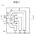
- a conductor of a electrode layer 15 connected either to the front end or rear end of a MR element, and a portion of a bias conductor (16) are included in a conductive pattern 17, and a terminal connected to the conductive pattern 17 is grounded.
- a thin film head 11 of such a construction having a sliding surface a which faces a magnetic recording medium, such as a magnetic disk, is fabricated by forming a MR element 13 on a substrate 12 so as to extend in a direction perpendicular to the sliding surface a, coating the MR element 13 with an insulating layer 14, forming contact holes 14a and 14b in the insulating layer 14 at positions corresponding respectively to the front and rear ends of the MR element 2, and simultaneously forming a rear electrode 15B connected through the contact hole 14b to the rear end of the MR element 13, a bias conductor 16, and a conductive pattern 17 having a portion forming a front electrode, not shown, connected through the contact hole 14a to the MR element 13 and a portion forming a portion of the bias conductor 16 in a single process.
- a portion of the bias conductor 16 included in the conductive pattern 17 extends over and across the MR element 13.
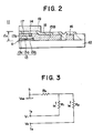
- the MR element 13 is shielded by a magnetic shielding layer 19 formed on an insulating layer 18.
- the MR element 13 consists of two magnetic films 13b and 13c and a nonmagnetic intermediate layer 13a formed between the two magnetic films 13b and 13c.
- Such a construction of the MR element 13 suppresses the generation of Barkhausen noise, i.e., noise attributable to domain wall replacement.
- the front end of the MR element 13, and a portion of the conductive pattern 17 corresponding to the front end of the MR element 13 are exposed in the sliding surface a.
- a terminal t1 connected to the conductive pattern 17 is connected to a ground potential Vss, a terminal t2 connected to the rear electrode 15B connected to the rear end of the MR element 13 is connected to an amplifier, not shown, to apply a predetermined voltage to the terminal t2 by a constant-voltage power supply. A predetermined voltage is applied to a terminal t3 connected to the bias conductor 16.
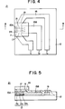
- FIG. 3 shows an equivalent circuit whose behavior is identical with that of the thin film head 11. Referring to Fig.
- R1 represents the resistance of the MR element 13 and the rear electrode 15B
- R2 represents the resistance of the bias conductor 16, i.e., a portion of the bias conductor 16 before the conductive pattern
- R3 represents the resistance of the conductive pattern 17.
- the output variation ⁇ V corresponds to the variation of the potential difference between the terminal t1 connected to the conductive pattern 17 and the terminal t2 connected to the rear electrode 15B of the MR element 13 when the current is maintained constant.
- that flows through the conductive pattern 17 having the resistance R3 can be reduced to suppress the generation of heat and noise.
- the thin film head 11 In fabricating the thin film head 11, the electrodes of the MR element 13, and the bias conductor are formed simultaneously by a single process, the thin film head 11 can be formed in a simple layered construction and has a small gap l3. Since the front electrode of the MR element 13 and a portion of the bias conductor are included in the conductive pattern 17, a portion 17a of the conductive pattern 17 in contact with the front end of the MR element 13, and a contact portion 17b of the conductive pattern 17 in contact with the the rear end of the MR element 13, i.e., a portion of the rear electrode 15B in contact with the MR element 13, can be formed in a sufficiently large contact area even if the MR element 13 is formed in a comparatively small size to deal with high-density recording.
- the construction of the thin film head thus fabricated prevents layer short between the electrode layer for the MR element 13, and the bias conductor, which enhances the reliability of the thin film head. Furthermore, the thin film head in accordance with the present invention has three terminal where as the conventional thin film head has four terminals.
- Figs. 4 and 5 show a thin film head 21 in second embodiment according to the present invention.
- a slit 22 is formed in the conductive pattern 17 of the thin film head 21 to separate a portion 15A of the conductive pattern 17 serving as the front electrode of the MR element 13, and a portion 16a of the conductive pattern 17 serving as a bias conductor from each other and to join the portion 15A to a bias conductor 16 at a junction p at a position outside an area corresponding to the MR element 13 so that a sense current i S and a bias current i B join at a position outside the area corresponding to the MR element 13.
- the bias current i B is not disturbed while the same flows over the MR element 13, so that a bias magnetic field can further satisfactorily be applied to the MR element 13. Since the conductive portions 15A and the bias conductor 16 joins at a position very close to the MR element 13, increase in the resistance of the conductive portion 15A connected to the front end of the MR element 13 is insignificant.
- the thin film head 21 has the same advantages as those of the thin film head 11 shown in Fig. 1.
- Fig. 6 shows a thin film head 23 in a third embodiment according to the present invention.
- the thin film head 23 is identical in construction with the thin film head 11 shown in Fig. 1, except that, in the thin film head 23, a portion of a rear electrode 15B connected to the rear end of a MR element 13 and a portion of a bias conductor 16 are included in a conductive pattern 24, and a terminal t4 is connected to the conductive pattern 24 as a common terminal for the rear electrode 15B and the bias conductor 16.
- Fig. 7 shows an equivalent circuit whose behavior is identical with that of the thin film head 23. In Fig. 7, resistances R1, R2 and R3 corresponds respectively to those in Fig.
- R4 represents the resistance of a portion of the conductive pattern 24 serving as the rear electrode.
- the thin film head 23 does not allow the individual selection of a bias current i B to be supplied to the bias conductor 16 and a sense current i S to be supplied to the MR element 13, the thin film head 23 has only two terminals t1 and t4. Other advantages of the thin film head 23 are the same as those of the thin film head 11 shown in Fig. 1.
- Figs. 8 and 9 shows a thin film head 25 in a fourth embodiment according to the present invention.
- the thin film head 25 is capable of functioning at a high reliability under high-temperature, high-humidity environmental conditions.
- the thin film head 25 has an electrode layer 15 for a MR element 13, consisting of a metal layer having a comparatively small resistivity and a moisture-resistant conductive layer, and a portion of the electrode layer contiguous with the sliding surface a of the thin film head 25 is formed only of a portion of the moisture-resistant conductive layer.
- the MR element 13 of the said two-layer construction is formed on a substrate so as to extend in a direction perpendicular to the sliding surface.
- An electrode layer 15 for supplying, a sense current i S to the MR element in the direction of a signal magnetic field has a front electrode 15A connected to the front end of the MR element 13 and a rear electrode 15B connected to the rear end of the MR element 13.
- a bias conductor 16 is formed so as to extend across the MR element 13 on an insulating layer 14 covering the MR element 13.
- a magnetic shielding layer 19 is formed on an insulating layer 18 so as to shield the MR element 13.
- the front electrode 15A and the rear electrode 15B connected to the MR element 13 consist of a moisture-resistant conductive layer 26 formed of a moisture-resistant material, such as Ti, Mo, W, Cr, SuS or C, and a principal conductive layer 27 formed of a metal having a comparatively small resistivity, such as Cu, Au or Al. If the principal conductive layer 27 is formed of a metal having an inferior adhesive property, such as Au, a bonding metal layer 28, such as a Ti layer or a Mo layer, is formed on the principal conductive layer 27. A portion of the front electrode 15A contiguous with the sliding surface a, namely, a portion extending as deep as 0.5 ⁇ m or above from the sliding surface a, is formed only of the moisture-resistant conductive layer 26.
- a moisture-resistant conductive layer 26 formed of a moisture-resistant material, such as Ti, Mo, W, Cr, SuS or C
- a principal conductive layer 27 formed of a metal having a comparatively small resistivity, such as Cu, Au or
- a portion of the front electrode 15A connected to the MR element 13 is formed only of the moisture-resistant conductive layer 26.
- the bias conductor 16 may be the same laminated metal layer as that forming the electrodes 15A and 15B.
- the front electrode 15A can readily be formed by a process comprising steps of sequentially forming the moisture-resistant conductive layer 26, the principal conductive layer 27 and the bonding metal layer 28 in that order in the shape of the electrode on the insulating layer 14 including a contact hole, etching a portion of the superposed bonding metal layer 28 contiguous with the sliding surface a and connected to the MR element 13, and a portion of the principal conductive layer 27 corresponding to that of the bonding metal layer 28 by ion milling using a resist mask, and stopping the etching operation upon the exposure of the moisture-resistant layer 26.
- the front electrode 15A excluding a portion thereof contiguous with the sliding surface a is formed of the principal conductive layer 27 and the moisture-resistant layer, and only the moisture-resistant layer 26 of the front electrode 15A is exposed in the sliding surface a, the front electrode 15A exposed in the sliding surface a is not deteriorated by oxidation and corrosion even if the thin film head 25 is used under high-temperature, high-humidity conditions, so that the thin film head 25 maintains its high reliability.
- Figs. 10 and 11 are graphs showing results of environmental tests respectively of the thin film head in the fourth embodiment according to the present invention provided with a Ti film as the moisture-resistant layer 26, and a conventional thin film head under high-temperature, high-humidity (temperature: 60°C, humidity: 90%) conditions.
- the resistance of the MR element of the conventional thin film head between the electrodes increases sharply with time, which proves that the electrodes are deteriorated by corrosion.
- a curve I in Fig. 10 the resistance of the MR element of the thin film head of the present invention between the electrodes remains substantially constant for a long time, which proves that the electrodes are not deteriorated.
- a straight line II indicates a fraction nondefective.
- the thin film head of the present invention is capable of enduring long service under high-temperature, high-humidity conditions.
- the techniques applied to the thin film head 25 can be applied also to the thin film heads 11, 12 and 23.
- the present invention is applicable also to a double-shielded thin film head provided with a MR element having upper and lower sides shielded magnetic shielding layers, respectively.
- the gap of the magnetoresistance-effect thin film head in the first aspect of the present invention can readily be formed in a reduced size even if the MR element is formed in a reduced size to cope with high-density recording by forming a conductive layer so as to include a portion of the electrode connected to the MR element, and a portion of the bias magnetic field creating conductor.
- Such a construction of the magnetoresistance-effect thin film head enables the uniform application of a bias magnetic field to the MR element, reduces the number of external terminals, prevents layer short between the electrodes of the MR element and the bias magnetic field creating layer, and enhances the reliability of the magnetoresistance-effect thin film head.
- the electrode having a portion contiguous with the sliding surface and formed of a moisture-resistant material employed as the front electrode of the MR element of the magnetoresistance-effect thin film head in the second aspect of the present invention is free from deterioration even if the magnetoresistance-effect thin film head is used under high-temperature, high-humidity conditions, which ensures the high reliability of the magnetoresistance-effect effect thin film head.
Landscapes
- Engineering & Computer Science (AREA)
- Manufacturing & Machinery (AREA)
- Magnetic Heads (AREA)
Claims (2)
- Magnetkopf (11) nach dem Magnetwiderstandseffekt in Dünnfilmtechnik mit:einem Substrat (12);einem Magnetfeldmeßfühler (13) auf dem Substrat (12);einer Elektrodenschlcht (15) mit sich jeweils von entgegengesetzten Seiten des Magnetfeldmeßfühlers (13) ausdehnenden Bereichen, um einen Lesestrom an den Magnetfeldmeßfühler (13) so anzulegen, daß er in Richtung eines magnetischen Nutzfeldes fließt;einer über dem Magnetfeldmeßfühler (13) ausgebildeten Isolierschicht (14);einem auf der Isolierschicht (14) ausgebildeten ein Vormagnetisierungsfeld erzeugenden Leiter (16), der sich quer über den Magnetfeldmeßfühler (13) ausdehnt; undeiner den Magnetfeldmeßfühler (13) abschirmenden magnetischen Abschirmschicht (19);dadurch gekennzeichnet, daß mindestens ein Bereich der Elektrodenschicht (15) und ein Bereich des das Vormagnetisierungsfeld erzeugenden Leiters (16) in einem leitenden Muster (17) enthalten sind.
- Magnetkopf nach Anspruch 1, dadurch gekennzeichnet, daß die Elektrodenschicht (15) aus einem zumindest relativ gut leitenden Metallleiter (27) und einem feuchtigkeitsbeständigen Leiter (26) besteht, und daßein Bereich der Elektrodenschicht (15) anschließend an die Gleltfläche aus dem feuchtigkeitsbeständigen Leiter (26) gebildet ist.
Applications Claiming Priority (2)
| Application Number | Priority Date | Filing Date | Title |
|---|---|---|---|
| JP2140685A JPH0434713A (ja) | 1990-05-30 | 1990-05-30 | 磁気抵抗効果型薄膜ヘッド |
| JP140685/90 | 1990-05-30 |
Publications (3)
| Publication Number | Publication Date |
|---|---|
| EP0459404A2 EP0459404A2 (de) | 1991-12-04 |
| EP0459404A3 EP0459404A3 (en) | 1992-01-15 |
| EP0459404B1 true EP0459404B1 (de) | 1996-01-24 |
Family
ID=15274376
Family Applications (1)
| Application Number | Title | Priority Date | Filing Date |
|---|---|---|---|
| EP91108704A Expired - Lifetime EP0459404B1 (de) | 1990-05-30 | 1991-05-28 | Magnetwiderstandseffekt-Dünnfilmkopf |
Country Status (4)
| Country | Link |
|---|---|
| US (1) | US5351158A (de) |
| EP (1) | EP0459404B1 (de) |
| JP (1) | JPH0434713A (de) |
| DE (1) | DE69116602T2 (de) |
Families Citing this family (23)
| Publication number | Priority date | Publication date | Assignee | Title |
|---|---|---|---|---|
| JPH0434713A (ja) * | 1990-05-30 | 1992-02-05 | Sony Corp | 磁気抵抗効果型薄膜ヘッド |
| US5682284A (en) * | 1992-08-25 | 1997-10-28 | Seagate Technology, Inc. | Read sensitivity function for barberpole bias design magnetoresistive sensor having curved current contacts |
| JPH06251339A (ja) * | 1993-02-26 | 1994-09-09 | Sony Corp | 磁気抵抗効果型薄膜磁気ヘッド及びバイアス特性測定方法 |
| US5644228A (en) * | 1993-08-31 | 1997-07-01 | Eastman Kodak Company | Permanent magnet assembly with MR and DC compensating bias |
| KR950012334A (ko) * | 1993-10-29 | 1995-05-16 | 윌리엄 티. 엘리스 | 자기 저항 헤드 어셈블리 및 자기 저항 헤드를 정전하 방전으로부터 보호하는 방법 |
| US5438470A (en) * | 1994-05-13 | 1995-08-01 | Read-Rite Corporation | Magnetoresistive structure with contiguous junction hard bias design with low lead resistance |
| TW248602B (en) * | 1994-05-31 | 1995-06-01 | Ibm | Magnetoresistive head with asymmetric leads |
| US5557491A (en) * | 1994-08-18 | 1996-09-17 | International Business Machines Corporation | Two terminal single stripe orthogonal MR head having biasing conductor integral with the lead layers |
| JP3045942B2 (ja) * | 1994-12-07 | 2000-05-29 | アルプス電気株式会社 | 薄膜磁気ヘッド |
| JPH08203037A (ja) * | 1995-01-31 | 1996-08-09 | Sony Corp | 磁気抵抗効果型磁気ヘッド |
| US5867350A (en) * | 1995-03-29 | 1999-02-02 | Sony Corporation | Magneto-resistance effect head with insulated bias conductor embedded in shield groove |
| JPH0916916A (ja) * | 1995-06-29 | 1997-01-17 | Sony Corp | 薄膜磁気ヘッド及びその製造方法 |
| EP0770991A3 (de) * | 1995-10-26 | 1998-05-20 | Read-Rite Corporation | Dünnfilmmagnetoresistiver Kopf mit aneinandergrenzendem Übergang |
| JPH09293217A (ja) * | 1996-04-26 | 1997-11-11 | Fujitsu Ltd | 磁気抵抗効果型ヘッド |
| US5930084A (en) * | 1996-06-17 | 1999-07-27 | International Business Machines Corporation | Stabilized MR sensor and flux guide joined by contiguous junction |
| US6064551A (en) * | 1997-02-27 | 2000-05-16 | Sony Corporation | Magnetoresistance effect type magnetic head |
| JP2924845B2 (ja) * | 1997-03-24 | 1999-07-26 | ティーディーケイ株式会社 | スピンバルブ磁気抵抗素子を備えた磁気ヘッド及びその製造方法 |
| US5792380A (en) * | 1997-04-30 | 1998-08-11 | Eastman Kodak Company | Ink jet printing ink composition with detectable label material |
| JP2000030222A (ja) * | 1998-07-08 | 2000-01-28 | Fujitsu Ltd | 磁気センサ |
| JP2000242911A (ja) * | 1999-02-22 | 2000-09-08 | Tdk Corp | 複合型薄膜磁気ヘッドの製造方法 |
| JP3389892B2 (ja) * | 1999-09-24 | 2003-03-24 | 株式会社村田製作所 | ヘッド |
| US7009818B1 (en) * | 2002-12-30 | 2006-03-07 | Storage Technology Corporation | Thin film magnetic head having improved thermal characteristics, and method of manufacturing |
| US7719802B2 (en) * | 2003-09-23 | 2010-05-18 | Seagate Technology Llc | Magnetic sensor with electrically defined active area dimensions |
Family Cites Families (15)
| Publication number | Priority date | Publication date | Assignee | Title |
|---|---|---|---|---|
| JPS584992A (ja) * | 1981-07-01 | 1983-01-12 | Hitachi Ltd | 磁気電気変換素子 |
| US4967298A (en) * | 1987-02-17 | 1990-10-30 | Mowry Greg S | Magnetic head with magnetoresistive sensor, inductive write head, and shield |
| US5159511A (en) * | 1987-04-01 | 1992-10-27 | Digital Equipment Corporation | Biasing conductor for MR head |
| US5081554A (en) * | 1987-04-01 | 1992-01-14 | Digital Equipment Corporation | Biasing conductor for MR head |
| US5103553A (en) * | 1987-07-29 | 1992-04-14 | Digital Equipment Corporation | Method of making a magnetic recording head |
| US5111352A (en) * | 1987-07-29 | 1992-05-05 | Digital Equipment Corporation | Three-pole magnetic head with reduced flux leakage |
| JPS6482311A (en) * | 1987-09-24 | 1989-03-28 | Hitachi Ltd | Magnetic head |
| JP2668897B2 (ja) * | 1987-10-29 | 1997-10-27 | ソニー株式会社 | 磁気抵抗効果型磁気ヘッド |
| JP2596010B2 (ja) * | 1987-10-29 | 1997-04-02 | ソニー株式会社 | 磁気抵抗効果型磁気ヘッド |
| US4914538A (en) * | 1988-08-18 | 1990-04-03 | International Business Machines Corporation | Magnetoresistive read transducer |
| US5005096A (en) * | 1988-12-21 | 1991-04-02 | International Business Machines Corporation | Magnetoresistive read transducer having hard magnetic shunt bias |
| KR940004989B1 (ko) * | 1989-08-04 | 1994-06-09 | 마쯔시다덴기산교 가부시기가이샤 | 박막자기헤드 |
| US4987509A (en) * | 1989-10-05 | 1991-01-22 | Hewlett-Packard Company | Magnetoresistive head structures for longitudinal and perpendicular transition detection |
| NL8902569A (nl) * | 1989-10-17 | 1991-05-16 | Philips Nv | Dunnefilm magneetkop. |
| JPH0434713A (ja) * | 1990-05-30 | 1992-02-05 | Sony Corp | 磁気抵抗効果型薄膜ヘッド |
-
1990
- 1990-05-30 JP JP2140685A patent/JPH0434713A/ja active Pending
-
1991
- 1991-05-28 EP EP91108704A patent/EP0459404B1/de not_active Expired - Lifetime
- 1991-05-28 US US07/706,257 patent/US5351158A/en not_active Expired - Fee Related
- 1991-05-28 DE DE69116602T patent/DE69116602T2/de not_active Expired - Fee Related
Also Published As
| Publication number | Publication date |
|---|---|
| EP0459404A2 (de) | 1991-12-04 |
| DE69116602T2 (de) | 1996-09-05 |
| EP0459404A3 (en) | 1992-01-15 |
| JPH0434713A (ja) | 1992-02-05 |
| US5351158A (en) | 1994-09-27 |
| DE69116602D1 (de) | 1996-03-07 |
Similar Documents
| Publication | Publication Date | Title |
|---|---|---|
| US5351158A (en) | Magnetoresistance effect thin film head with interconnected electrode structure | |
| US5272582A (en) | Magneto-resistance effect magnetic head with static electricity protection | |
| US5805390A (en) | Method of fabricating magnetoresistive effect type magnetic head capable of preventing electrostatic damage | |
| EP0534791B1 (de) | Magnetowiderstandseffekt-Dünnfilmmagnetkopf | |
| US5978181A (en) | Magnetic head and magnetic recording/reproducing apparatus | |
| EP0269129B1 (de) | Dünnfilmmagnetkopf | |
| US5097372A (en) | Thin film magnetic head with wide recording area and narrow reproducing area | |
| EP0475397A2 (de) | Flächenförmiger dünnschichtiger Magnetkopf | |
| CA1182905A (en) | Magnetic transducer head utilizing magnetoresistance effect | |
| EP0107982B1 (de) | Magnetwandlerköpfe, die einen Magnetwiderstand-Effekt verwenden | |
| EP0204902A2 (de) | Magnetischer Wandlerkopf mit Joch und Nutzung eines Magnetwiderstandseffekts | |
| US6191925B1 (en) | Dual element read with shaped elements | |
| EP0457278B1 (de) | Magnetowiderstandseffekt-Dünnfilmmagnetkopf | |
| US5958612A (en) | Magnetoresistive read transducer | |
| US6671137B2 (en) | Magnetoresistive head including earth members | |
| KR100280300B1 (ko) | 조합된 판독/기입 자기 헤드 | |
| US5966274A (en) | Magneto-resistive magnetic head with track width defined by oppositely positioned recesses and manufacturing method therefor | |
| US5621593A (en) | Magnetoresistive head and method of fabricating the same | |
| DE69421556T2 (de) | Magnetowiderstanddünnfilmmagnetkopf | |
| EP0549031B1 (de) | Dünnfilm-Magnetkopf mit Polymer auf unterbrochenen Flussleiterabschnitten, Produktionsverfahren und integrierte Struktur dasselbe enthaltend | |
| EP0482642A2 (de) | Zusammengesetzter magnetoresistiver Dünnfilmmagnetkopf | |
| JPH04137212A (ja) | 磁気抵抗効果磁気ヘッド | |
| JPH05151533A (ja) | 磁気抵抗効果型薄膜ヘツド | |
| JPH02239951A (ja) | 画像記録ヘッドと、その製造方法と、画像記録ヘッドを用いた画像記録装置と、画像記録ヘッドの実装装置 | |
| JPS622363B2 (de) |
Legal Events
| Date | Code | Title | Description |
|---|---|---|---|
| PUAI | Public reference made under article 153(3) epc to a published international application that has entered the european phase |
Free format text: ORIGINAL CODE: 0009012 |
|
| PUAL | Search report despatched |
Free format text: ORIGINAL CODE: 0009013 |
|
| AK | Designated contracting states |
Kind code of ref document: A2 Designated state(s): DE FR GB |
|
| AK | Designated contracting states |
Kind code of ref document: A3 Designated state(s): DE FR GB |
|
| 17P | Request for examination filed |
Effective date: 19920617 |
|
| 17Q | First examination report despatched |
Effective date: 19941024 |
|
| GRAA | (expected) grant |
Free format text: ORIGINAL CODE: 0009210 |
|
| AK | Designated contracting states |
Kind code of ref document: B1 Designated state(s): DE FR GB |
|
| REF | Corresponds to: |
Ref document number: 69116602 Country of ref document: DE Date of ref document: 19960307 |
|
| ET | Fr: translation filed | ||
| PLBE | No opposition filed within time limit |
Free format text: ORIGINAL CODE: 0009261 |
|
| STAA | Information on the status of an ep patent application or granted ep patent |
Free format text: STATUS: NO OPPOSITION FILED WITHIN TIME LIMIT |
|
| 26N | No opposition filed | ||
| PGFP | Annual fee paid to national office [announced via postgrant information from national office to epo] |
Ref country code: FR Payment date: 20010518 Year of fee payment: 11 |
|
| PGFP | Annual fee paid to national office [announced via postgrant information from national office to epo] |
Ref country code: DE Payment date: 20010522 Year of fee payment: 11 |
|
| PGFP | Annual fee paid to national office [announced via postgrant information from national office to epo] |
Ref country code: GB Payment date: 20010523 Year of fee payment: 11 |
|
| REG | Reference to a national code |
Ref country code: GB Ref legal event code: IF02 |
|
| PG25 | Lapsed in a contracting state [announced via postgrant information from national office to epo] |
Ref country code: GB Free format text: LAPSE BECAUSE OF NON-PAYMENT OF DUE FEES Effective date: 20020528 |
|
| PG25 | Lapsed in a contracting state [announced via postgrant information from national office to epo] |
Ref country code: DE Free format text: LAPSE BECAUSE OF NON-PAYMENT OF DUE FEES Effective date: 20021203 |
|
| GBPC | Gb: european patent ceased through non-payment of renewal fee |
Effective date: 20020528 |
|
| PG25 | Lapsed in a contracting state [announced via postgrant information from national office to epo] |
Ref country code: FR Free format text: LAPSE BECAUSE OF NON-PAYMENT OF DUE FEES Effective date: 20030131 |
|
| REG | Reference to a national code |
Ref country code: FR Ref legal event code: ST |