EP0458244A2 - Cell library method for semiconductor integrated circuit design - Google Patents
Cell library method for semiconductor integrated circuit design Download PDFInfo
- Publication number
- EP0458244A2 EP0458244A2 EP91108148A EP91108148A EP0458244A2 EP 0458244 A2 EP0458244 A2 EP 0458244A2 EP 91108148 A EP91108148 A EP 91108148A EP 91108148 A EP91108148 A EP 91108148A EP 0458244 A2 EP0458244 A2 EP 0458244A2
- Authority
- EP
- European Patent Office
- Prior art keywords
- cell
- power source
- cmos
- source wires
- bicmos
- Prior art date
- Legal status (The legal status is an assumption and is not a legal conclusion. Google has not performed a legal analysis and makes no representation as to the accuracy of the status listed.)
- Granted
Links
- 239000004065 semiconductor Substances 0.000 title claims abstract description 14
- 238000000034 method Methods 0.000 title description 13
- 239000000758 substrate Substances 0.000 description 6
- 230000004048 modification Effects 0.000 description 2
- 238000012986 modification Methods 0.000 description 2
- 230000006978 adaptation Effects 0.000 description 1
- 238000010586 diagram Methods 0.000 description 1
Images


Classifications
-
- H—ELECTRICITY
- H01—ELECTRIC ELEMENTS
- H01L—SEMICONDUCTOR DEVICES NOT COVERED BY CLASS H10
- H01L27/00—Devices consisting of a plurality of semiconductor or other solid-state components formed in or on a common substrate
- H01L27/02—Devices consisting of a plurality of semiconductor or other solid-state components formed in or on a common substrate including semiconductor components specially adapted for rectifying, oscillating, amplifying or switching and having potential barriers; including integrated passive circuit elements having potential barriers
- H01L27/04—Devices consisting of a plurality of semiconductor or other solid-state components formed in or on a common substrate including semiconductor components specially adapted for rectifying, oscillating, amplifying or switching and having potential barriers; including integrated passive circuit elements having potential barriers the substrate being a semiconductor body
- H01L27/10—Devices consisting of a plurality of semiconductor or other solid-state components formed in or on a common substrate including semiconductor components specially adapted for rectifying, oscillating, amplifying or switching and having potential barriers; including integrated passive circuit elements having potential barriers the substrate being a semiconductor body including a plurality of individual components in a repetitive configuration
- H01L27/118—Masterslice integrated circuits
- H01L27/11896—Masterslice integrated circuits using combined field effect/bipolar technology
Definitions
- This invention relates to a cell library for a semiconductor integrated circuit design, more particularly a cell library for gate array or standard cell including BiCMOS cells.
- the first is the method wherein all processes, from positioning the elements to the wiring for a transistor or the like, are performed anew each time on a semiconductor substrate. This is known as the full custom method and exhibits the features of high performance and good efficiency in forming a small chip. On the other hand, this method has the drawback that development requires a long time and much labor.
- the second method is the opposite of the first, in as much as the elements of the transistor or the like are provided in advance in the form of an array on the substrate of the semiconductor, already prepared as a wafer, and only the wiring between the elements must be decided, according to the application.
- This is referred to as the gate array method.
- the wiring for forming the necessary blocks (cells) to provide the various functions using this array is designed in advance and preperated in the form of a library. The designer combines the appropriate cells with reference to the library, and designs the intercell wiring. Following this, the actual wiring is done to required with this method is extremely short.
- the third method known as the standard cell method.
- the arrangement of the elements and the wiring within one cell are designed as the optimum for each cell, and the designer, as a result, requires a shorter development period than for the full custom because only the combining of the cells and their interwiring need be performed.
- the arrangement of the cells on the semiconductor substrate from the stage of preparing the wafer, and more time is required to complete the LSI than for the gate array.
- a conventional CMOS gate array or CMOS standard cell is illustrated in Fig. 1.
- a basic cell 101 is arranged to form a plurality of rows between which a wiring field 103 is interposed.
- a power source wiring 105 and a power source wiring 107 are formed on the upper and lower ends respectively of the individual cells, and the power wiring is connected automatically between the sudjoining cells so that two series of power wiring 105 and 107 are formed, running through the respective rows.
- the utilization of the design method is limited to the circuitry around which the CMOS is centered. If a decision is made to use a circuit including a bipolar element (BiCMOS) as a gate array or standard cell, respectively, in the case where a bipolar element is incorporated in the cell, one cell becomes rather large in size. To add this cell with a bipolar element to a conventional library, certain means are required. In the most common means considered, the design is modified to adapt each cell of a CMOS library to the BiCMOS size.
- BiCMOS bipolar element
- An object of the present invention is to provide a cell library including CMOS cells, BiCMOS cells, and cells each of which has a CMOS cell and a BiCMOS cell for a semiconductor integrated circuit design.
- the cell library for a semiconductor integrated circuit design which is one aspect according to the present invention, comprises CMOS cell comprising two power source wires and a CMOS circuit placed between the two power source wires with a predetermined distance, and a BiCMOS cell comprising two power source wires which are placed at a distance equal to the distance between the power source wires in the CMOS cell, a CMOS circuit placed between the two power source wires in the BiCMOS cell, and bipolar transistor circuits placed at both outsides of the two power source wires in the BiCMOS cell.
- a cell library which is another aspect according to the present invention comprises CMOS cell comprising two power source wires and a CMOS circuit placed between the two power source wires with a predetermined distance, BiCMOS cell comprising two power source wires which are placed at a distance which is longer than the distance between the power source wires in the CMOS cell, a CMOS circuit placed between the two power source wires in the BiCMOS cell, and bipolar transistor circuits placed at both insides of the two power source wires in the BiCMOS cell, and two power source wires for connecting the two power source wires in the CMOS cell to the power source wires in the BiCMOS cell.
- Fig. 2 illustrates the configuration of an integrated circuit using a cell library as a first embodiment of the present invention.
- This circuit can be applied in the case of both a gate array and a standard cell.
- a gate array a plurality of elements is methodically formed in rows on a semiconductor substrate 1 and the function of each cell is provided by then forming the appropriate wiring.
- the arrangement of the elements on the semiconductor substrate is determined for each cell.
- a plurality of CMOS cells 3 is provided.
- Each CMOS cell 3 comprises a 5V power wire 5 and a 0 V power wire, specifically, a ground wire 7, and a CMOS circuit 9, formed between the power wire 5 and the ground wire 7.
- a BiCMOS cell 11 comprises the power wire 15, the ground wire 17, and a CMOS circuit 13 formed between the power wire 5 and the ground wire 7.
- bipolar transistor circuits 14 are provided external to the power wire 15 and the ground wire 7. All the power wires 15 and the ground wires 17 are formed at the same height so that if the CMOS cells 3 and the BiCMOS cell 11 are lined up in a row as shown in the drawing, the power wires 5 and 15 and the ground wires 7 and 17 are all formed running in common.
- An interval between the adjacent cell rows is a wiring field to connect these cells.
- CMOS cells only the part of the BiCMOS cell which extends outside of the power wires and the ground wires (a bipolar transistor circuits 14, 16) infringes on the area of the wiring field.
- the circuit actually occupied by the BiCMOS is only about 10 % of the total area, so this does not become a problem.
- the elements are also formed in the wiring field 10.
- the CMOS and the bipolar transistor and the like take up the entire semiconductor substrate. Specifically, a row 21 in which an NMOS row 37, a PMOS row 39, a bipolar transistor, and a resistance are lined up in that order and methodically repeated is formed. A PMOS transistor P, an NMOS transistor N, a bipolar transistor B, and a resistance I are respectively shown in Fig. 3. The same reference numerals are used for the power wires, the CMOS cell, and the BiCMOS cell as in Fig. 2.
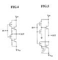
- This type of cell library is design in the case where bipolar transistors are used on the output part OUT of a logic circuit shown in Fig. 4 and Fig. 5.
- Fig. 6 shows a second embodiment of the present invention.
- all the elements of a BiCMOS cell 23 are formed between a power wire 25 and a ground wire 27.
- a power wire 31 and a ground wire 33 are formed running completely on the outside of a CMOS cell 29.
- the power wire 25 can be connected to the power wire 31 and the ground wire 27 can be connected to the ground wire 33 by preparing a connecting cell 30 having two connecting wires 135 and 137.
- connecting wires 135 and 137 for connecting the wires 25 and 27 in the CMOS cell to the wires 31 and 33 in the BiCMOS cell as shown in Fig. 7 can also be provided between the CMOS cell 29 and the BiCMOS cell 23 instead of the connecting cell 30 shown in Fig. 6.
- CMOS cell library of the present invention can be used without modification.
Landscapes
- Engineering & Computer Science (AREA)
- Power Engineering (AREA)
- Physics & Mathematics (AREA)
- Condensed Matter Physics & Semiconductors (AREA)
- General Physics & Mathematics (AREA)
- Computer Hardware Design (AREA)
- Microelectronics & Electronic Packaging (AREA)
- Design And Manufacture Of Integrated Circuits (AREA)
Abstract
Description
- This invention relates to a cell library for a semiconductor integrated circuit design, more particularly a cell library for gate array or standard cell including BiCMOS cells.
- There are three types of conventional design methods for LSIs.
- The first is the method wherein all processes, from positioning the elements to the wiring for a transistor or the like, are performed anew each time on a semiconductor substrate. this is known as the full custom method and exhibits the features of high performance and good efficiency in forming a small chip. On the other hand, this method has the drawback that development requires a long time and much labor.
- The second method is the opposite of the first, in as much as the elements of the transistor or the like are provided in advance in the form of an array on the substrate of the semiconductor, already prepared as a wafer, and only the wiring between the elements must be decided, according to the application. This is referred to as the gate array method. The wiring for forming the necessary blocks (cells) to provide the various functions using this array is designed in advance and preperated in the form of a library. The designer combines the appropriate cells with reference to the library, and designs the intercell wiring. Following this, the actual wiring is done to required with this method is extremely short.
- Intermediate to these two methods is the third method, known as the standard cell method. In this case, the arrangement of the elements and the wiring within one cell are designed as the optimum for each cell, and the designer, as a result, requires a shorter development period than for the full custom because only the combining of the cells and their interwiring need be performed. However, the arrangement of the cells on the semiconductor substrate from the stage of preparing the wafer, and more time is required to complete the LSI than for the gate array.
- A conventional CMOS gate array or CMOS standard cell is illustrated in Fig. 1. A
basic cell 101 is arranged to form a plurality of rows between which awiring field 103 is interposed. Apower source wiring 105 and apower source wiring 107 are formed on the upper and lower ends respectively of the individual cells, and the power wiring is connected automatically between the sudjoining cells so that two series ofpower wiring - In the development of conventional gate array or standard cells as described above, the utilization of the design method is limited to the circuitry around which the CMOS is centered. If a decision is made to use a circuit including a bipolar element (BiCMOS) as a gate array or standard cell, respectively, in the case where a bipolar element is incorporated in the cell, one cell becomes rather large in size. To add this cell with a bipolar element to a conventional library, certain means are required. In the most common means considered, the design is modified to adapt each cell of a CMOS library to the BiCMOS size.
- However, in this case the entire cell library must be rebuilt, which necessitates a great deal of time and trouble. Furthermore, the necessity is produced for separately administering a library for CMOS use and a library for BiCMOS use, which is very inefficient.
- An object of the present invention is to provide a cell library including CMOS cells, BiCMOS cells, and cells each of which has a CMOS cell and a BiCMOS cell for a semiconductor integrated circuit design.
- The cell library for a semiconductor integrated circuit design which is one aspect according to the present invention, comprises CMOS cell comprising two power source wires and a CMOS circuit placed between the two power source wires with a predetermined distance, and a BiCMOS cell comprising two power source wires which are placed at a distance equal to the distance between the power source wires in the CMOS cell, a CMOS circuit placed between the two power source wires in the BiCMOS cell, and bipolar transistor circuits placed at both outsides of the two power source wires in the BiCMOS cell.
- A cell library which is another aspect according to the present invention comprises CMOS cell comprising two power source wires and a CMOS circuit placed between the two power source wires with a predetermined distance, BiCMOS cell comprising two power source wires which are placed at a distance which is longer than the distance between the power source wires in the CMOS cell, a CMOS circuit placed between the two power source wires in the BiCMOS cell, and bipolar transistor circuits placed at both insides of the two power source wires in the BiCMOS cell, and two power source wires for connecting the two power source wires in the CMOS cell to the power source wires in the BiCMOS cell.
- These and other objects, feature and advantages of the present invention will be more apparent from the following description of a preferred embodiment, taken in conjunction with the accompanying drawing.
-
- Fig. 1 is a plan view of a conventional integrated circuit in which conventional CMOS cells are used;
- Fig. 2 is a plan view of an integrated circuit in which BiCMOS cell and CMOS cell in a cell library according to the present invention are used;
- Fig. 3 is a plan view of a sea of gate array cell according to the present invention;
- Figs. 4 and 5 are circuit diagrams of a conventional inverter;
- Fig. 6 is a plan view of an integrated circuit in which another type BiCMOS cell, CMOS cell, and a connecting cell in a cell library according to the present invention are used; and
- Fig. 7 is a plan view of an integrated circuit in which another type BiCMOS cell and CMOS cells in a cell library according to the present invention are used.
- Fig. 2 illustrates the configuration of an integrated circuit using a cell library as a first embodiment of the present invention. This circuit can be applied in the case of both a gate array and a standard cell. Specifically, in the case of a gate array, a plurality of elements is methodically formed in rows on a
semiconductor substrate 1 and the function of each cell is provided by then forming the appropriate wiring. In the case of a standard cell the arrangement of the elements on the semiconductor substrate is determined for each cell. - A plurality of
CMOS cells 3 is provided. EachCMOS cell 3 comprises a5V power wire 5 and a 0 V power wire, specifically, aground wire 7, and a CMOS circuit 9, formed between thepower wire 5 and theground wire 7. A BiCMOScell 11 comprises thepower wire 15, theground wire 17, and aCMOS circuit 13 formed between thepower wire 5 and theground wire 7. In addition to these,bipolar transistor circuits 14 are provided external to thepower wire 15 and theground wire 7. All thepower wires 15 and theground wires 17 are formed at the same height so that if theCMOS cells 3 and theBiCMOS cell 11 are lined up in a row as shown in the drawing, thepower wires ground wires - An interval between the adjacent cell rows is a wiring field to connect these cells. As can be clearly understood from the drawing, as compared to the case where the CMOS cells only are formed, only the part of the BiCMOS cell which extends outside of the power wires and the ground wires (a
bipolar transistor circuits 14, 16) infringes on the area of the wiring field. However, the circuit actually occupied by the BiCMOS is only about 10 % of the total area, so this does not become a problem. - A specific example of the adaptation of a gate array known as a sea of gate array to the present invention will now be explained.
- With this type of array, the elements are also formed in the
wiring field 10. As known in Fig. 3, the CMOS and the bipolar transistor and the like take up the entire semiconductor substrate. Specifically, a row 21 in which an NMOS row 37, a PMOS row 39, a bipolar transistor, and a resistance are lined up in that order and methodically repeated is formed. A PMOS transistor P, an NMOS transistor N, a bipolar transistor B, and a resistance I are respectively shown in Fig. 3. The same reference numerals are used for the power wires, the CMOS cell, and the BiCMOS cell as in Fig. 2. - This type of cell library is design in the case where bipolar transistors are used on the output part OUT of a logic circuit shown in Fig. 4 and Fig. 5.
- Fig. 6 shows a second embodiment of the present invention. Here, all the elements of a BiCMOS
cell 23 are formed between apower wire 25 and aground wire 27. In addition, apower wire 31 and aground wire 33 are formed running completely on the outside of aCMOS cell 29. - The
power wire 25 can be connected to thepower wire 31 and theground wire 27 can be connected to theground wire 33 by preparing a connectingcell 30 having two connectingwires - To obtain the same effect of the embodiment as shown in Fig. 6, connecting
wires wires wires CMOS cell 29 and theBiCMOS cell 23 instead of the connectingcell 30 shown in Fig. 6. - Accordingly, in this case also the CMOS cell library of the present invention can be used without modification.
- The preferred embodiments are explained in the foregoing discussion, but the present invention is not limited to these embodiments.
- Various modification will become possible for those skilled in the art after the teaching of the present disclosure without departing from the scope thereof.
- Reference signs in the claims are intended for better understanding and shall not limit the scope.
Claims (4)
- A cell library for a semiconductor integrated circuit design, comprising:
a CMOS cell (3) comprising
two power source wires (5 and 7) and
a CMOS (9) circuit placed between the two power source wires (5 and 7) with a predetermined distance; and
a BiCMOS cell (11) comprising
two power source wires (15 and 17) which are placed at a distance equal to the distance between the power source wires (5 and 7) in the CMOS cell (3),
a CMOS circuit (13) placed between the two power source wires (15 and 17) in the BiCMOS cell (11), and
bipolar transistor circuits (14 and 16) placed at both outsides of the two power source wires (15 and 17) in the BiCMOS cell (11). - A cell library according to claim 1, wherein an output portion of the BiCMOS cell (11) comprises a bipolar transistor circuit (15 and 16).
- A cell library for a semiconductor integrated circuit design, comprising:
a CMOS cell (29) comprising
two power source wires (25 and 27) and
a CMOS circuit placed between the two power source
wires (25 and 29) with a predetermined distance;
a BiCMOS cell (23) comprising
two power source wires (31 and 33) which are placed at a distance which is longer than the distance between the power source wires (25 and 27) in the CMOS cell (29),
a CMOS circuit placed between the two power source wires (31 and 33) in the BiCMOS cell (23), and
bipolar transistor circuits placed at both insides of the two power source wires (31 and 33) in the BiCMOS cell (23),
wherein the two power source wires in the CMOS cell are connected to the power source wires in the BiCMOS cell by two power source wires (35 and 37). - A cell library for a semiconductor integrated circuit design, comprising:
a CMOS cell (29) comprising
two power source wires ( 25 and 27) and
a CMOS circuit placed between the two power source
wires (25 and 29) with a predetermined distance;
a BiCMOS cell (23) comprising
two power source wires (31 and 33) which are placed at a distance which is longer than the distance between the power source wires (25 and 27) in the CMOS cell (29),
a CMOS circuit placed between the two power source wires (31 and 33) in the BiCMOS cell (23), and
bipolar transistor circuits placed at both insides of the two power source wires (31 and 33) in the BiCMOS cell (23); and
a connecting cell (30) having connecting wires (135 and 137) for connecting two power source wires (25 and 27) in the CMOS cell (29) to the power source wires (31 and 33) in the BiCMOS cell (23).
Applications Claiming Priority (2)
| Application Number | Priority Date | Filing Date | Title |
|---|---|---|---|
| JP132497/90 | 1990-05-24 | ||
| JP2132497A JP2505910B2 (en) | 1990-05-24 | 1990-05-24 | Cell library for semiconductor integrated circuits |
Publications (3)
| Publication Number | Publication Date |
|---|---|
| EP0458244A2 true EP0458244A2 (en) | 1991-11-27 |
| EP0458244A3 EP0458244A3 (en) | 1992-01-22 |
| EP0458244B1 EP0458244B1 (en) | 1997-03-19 |
Family
ID=15082757
Family Applications (1)
| Application Number | Title | Priority Date | Filing Date |
|---|---|---|---|
| EP91108148A Expired - Lifetime EP0458244B1 (en) | 1990-05-24 | 1991-05-21 | Cell library method for semiconductor integrated circuit design |
Country Status (5)
| Country | Link |
|---|---|
| US (1) | US5387810A (en) |
| EP (1) | EP0458244B1 (en) |
| JP (1) | JP2505910B2 (en) |
| KR (1) | KR950010202B1 (en) |
| DE (1) | DE69125203T2 (en) |
Cited By (1)
| Publication number | Priority date | Publication date | Assignee | Title |
|---|---|---|---|---|
| CN102142441A (en) * | 2009-12-29 | 2011-08-03 | Nxp股份有限公司 | Flexible CMOS library architecture for leakage power and variability reduction |
Families Citing this family (8)
| Publication number | Priority date | Publication date | Assignee | Title |
|---|---|---|---|---|
| US5798541A (en) * | 1994-12-02 | 1998-08-25 | Intel Corporation | Standard semiconductor cell with contoured cell boundary to increase device density |
| US5682323A (en) | 1995-03-06 | 1997-10-28 | Lsi Logic Corporation | System and method for performing optical proximity correction on macrocell libraries |
| US5768146A (en) * | 1995-03-28 | 1998-06-16 | Intel Corporation | Method of cell contouring to increase device density |
| US5724251A (en) * | 1995-06-07 | 1998-03-03 | Advanced Micro Devices, Inc. | System and method for designing, fabricating and testing multiple cell test structures to validate a cell library |
| GB2384877B (en) * | 2002-02-01 | 2004-12-15 | Micron Technology Inc | System and method for generating high-quality libraries |
| JP4056348B2 (en) * | 2002-10-07 | 2008-03-05 | 株式会社ルネサステクノロジ | Integrated circuit chip module and mobile phone |
| JP2005027041A (en) | 2003-07-02 | 2005-01-27 | Renesas Technology Corp | Solid-state imaging unit |
| JP5918833B1 (en) * | 2014-11-12 | 2016-05-18 | 株式会社ホワイトハウス | Seat rotation device |
Citations (3)
| Publication number | Priority date | Publication date | Assignee | Title |
|---|---|---|---|---|
| JPS5827343A (en) * | 1981-08-10 | 1983-02-18 | Matsushita Electronics Corp | Semiconductor integrated circuit |
| US4575745A (en) * | 1983-06-21 | 1986-03-11 | Rca Corporation | Tailorable standard cells and method for tailoring the performance of IC designs |
| EP0189183A1 (en) * | 1985-01-25 | 1986-07-30 | Hitachi, Ltd. | Semiconducteur integrated circuit device |
Family Cites Families (4)
| Publication number | Priority date | Publication date | Assignee | Title |
|---|---|---|---|---|
| JPH0815209B2 (en) * | 1985-01-25 | 1996-02-14 | 株式会社日立製作所 | Semiconductor integrated circuit device |
| JPH0732194B2 (en) * | 1986-05-23 | 1995-04-10 | 日本電気株式会社 | MOS integrated circuit |
| JPS63197356A (en) * | 1987-02-12 | 1988-08-16 | Matsushita Electric Ind Co Ltd | Integrated circuit device |
| JPH0831581B2 (en) * | 1988-02-19 | 1996-03-27 | 株式会社東芝 | Semiconductor device |
-
1990
- 1990-05-24 JP JP2132497A patent/JP2505910B2/en not_active Expired - Fee Related
-
1991
- 1991-05-15 US US07/699,628 patent/US5387810A/en not_active Expired - Lifetime
- 1991-05-21 EP EP91108148A patent/EP0458244B1/en not_active Expired - Lifetime
- 1991-05-21 DE DE69125203T patent/DE69125203T2/en not_active Expired - Fee Related
- 1991-05-24 KR KR1019910008414A patent/KR950010202B1/en not_active IP Right Cessation
Patent Citations (3)
| Publication number | Priority date | Publication date | Assignee | Title |
|---|---|---|---|---|
| JPS5827343A (en) * | 1981-08-10 | 1983-02-18 | Matsushita Electronics Corp | Semiconductor integrated circuit |
| US4575745A (en) * | 1983-06-21 | 1986-03-11 | Rca Corporation | Tailorable standard cells and method for tailoring the performance of IC designs |
| EP0189183A1 (en) * | 1985-01-25 | 1986-07-30 | Hitachi, Ltd. | Semiconducteur integrated circuit device |
Non-Patent Citations (2)
| Title |
|---|
| PATENT ABSTRACTS OF JAPAN vol. 7, no. 103 (E-173)(1248) 6 May 1983 & JP-A-58 027 343 ( MATSUSHITA DENSHI KOGYO K.K. ) 18 February 1983 * |
| PROCEEDINGS OF THE IEEE 1990 CUSTOM INTEGRATED CIRCUITS CONFERENCE 13 May 1990, BOSTON US T. HANIBUCHI ET AL.: 'A Bipolar-PMOS merged basic cell for 0.8 micron BICMOS Sea-of-Gates' pages 4.2.1-4.2.4' & "BICMOS gate configuration"; firgures 2,5 and 7* * |
Cited By (2)
| Publication number | Priority date | Publication date | Assignee | Title |
|---|---|---|---|---|
| CN102142441A (en) * | 2009-12-29 | 2011-08-03 | Nxp股份有限公司 | Flexible CMOS library architecture for leakage power and variability reduction |
| US8390331B2 (en) | 2009-12-29 | 2013-03-05 | Nxp B.V. | Flexible CMOS library architecture for leakage power and variability reduction |
Also Published As
| Publication number | Publication date |
|---|---|
| JPH0428264A (en) | 1992-01-30 |
| JP2505910B2 (en) | 1996-06-12 |
| DE69125203T2 (en) | 1997-08-07 |
| EP0458244A3 (en) | 1992-01-22 |
| KR950010202B1 (en) | 1995-09-11 |
| US5387810A (en) | 1995-02-07 |
| DE69125203D1 (en) | 1997-04-24 |
| KR910020896A (en) | 1991-12-20 |
| EP0458244B1 (en) | 1997-03-19 |
Similar Documents
| Publication | Publication Date | Title |
|---|---|---|
| JP2912174B2 (en) | Library group and semiconductor integrated circuit using the same | |
| EP0161734A2 (en) | Integrated circuit architecture and fabrication method therefor | |
| JPH0527981B2 (en) | ||
| US5768146A (en) | Method of cell contouring to increase device density | |
| US5387810A (en) | Cell library for semiconductor integrated circuit design | |
| JPH03252871A (en) | Method of positioning input and output circuit component and input and output circuit | |
| JP2894814B2 (en) | Standard cell type semiconductor integrated circuit | |
| JPS6065546A (en) | Gate array type integrated circuit | |
| US5391943A (en) | Gate array cell with predefined connection patterns | |
| US5422581A (en) | Gate array cell with predefined connection patterns | |
| US6346826B1 (en) | Programmable gate array device | |
| KR940009353B1 (en) | Compound semiconductor intergrated device | |
| JPS59220948A (en) | Semiconductor device | |
| JPS63306641A (en) | Semiconductor integrated circuit | |
| US6924666B2 (en) | Integrated logic circuit and hierarchical design method thereof | |
| JPS6223618A (en) | Logic integrated circuit | |
| JP3396306B2 (en) | Programmable logic array configuration method and programmable logic array module generator | |
| JPS60251643A (en) | Semiconductor gate array device | |
| JPH02191361A (en) | Integrated circuit | |
| JP2671537B2 (en) | Semiconductor integrated circuit | |
| KR100222328B1 (en) | Basic cell architecture for mask programmable gate array | |
| JPS61123153A (en) | Gate-array lsi device | |
| JPS58127347A (en) | Semiconductor device | |
| JPH03232267A (en) | Semiconductor integrated circuit device | |
| JPH03155669A (en) | Gate array device |
Legal Events
| Date | Code | Title | Description |
|---|---|---|---|
| PUAI | Public reference made under article 153(3) epc to a published international application that has entered the european phase |
Free format text: ORIGINAL CODE: 0009012 |
|
| 17P | Request for examination filed |
Effective date: 19910521 |
|
| AK | Designated contracting states |
Kind code of ref document: A2 Designated state(s): DE FR GB |
|
| PUAL | Search report despatched |
Free format text: ORIGINAL CODE: 0009013 |
|
| AK | Designated contracting states |
Kind code of ref document: A3 Designated state(s): DE FR GB |
|
| 17Q | First examination report despatched |
Effective date: 19940502 |
|
| GRAG | Despatch of communication of intention to grant |
Free format text: ORIGINAL CODE: EPIDOS AGRA |
|
| GRAH | Despatch of communication of intention to grant a patent |
Free format text: ORIGINAL CODE: EPIDOS IGRA |
|
| GRAH | Despatch of communication of intention to grant a patent |
Free format text: ORIGINAL CODE: EPIDOS IGRA |
|
| GRAA | (expected) grant |
Free format text: ORIGINAL CODE: 0009210 |
|
| AK | Designated contracting states |
Kind code of ref document: B1 Designated state(s): DE FR GB |
|
| REF | Corresponds to: |
Ref document number: 69125203 Country of ref document: DE Date of ref document: 19970424 |
|
| PGFP | Annual fee paid to national office [announced via postgrant information from national office to epo] |
Ref country code: GB Payment date: 19970512 Year of fee payment: 7 |
|
| PGFP | Annual fee paid to national office [announced via postgrant information from national office to epo] |
Ref country code: DE Payment date: 19970530 Year of fee payment: 7 |
|
| ET | Fr: translation filed | ||
| PLBE | No opposition filed within time limit |
Free format text: ORIGINAL CODE: 0009261 |
|
| STAA | Information on the status of an ep patent application or granted ep patent |
Free format text: STATUS: NO OPPOSITION FILED WITHIN TIME LIMIT |
|
| 26N | No opposition filed | ||
| PG25 | Lapsed in a contracting state [announced via postgrant information from national office to epo] |
Ref country code: GB Free format text: LAPSE BECAUSE OF NON-PAYMENT OF DUE FEES Effective date: 19980521 |
|
| GBPC | Gb: european patent ceased through non-payment of renewal fee |
Effective date: 19980521 |
|
| PG25 | Lapsed in a contracting state [announced via postgrant information from national office to epo] |
Ref country code: DE Free format text: LAPSE BECAUSE OF NON-PAYMENT OF DUE FEES Effective date: 19990302 |
|
| REG | Reference to a national code |
Ref country code: FR Ref legal event code: D6 |
|
| PGFP | Annual fee paid to national office [announced via postgrant information from national office to epo] |
Ref country code: FR Payment date: 20060515 Year of fee payment: 16 |
|
| REG | Reference to a national code |
Ref country code: FR Ref legal event code: ST Effective date: 20080131 |
|
| PG25 | Lapsed in a contracting state [announced via postgrant information from national office to epo] |
Ref country code: FR Free format text: LAPSE BECAUSE OF NON-PAYMENT OF DUE FEES Effective date: 20070531 |