EP0458213B1 - Control circuit for controlling an operation mode in a pseudo-static RAM - Google Patents
Control circuit for controlling an operation mode in a pseudo-static RAM Download PDFInfo
- Publication number
- EP0458213B1 EP0458213B1 EP91108048A EP91108048A EP0458213B1 EP 0458213 B1 EP0458213 B1 EP 0458213B1 EP 91108048 A EP91108048 A EP 91108048A EP 91108048 A EP91108048 A EP 91108048A EP 0458213 B1 EP0458213 B1 EP 0458213B1
- Authority
- EP
- European Patent Office
- Prior art keywords
- signal
- control
- control circuit
- circuit
- φce
- Prior art date
- Legal status (The legal status is an assumption and is not a legal conclusion. Google has not performed a legal analysis and makes no representation as to the accuracy of the status listed.)
- Expired - Lifetime
Links
Images

Classifications
-
- G—PHYSICS
- G11—INFORMATION STORAGE
- G11C—STATIC STORES
- G11C11/00—Digital stores characterised by the use of particular electric or magnetic storage elements; Storage elements therefor
- G11C11/21—Digital stores characterised by the use of particular electric or magnetic storage elements; Storage elements therefor using electric elements
- G11C11/34—Digital stores characterised by the use of particular electric or magnetic storage elements; Storage elements therefor using electric elements using semiconductor devices
- G11C11/40—Digital stores characterised by the use of particular electric or magnetic storage elements; Storage elements therefor using electric elements using semiconductor devices using transistors
- G11C11/401—Digital stores characterised by the use of particular electric or magnetic storage elements; Storage elements therefor using electric elements using semiconductor devices using transistors forming cells needing refreshing or charge regeneration, i.e. dynamic cells
- G11C11/406—Management or control of the refreshing or charge-regeneration cycles
- G11C11/40615—Internal triggering or timing of refresh, e.g. hidden refresh, self refresh, pseudo-SRAMs
-
- G—PHYSICS
- G11—INFORMATION STORAGE
- G11C—STATIC STORES
- G11C11/00—Digital stores characterised by the use of particular electric or magnetic storage elements; Storage elements therefor
- G11C11/21—Digital stores characterised by the use of particular electric or magnetic storage elements; Storage elements therefor using electric elements
- G11C11/34—Digital stores characterised by the use of particular electric or magnetic storage elements; Storage elements therefor using electric elements using semiconductor devices
- G11C11/40—Digital stores characterised by the use of particular electric or magnetic storage elements; Storage elements therefor using electric elements using semiconductor devices using transistors
- G11C11/401—Digital stores characterised by the use of particular electric or magnetic storage elements; Storage elements therefor using electric elements using semiconductor devices using transistors forming cells needing refreshing or charge regeneration, i.e. dynamic cells
- G11C11/4063—Auxiliary circuits, e.g. for addressing, decoding, driving, writing, sensing or timing
- G11C11/407—Auxiliary circuits, e.g. for addressing, decoding, driving, writing, sensing or timing for memory cells of the field-effect type
- G11C11/4076—Timing circuits
-
- G—PHYSICS
- G11—INFORMATION STORAGE
- G11C—STATIC STORES
- G11C7/00—Arrangements for writing information into, or reading information out from, a digital store
- G11C7/22—Read-write [R-W] timing or clocking circuits; Read-write [R-W] control signal generators or management
Definitions
- the present invention relates to a control circuit for controlling an operation mode in a pseudo-static RAM, in particular, a chip select standby mode in a pseudo-static RAM.
- a static RAM In order to increase the integration density of a static RAM, memory cells are employed as in a dynamic RAM and a counter for refreshing is formed, together with the memory cells, on a common chip as known in the art. By so doing, a pseudo-static RAM (PSRAM) is realized which operates in a manner similar to that of a static RAM.
- PSRAM pseudo-static RAM
- write and read modes and CS (chip select) standby mode are known as specific modes.
- the operation mode is determined in accordance with the level of a chip select signal CS at a time when a chip enable signal CE ⁇ of PSRAM becomes a "low (L)" level.
- a chip enable signal CE ⁇ becomes a "L” level for example, a normal write or a normal read mode is involved if the chip select signal CS becomes a "high (H)" level and a CS standby mode is involved, if the chip select signal CS becomes a "L” level, so that a program operation, such as the write operation in a chip, is inhibited.
- a control circuit associated with the CS standby mode in PSRAM is so arranged as will be set out below. That is, a chip enable control circuit generates a control signal group ( ⁇ CE ⁇ , ⁇ P1, ⁇ P2) in synchronism with a chip enable signal CE ⁇ , a chip select control circuit latches a chip select signal CS with the use of the control signal group ( ⁇ CE ⁇ , ⁇ P1, ⁇ P2) and delivers a latched signal ⁇ CS as an output signal, and a write enable control circuit delivers a write enable signal WE ⁇ in accordance with the latched signal ⁇ CS.
- a chip enable control circuit generates a control signal group ( ⁇ CE ⁇ , ⁇ P1, ⁇ P2) in synchronism with a chip enable signal CE ⁇
- a chip select control circuit latches a chip select signal CS with the use of the control signal group ( ⁇ CE ⁇ , ⁇ P1, ⁇ P2) and delivers a latched signal
- a write enable signal ⁇ WE of the write enable control circuit is made active and the write series circuit is set in an operable state.
- the chip enable signal CE ⁇ at a "H" level, a normal standby state is involved.
- the chip enable signal CE ⁇ and chip select signal CS both at the "L" levels, the CS standby mode is involved.
- the write enable signal ⁇ WE is so controlled by the write enable control circuit as to be made not active. At this time, a dissipation current is suppressed to a minimum in the write series circuit.
- a latch signal ⁇ CS is employed which is output from the chip select control circuit.
- the latch signal ⁇ CS is delivered as an output signal when and only when a chip select signal CS is latched by the control signal group ( ⁇ CE ⁇ , ⁇ P1, ⁇ P2) subsequent to the transmission of the control signal group ( ⁇ CE ⁇ , ⁇ P1, ⁇ P2) to the chip select control circuit.
- the latch signal ⁇ CS is delivered as an output signal with a considerable delay of time.
- a write enable signal ⁇ WE of the write enable control circuit has to be made active so as to obtain a write mode. Since, however, the write enable control circuit is controlled by only the latched signal ⁇ CS, the generation of the write enable signal is delayed, causing a marked decrease in the write operation margin.
- a control circuit for controlling an operation mode in a pseudostatic RAM comprising:
- the third control signal is so formed in the control circuit that a change occurs depending upon the state of the chip enable control circuit, not solely upon the state of the chip select control circuit as in the prior art. Since the third control signal of the write enable control circuit begins to vary without need to await the output of the chip select control circuit (a cause for a delay involved), the write enable control circuit can operate without the sacrifice of a PSRAM write operation margin and this can be realized, in the CS standby mode, with less dissipation power.
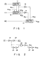
- Fig. 1 is a circuit diagram showing a control circuit corresponding to a section associated with a CS standby mode in a PSRAM of the present embodiment.
- a chip enable control circuit 11 generates a control signal group ( ⁇ CE ⁇ , ⁇ P1, ⁇ P2) in synchronism with a chip enable signal CE ⁇ .
- the chip select control circuit 12 receives the control signal group ( ⁇ CE ⁇ , ⁇ P1, ⁇ P2), latches a chip select signal CS with the use of these control signals, and delivers a latched signal ⁇ CS ⁇ as an output signal.
- a write enable control circuit 13 is responsive to an inverted replica of the latched signal ⁇ CS ⁇ and inverted replica of the control signal coming from the control circuits 12 and 11, respectively, to generate a write enable signal WE ⁇ as an internal write enable signal ⁇ WE, enabling data to be written into a memory cell, not shown. It is to be noted that the latched signals ⁇ CS ⁇ and control signal ⁇ CE ⁇ are supplied as the control signals ⁇ O and ⁇ CE to the write enable control circuit 13 after they have been passed through inverters 14 and 15, respectively.
- Fig. 2 is a circuit diagram showing a practical arrangement of the chip enable control circuit 11 in the present embodiment.
- the chip enable signal CE ⁇ is sequentially inverted through inverters 21 and 22 to provide the aforementioned control signal ⁇ CE ⁇ .
- the output of the inverter 21 is supplied to one input terminal of a NAND gate 25 sequentially through inverters 23 and 24 and directly to the other input terminal of the NAND gate 25.
- the output of the NAND gate 25 is inverted by an inverter 26 to obtain the aforementioned control signal ⁇ P1. Further, the output of the inverter 26 is inverted sequentially through inverters 27 and 28 to obtain the aforementioned control signal ⁇ P2.
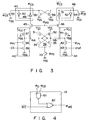
- Fig. 3 is a circuit diagram showing a practical arrangement of a chip select control circuit 12 in Fig. 1.
- the control circuit 12 includes a CMOS type differential amplifier 36 comprised of P channel MOS transistors 31, 32 and N channel MOS transistors 33, 34 and 35.
- the N channel MOS transistor 33 is of such an active type as to make the differential amplifier circuit active.
- the aforementioned control signal ⁇ P2 is supplied to the gate of the MOS transistor 33.
- a chip select signal input section 40 comprises a P channel MOS transistor 37 and N channel MOS transistors 38, 39 and the output of the signal input section 40 is supplied to one input/output node NA of the differential amplifier circuit 36.
- a reference voltage input section 44 comprises a P channel MOS transistor 41 and N channel MOS transistors 42, 43 and the output of the reference voltage input section 44 is supplied to the other input/output node NB.
- the P channel MOS transistors 37 and 41 of the chip select signal input section 40 and reference voltage input section 44, respectively, are used as load transistors and a ground voltage Vss is applied to the gates of the transistors 37 and 41.
- the control signal ⁇ P1 as set out above is supplied to the gates of the N channel MOS transistors 38 and 42 of the chip select signal section and reference voltage input section 44, respectively.
- the chip select signal CS is supplied to the gate of the N channel MOS transistor 39 in the chip select signal input section 40 and a reference voltage Vref is supplied to the gate of the N channel MOS transistor 43 in the reference voltage input section 44, noting that the reference voltage Vref is set to a level intermediate between a high logic level and a low logic level voltage.
- Signals of the paired input/output nodes NA, NB in the differential amplifier circuit 36 are supplied to latch sections 47 and 48 for generating latched signals ⁇ CS, ⁇ CS ⁇ . This is done through N channel MOS transistors 45 and 46 whose gates are supplied with the control signal ⁇ P2 set out above.
- the latches 47 and 48 are of such a type that the latch 47 comprises two inverters 49 and 50 with the output of the inverter 50 connected to the input of the inverter 49 and the latch 48 comprises two inverters 52 and 51 with the output of the inverter 52 connected to the input of the inverter 51.
- a reset N channel MOS transistor 53 is connected across the input terminal of the inverter 50 in the latch section 47 and a ground potential Vss and a reset N channel MOS transistor 54 is connected across the input terminal of the inverter 52 in the latch section and the ground potential Vss.
- the control signal ⁇ CE as set out above is supplied to the gates of these N channel MOS transistors 53 and 54.
- An N channel MOS transistor 55 has its drain-to-source circuit connected across the inverter 49 in the latch circuit 47 and the ground potential Vss and an N channel MOS transistor 56 has its drain-to-source circuit connected across the inverter 51 in the latch section 48 and the ground potential Vss. These transistors 55 and 56 have their gates connected to their corresponding drains.
- Fig. 4 is a detailed arrangement of a write enable control circuit 13 in the embodiment shown in Fig. 2.
- the control circuit 13 comprises a NAND gate 61 supplied with the control signals ⁇ O and ⁇ CE and NOR gate 62 supplied with an output of the NAND gate 61 and write enable signal WE ⁇ .
- the internal write enable signal ⁇ WE ⁇ is obtained as an output of the NOR gate 62.
- the N channel MOS transistor 38 in the chip select signal input section 40 and N channel MOS transistor 42 in the reference voltage input section 44 are turned ON with the "H" level of the control signal ⁇ P1 and a voltage corresponding to the chip select signal CS and reference voltage Vref emerge on the paired input/output nodes NA and NB in the differential amplifier circuit 36.
- the transistor 33 in the differential amplifier circuit 36 is turned ON with the "H" level of the control signal ⁇ P2, placing the differential amplifier circuit 36 in an active state.
- the voltages developed on the chip select signal input section 40 and reference voltage input section 44 compare with each other, detecting a chip select signal CS logic level.
- the N channel MOS transistors 45 and 46 are turned ON and the detection outputs of the differential amplifier circuit 36 are supplied to the latching sections 47 and 48 where they are latched.
- the signal CS becomes a "H” level and the reference voltage Vref is set to an intermediate level of a signal CS logic level.
- the latched signal ⁇ CS of the latch section 47 becomes a "H” level and the latched signal ⁇ CS ⁇ of the latch section 48 becomes a "L" level.
- the NOR gate circuit 62 in the write enable control circuit 13 receives a "L" level write enable signal WE ⁇ , as well as an "L" output signal delivered from the NAND gate circuit 61 which has been supplied with “H” level control signals ⁇ CE and ⁇ O, and delivers a "H” level signal as an internal write enable signal ⁇ WE. That is, a "H" level output control signal ⁇ CE is delivered from the inverter 15 (see Fig. 1) as indicated by an arrow 71 in Fig. 5 and a write enable signal WE ⁇ is reversed at the NOR gate 62 in the write enable control circuit 13. The NOR gate 62 delivers a corresponding "H" level signal as an internal write enable signal ⁇ WE. Thereafter, a write series circuit performs a data write-in control, not shown.
- a chip enable signal CE ⁇ changes to a "H” level standby mode.
- a "H” level control signal ⁇ CE ⁇ is generated from the chip enable control circuit 11 and the transistors 53 and 54 in the chip select control circuit 13 (see Fig. 3) are turned ON.
- the latch sections 47 and 48 are reset and the signals ⁇ CS and ⁇ CS ⁇ are set to "L” levels.
- the control signals ⁇ O and ⁇ CE are supplied to the write enable control circuit 13 as shown in Fig. 1 and become a "H” and a “L” level, respectively.
- An output of the NAND gate circuit 61 in the write enable control circuit 13 becomes a "H” level.
- the internal write enable signal ⁇ WE changes from the "H" level to a "L” level.
- a data write control operation is inhibited in a data write series circuit.
- a chip enable signal CE ⁇ changes from a "H” to a "L” level at which time a CS standby mode is involved with the chip select signal CS at the "L” level.
- the control signal ⁇ CE ⁇ of the chip enable control circuit 11 becomes a "L” level for a predetermined period of time and the control signals ⁇ P1 and ⁇ P2 of the chip enable control circuit 11 becomes a "H” level during a predetermined period of time.
- an inverted replica ⁇ CE of the inverter 15 initially becomes a "H” level as indicated by an arrow 71 in Fig. 5 and the write enable signal WE is inverted in the NOR gate 62 in the write enable control circuit 13 and delivered as a "H" level internal write enable signal ⁇ WE from the write enable control circuit 13. Since, however, the latch signal ⁇ CS of the latch section 47 and latch signal ⁇ CS ⁇ of the latch section 48 become a "L" and "H" level, respectively, with the chip select signal CS at a "L” level, an inverted control signal ⁇ O of the latch signal ⁇ CS ⁇ changes from the "H" level to a "L” level. As a result, the internal write enable signal ⁇ WE rapidly changes to a "L” level as indicated by an arrow 72 in Fig. 5 and a data write control operation is inhibited in the write series circuit, not shown.
- the control signal ⁇ O supplied to the write enable control circuit 13 is normally placed in a high potential level and becomes a low potential level only when the chip select signal CS becomes a low potential level with a fall in the chip enable signal CE ⁇ . It is designed that, when the chip enable signal CE ⁇ goes high, the control signal ⁇ O goes back to a high potential level. By so doing, the operation delay time of the write enable control circuit can be made shorter than in the conventional standby mode, securing no loss of the write operation margin. Since, at a time of the CS standby mode, the write enable signal WE ⁇ is rapidly rendered in an non-active state, it is possible to simultaneously realize a circuit arrangement of less dissipation power.
- a control circuit for controlling an operation mode in a pseudostatic RAM for reducing a dissipation current at the standby time is accomplished without a sacrifice of the write operation margin.
Landscapes
- Engineering & Computer Science (AREA)
- Microelectronics & Electronic Packaging (AREA)
- Computer Hardware Design (AREA)
- Dram (AREA)
- Static Random-Access Memory (AREA)
Applications Claiming Priority (2)
| Application Number | Priority Date | Filing Date | Title |
|---|---|---|---|
| JP130893/90 | 1990-05-21 | ||
| JP2130893A JP2744115B2 (ja) | 1990-05-21 | 1990-05-21 | 疑似スタティックramの制御回路 |
Publications (3)
| Publication Number | Publication Date |
|---|---|
| EP0458213A2 EP0458213A2 (en) | 1991-11-27 |
| EP0458213A3 EP0458213A3 (en) | 1993-01-27 |
| EP0458213B1 true EP0458213B1 (en) | 1996-01-17 |
Family
ID=15045179
Family Applications (1)
| Application Number | Title | Priority Date | Filing Date |
|---|---|---|---|
| EP91108048A Expired - Lifetime EP0458213B1 (en) | 1990-05-21 | 1991-05-17 | Control circuit for controlling an operation mode in a pseudo-static RAM |
Country Status (5)
| Country | Link |
|---|---|
| US (1) | US5301164A (ja) |
| EP (1) | EP0458213B1 (ja) |
| JP (1) | JP2744115B2 (ja) |
| KR (1) | KR950007141B1 (ja) |
| DE (1) | DE69116426T2 (ja) |
Families Citing this family (9)
| Publication number | Priority date | Publication date | Assignee | Title |
|---|---|---|---|---|
| US5617551A (en) * | 1992-09-18 | 1997-04-01 | New Media Corporation | Controller for refreshing a PSRAM using individual automatic refresh cycles |
| US5590088A (en) * | 1993-07-13 | 1996-12-31 | Seiko Epson Corporation | Semiconductor memory device with enable signal conversion circuit operative for reducing current consumption |
| KR0119886B1 (ko) * | 1994-07-27 | 1997-10-17 | 김광호 | 반도체 메모리 장치의 모드설정회로 및 그 방법 |
| US5657293A (en) * | 1995-08-23 | 1997-08-12 | Micron Technology, Inc. | Integrated circuit memory with back end mode disable |
| KR100431303B1 (ko) | 2002-06-28 | 2004-05-12 | 주식회사 하이닉스반도체 | 페이지 기록 모드를 수행할 수 있는 슈도 스태틱램 |
| CN1310299C (zh) * | 2003-05-21 | 2007-04-11 | 中国科学院计算技术研究所 | 基于电路静态时延特性的冒险检测和消除方法 |
| US6985385B2 (en) * | 2003-08-26 | 2006-01-10 | Grandis, Inc. | Magnetic memory element utilizing spin transfer switching and storing multiple bits |
| KR100695512B1 (ko) | 2005-06-30 | 2007-03-15 | 주식회사 하이닉스반도체 | 반도체 메모리 장치 |
| US10332586B1 (en) | 2017-12-19 | 2019-06-25 | Micron Technology, Inc. | Apparatuses and methods for subrow addressing |
Family Cites Families (10)
| Publication number | Priority date | Publication date | Assignee | Title |
|---|---|---|---|---|
| JPS6052513B2 (ja) * | 1981-12-02 | 1985-11-19 | 富士通株式会社 | 半導体記憶装置 |
| US4710903A (en) * | 1986-03-31 | 1987-12-01 | Wang Laboratories, Inc. | Pseudo-static memory subsystem |
| JPH0644393B2 (ja) * | 1986-04-08 | 1994-06-08 | 日本電気株式会社 | 半導体メモリ |
| JPS63166093A (ja) * | 1986-12-26 | 1988-07-09 | Toshiba Corp | 半導体メモリの制御回路 |
| JP2569033B2 (ja) * | 1987-01-16 | 1997-01-08 | 株式会社日立製作所 | 半導体記憶装置 |
| JP2585602B2 (ja) * | 1987-06-10 | 1997-02-26 | 株式会社日立製作所 | 半導体記憶装置 |
| US4879683A (en) * | 1987-09-28 | 1989-11-07 | Texas Instruments Incorporated | A gaas register file having a plurality of latches |
| JPH01194194A (ja) * | 1988-01-29 | 1989-08-04 | Nec Ic Microcomput Syst Ltd | 半導体メモリ装置 |
| JPH01205788A (ja) * | 1988-02-12 | 1989-08-18 | Toshiba Corp | 半導体集積回路 |
| JP2598081B2 (ja) * | 1988-05-16 | 1997-04-09 | 株式会社東芝 | 半導体メモリ |
-
1990
- 1990-05-21 JP JP2130893A patent/JP2744115B2/ja not_active Expired - Lifetime
-
1991
- 1991-05-17 DE DE69116426T patent/DE69116426T2/de not_active Expired - Lifetime
- 1991-05-17 KR KR1019910008047A patent/KR950007141B1/ko not_active IP Right Cessation
- 1991-05-17 EP EP91108048A patent/EP0458213B1/en not_active Expired - Lifetime
- 1991-05-20 US US07/702,375 patent/US5301164A/en not_active Expired - Lifetime
Also Published As
| Publication number | Publication date |
|---|---|
| DE69116426D1 (de) | 1996-02-29 |
| KR950007141B1 (ko) | 1995-06-30 |
| JPH0426986A (ja) | 1992-01-30 |
| KR910020732A (ko) | 1991-12-20 |
| US5301164A (en) | 1994-04-05 |
| JP2744115B2 (ja) | 1998-04-28 |
| EP0458213A2 (en) | 1991-11-27 |
| EP0458213A3 (en) | 1993-01-27 |
| DE69116426T2 (de) | 1996-06-05 |
Similar Documents
| Publication | Publication Date | Title |
|---|---|---|
| EP0017990B1 (en) | Integrated memory circuit | |
| US4417328A (en) | Random access semiconductor memory device using MOS transistors | |
| US4161040A (en) | Data-in amplifier for an MISFET memory device having a clamped output except during the write operation | |
| US5243573A (en) | Sense amplifier for nonvolatile semiconductor storage devices | |
| US20050243629A1 (en) | Apparatus for controlling self-refresh period in memory device | |
| US4661928A (en) | Output buffer in which inductive noise is suppressed | |
| US4876669A (en) | MOS static type RAM having a variable load | |
| US4558241A (en) | Sense amplifier | |
| US5539691A (en) | Semiconductor memory device and method for reading and writing data therein | |
| US4104733A (en) | Address selecting circuitry for semiconductor memory device | |
| EP0176203A2 (en) | Self refresh control circuit for dynamic semiconductor memory device | |
| EP0096421B1 (en) | Static memory device with signal transition detector | |
| US4733112A (en) | Sense amplifier for a semiconductor memory device | |
| US3938109A (en) | High speed ECL compatible MOS-Ram | |
| US6255862B1 (en) | Latch type sense amplifier circuit | |
| EP0458213B1 (en) | Control circuit for controlling an operation mode in a pseudo-static RAM | |
| US3946369A (en) | High speed MOS RAM employing depletion loads | |
| US5148399A (en) | Sense amplifier circuitry selectively separable from bit lines for dynamic random access memory | |
| US5208773A (en) | Semiconductor memory device having bit lines and word lines different in data reading and data writing | |
| US6292418B1 (en) | Semiconductor memory device | |
| KR910004733B1 (ko) | 데이타 버스 리셋트 회로를 지닌 반도체 기억장치 | |
| US5815450A (en) | Semiconductor memory device | |
| US5608677A (en) | Boosting voltage circuit used in active cycle of a semiconductor memory device | |
| US4823322A (en) | Dynamic random access memory device having an improved timing arrangement | |
| US4554469A (en) | Static bootstrap semiconductor drive circuit |
Legal Events
| Date | Code | Title | Description |
|---|---|---|---|
| PUAI | Public reference made under article 153(3) epc to a published international application that has entered the european phase |
Free format text: ORIGINAL CODE: 0009012 |
|
| 17P | Request for examination filed |
Effective date: 19910517 |
|
| AK | Designated contracting states |
Kind code of ref document: A2 Designated state(s): DE FR GB |
|
| PUAL | Search report despatched |
Free format text: ORIGINAL CODE: 0009013 |
|
| AK | Designated contracting states |
Kind code of ref document: A3 Designated state(s): DE FR GB |
|
| 17Q | First examination report despatched |
Effective date: 19950407 |
|
| GRAA | (expected) grant |
Free format text: ORIGINAL CODE: 0009210 |
|
| AK | Designated contracting states |
Kind code of ref document: B1 Designated state(s): DE FR GB |
|
| REF | Corresponds to: |
Ref document number: 69116426 Country of ref document: DE Date of ref document: 19960229 |
|
| ET | Fr: translation filed | ||
| PLBE | No opposition filed within time limit |
Free format text: ORIGINAL CODE: 0009261 |
|
| STAA | Information on the status of an ep patent application or granted ep patent |
Free format text: STATUS: NO OPPOSITION FILED WITHIN TIME LIMIT |
|
| 26N | No opposition filed | ||
| REG | Reference to a national code |
Ref country code: GB Ref legal event code: 746 Effective date: 19981012 |
|
| REG | Reference to a national code |
Ref country code: FR Ref legal event code: D6 |
|
| REG | Reference to a national code |
Ref country code: GB Ref legal event code: IF02 |
|
| REG | Reference to a national code |
Ref country code: FR Ref legal event code: ST Effective date: 20090119 |
|
| REG | Reference to a national code |
Ref country code: FR Ref legal event code: D3 |
|
| PGFP | Annual fee paid to national office [announced via postgrant information from national office to epo] |
Ref country code: GB Payment date: 20100329 Year of fee payment: 20 |
|
| PGFP | Annual fee paid to national office [announced via postgrant information from national office to epo] |
Ref country code: FR Payment date: 20100525 Year of fee payment: 20 |
|
| PGFP | Annual fee paid to national office [announced via postgrant information from national office to epo] |
Ref country code: DE Payment date: 20100512 Year of fee payment: 20 |
|
| REG | Reference to a national code |
Ref country code: DE Ref legal event code: R071 Ref document number: 69116426 Country of ref document: DE |
|
| REG | Reference to a national code |
Ref country code: GB Ref legal event code: PE20 Expiry date: 20110516 |
|
| PG25 | Lapsed in a contracting state [announced via postgrant information from national office to epo] |
Ref country code: GB Free format text: LAPSE BECAUSE OF EXPIRATION OF PROTECTION Effective date: 20110516 |
|
| PG25 | Lapsed in a contracting state [announced via postgrant information from national office to epo] |
Ref country code: DE Free format text: LAPSE BECAUSE OF EXPIRATION OF PROTECTION Effective date: 20110517 |