EP0455032A2 - Process for forming multi-level coplanar conductor/insulator films employing photosensitive polyimide polymer compositions - Google Patents
Process for forming multi-level coplanar conductor/insulator films employing photosensitive polyimide polymer compositions Download PDFInfo
- Publication number
- EP0455032A2 EP0455032A2 EP91105941A EP91105941A EP0455032A2 EP 0455032 A2 EP0455032 A2 EP 0455032A2 EP 91105941 A EP91105941 A EP 91105941A EP 91105941 A EP91105941 A EP 91105941A EP 0455032 A2 EP0455032 A2 EP 0455032A2
- Authority
- EP
- European Patent Office
- Prior art keywords
- layer
- conductor
- photosensitive polyimide
- insulator
- polyimide polymer
- Prior art date
- Legal status (The legal status is an assumption and is not a legal conclusion. Google has not performed a legal analysis and makes no representation as to the accuracy of the status listed.)
- Granted
Links
Images
Classifications
-
- H—ELECTRICITY
- H10—SEMICONDUCTOR DEVICES; ELECTRIC SOLID-STATE DEVICES NOT OTHERWISE PROVIDED FOR
- H10W—GENERIC PACKAGES, INTERCONNECTIONS, CONNECTORS OR OTHER CONSTRUCTIONAL DETAILS OF DEVICES COVERED BY CLASS H10
- H10W20/00—Interconnections in chips, wafers or substrates
- H10W20/01—Manufacture or treatment
- H10W20/071—Manufacture or treatment of dielectric parts thereof
- H10W20/093—Manufacture or treatment of dielectric parts thereof by modifying materials of the dielectric parts
- H10W20/097—Manufacture or treatment of dielectric parts thereof by modifying materials of the dielectric parts by thermally treating
-
- H—ELECTRICITY
- H05—ELECTRIC TECHNIQUES NOT OTHERWISE PROVIDED FOR
- H05K—PRINTED CIRCUITS; CASINGS OR CONSTRUCTIONAL DETAILS OF ELECTRIC APPARATUS; MANUFACTURE OF ASSEMBLAGES OF ELECTRICAL COMPONENTS
- H05K3/00—Apparatus or processes for manufacturing printed circuits
- H05K3/0011—Working of insulating substrates or insulating layers
- H05K3/0017—Etching of the substrate by chemical or physical means
- H05K3/0023—Etching of the substrate by chemical or physical means by exposure and development of a photosensitive insulating layer
-
- H—ELECTRICITY
- H05—ELECTRIC TECHNIQUES NOT OTHERWISE PROVIDED FOR
- H05K—PRINTED CIRCUITS; CASINGS OR CONSTRUCTIONAL DETAILS OF ELECTRIC APPARATUS; MANUFACTURE OF ASSEMBLAGES OF ELECTRICAL COMPONENTS
- H05K3/00—Apparatus or processes for manufacturing printed circuits
- H05K3/46—Manufacturing multilayer circuits
- H05K3/4644—Manufacturing multilayer circuits by building the multilayer layer by layer, i.e. build-up multilayer circuits
- H05K3/467—Adding a circuit layer by thin film methods
-
- H—ELECTRICITY
- H10—SEMICONDUCTOR DEVICES; ELECTRIC SOLID-STATE DEVICES NOT OTHERWISE PROVIDED FOR
- H10W—GENERIC PACKAGES, INTERCONNECTIONS, CONNECTORS OR OTHER CONSTRUCTIONAL DETAILS OF DEVICES COVERED BY CLASS H10
- H10W20/00—Interconnections in chips, wafers or substrates
- H10W20/01—Manufacture or treatment
- H10W20/071—Manufacture or treatment of dielectric parts thereof
- H10W20/081—Manufacture or treatment of dielectric parts thereof by forming openings in the dielectric parts
- H10W20/084—Manufacture or treatment of dielectric parts thereof by forming openings in the dielectric parts for dual-damascene structures
-
- H—ELECTRICITY
- H10—SEMICONDUCTOR DEVICES; ELECTRIC SOLID-STATE DEVICES NOT OTHERWISE PROVIDED FOR
- H10W—GENERIC PACKAGES, INTERCONNECTIONS, CONNECTORS OR OTHER CONSTRUCTIONAL DETAILS OF DEVICES COVERED BY CLASS H10
- H10W20/00—Interconnections in chips, wafers or substrates
- H10W20/01—Manufacture or treatment
- H10W20/071—Manufacture or treatment of dielectric parts thereof
- H10W20/093—Manufacture or treatment of dielectric parts thereof by modifying materials of the dielectric parts
- H10W20/095—Manufacture or treatment of dielectric parts thereof by modifying materials of the dielectric parts by irradiating with electromagnetic or particle radiation
-
- H—ELECTRICITY
- H10—SEMICONDUCTOR DEVICES; ELECTRIC SOLID-STATE DEVICES NOT OTHERWISE PROVIDED FOR
- H10W—GENERIC PACKAGES, INTERCONNECTIONS, CONNECTORS OR OTHER CONSTRUCTIONAL DETAILS OF DEVICES COVERED BY CLASS H10
- H10W20/00—Interconnections in chips, wafers or substrates
- H10W20/40—Interconnections external to wafers or substrates, e.g. back-end-of-line [BEOL] metallisations or vias connecting to gate electrodes
- H10W20/41—Interconnections external to wafers or substrates, e.g. back-end-of-line [BEOL] metallisations or vias connecting to gate electrodes characterised by their conductive parts
- H10W20/42—Vias, e.g. via plugs
-
- H—ELECTRICITY
- H05—ELECTRIC TECHNIQUES NOT OTHERWISE PROVIDED FOR
- H05K—PRINTED CIRCUITS; CASINGS OR CONSTRUCTIONAL DETAILS OF ELECTRIC APPARATUS; MANUFACTURE OF ASSEMBLAGES OF ELECTRICAL COMPONENTS
- H05K2201/00—Indexing scheme relating to printed circuits covered by H05K1/00
- H05K2201/01—Dielectrics
- H05K2201/0137—Materials
- H05K2201/0154—Polyimide
-
- H—ELECTRICITY
- H05—ELECTRIC TECHNIQUES NOT OTHERWISE PROVIDED FOR
- H05K—PRINTED CIRCUITS; CASINGS OR CONSTRUCTIONAL DETAILS OF ELECTRIC APPARATUS; MANUFACTURE OF ASSEMBLAGES OF ELECTRICAL COMPONENTS
- H05K3/00—Apparatus or processes for manufacturing printed circuits
- H05K3/02—Apparatus or processes for manufacturing printed circuits in which the conductive material is applied to the surface of the insulating support and is thereafter removed from such areas of the surface which are not intended for current conducting or shielding
- H05K3/04—Apparatus or processes for manufacturing printed circuits in which the conductive material is applied to the surface of the insulating support and is thereafter removed from such areas of the surface which are not intended for current conducting or shielding the conductive material being removed mechanically, e.g. by punching
- H05K3/045—Apparatus or processes for manufacturing printed circuits in which the conductive material is applied to the surface of the insulating support and is thereafter removed from such areas of the surface which are not intended for current conducting or shielding the conductive material being removed mechanically, e.g. by punching by making a conductive layer having a relief pattern, followed by abrading of the raised portions
-
- H—ELECTRICITY
- H05—ELECTRIC TECHNIQUES NOT OTHERWISE PROVIDED FOR
- H05K—PRINTED CIRCUITS; CASINGS OR CONSTRUCTIONAL DETAILS OF ELECTRIC APPARATUS; MANUFACTURE OF ASSEMBLAGES OF ELECTRICAL COMPONENTS
- H05K3/00—Apparatus or processes for manufacturing printed circuits
- H05K3/10—Apparatus or processes for manufacturing printed circuits in which conductive material is applied to the insulating support in such a manner as to form the desired conductive pattern
- H05K3/107—Apparatus or processes for manufacturing printed circuits in which conductive material is applied to the insulating support in such a manner as to form the desired conductive pattern by filling grooves in the support with conductive material
-
- H—ELECTRICITY
- H05—ELECTRIC TECHNIQUES NOT OTHERWISE PROVIDED FOR
- H05K—PRINTED CIRCUITS; CASINGS OR CONSTRUCTIONAL DETAILS OF ELECTRIC APPARATUS; MANUFACTURE OF ASSEMBLAGES OF ELECTRICAL COMPONENTS
- H05K3/00—Apparatus or processes for manufacturing printed circuits
- H05K3/46—Manufacturing multilayer circuits
- H05K3/4644—Manufacturing multilayer circuits by building the multilayer layer by layer, i.e. build-up multilayer circuits
- H05K3/465—Manufacturing multilayer circuits by building the multilayer layer by layer, i.e. build-up multilayer circuits by applying an insulating layer having channels for the next circuit layer
Definitions
- This invention relates to the manufacture of VLSI semiconductor chips, boards and assemblies, and, more particularly, to a process for forming multi-level coplanar metal insulator films on a substrate.
- multi-level metal patterns are used to interconnect devices.
- One technique for accomplishing this is disclosed in IBM Tech. Discl. Bull., Vol. 25, No. 10 (Mar. 1983), pp. 5309-5314, where a first metal pattern is formed in an insulator layer. An insulator layer is deposited, and a series of holes are etched through this layer in locations where interconnections (or stud vias) are desired. The holes are filled with metal, excess metal is lifted off, and another insulator layer is deposited; this layer is patterned, and metal is deposited in these openings, thus making contact with the first metal pattern. This process is cumbersome and costly to carry out, however, as it involves several sequences of masking and etching steps.
- a less cumbersome process which employs at least two insulator layers comprising a photosensitive polyimide polymer composition. Openings are formed directly in the insulator layers, without requiring the use of masking layers and pattern transfer steps. The openings which are in at least partial alignment are simultaneously filled with a conductor material, and the material which overlies the upper insulator layer is removed to achieve a coplanar conductor/insulator film. The process steps can be repeated to form additional coplanar conductor/insulator films.
- the process involves forming multi-level coplanar conductor/insulator films on a substrate having a conductor pattern, by first applying a first layer comprising a photosensitive polyimide polymer composition to the substrate, and exposing the first layer to a pattern of ultraviolet radiation.
- a second layer comprising a photosensitive polyimide polymer composition is applied to the first layer, and the second layer is exposed to a pattern of ultraviolet radiation.
- the first and second layers are developed so as to selectively expose regions of the substrate, the openings in the first layer being in alignment with at least a portion of the openings formed in the second layer.
- a conductor material is deposited on the second layer and in the openings in the first and second layers, and then the conductor material which overlies the second layer is removed to coplanarize the surfaces of conductor material and the second layer.
- the process starts by applying a first insulator layer 1 to a processed semiconductor substrate, indicated generally by the numeral 2.
- the substrate 2 comprises a planarized insulator layer 3 which includes a pattern of conductor material 4.
- the insulator layer 3 is disposed over an integrated circuit chip, and the conductor material 4 is contact metallurgy to devices (not shown) formed in the chip.
- the first insulator layer 1 is deposited over the substrate 2 by spin application, at about 2000 - 6000 rpm for about 20 - 60 seconds, and then baked at a temperature of about 70 - 90°C for about 10 - 30 minutes.
- the planarized insulator layer 3 commonly comprises silicon dioxide or reflowed phosphosilicate glass, and the conductor material 4 may be, for example, copper-doped aluminum or doped polycrystalline silicon.
- both the first insulator layer 1, as well as a second insulator layer 6, to be described below, comprise a photosensitive polyimide polymer composition.
- a desired pattern of openings can be formed directly in each of the layers 1 and 6, without requiring application of separate masking layers, followed by image transfer steps.
- Suitable photosensitive polyimide polymer compositions are disclosed, for example, in U.S. Pat. No. 4,629,777, issued to Pfeifer on Dec. 16, 1986; U.S. Pat No. 4,657,832, issued to Pfeifer on Apr. 14, 1987; U.S. Pat. No. 4,698,295, issued to Pfeifer, et al. on Oct. 6, 1987; and U.S.
- the polymer composition comprises a fully imidized solvent soluble polyimide with a structural unit having the general formula where R represents an aliphatic group, such as methyl, and R' represents an optional aliphatic substituent which may be the same as or different from R, and a suitable solvent for the polymer.
- the insulator layer 1 is then exposed in a predetermined pattern to radiation, such as UV light, in a conventional manner.
- the region, designated as 5, represents that portion of the first insulator layer 1, which has not been exposed.
- a second insulator layer 6 is applied to the first insulator layer 1, prior to development. Then, the second insulator layer 6 is exposed in a predetermined pattern to radiation, as described above, with the region, designated as 7 in Fig. 4, representing that portion of the second insulator layer 6, which has not been exposed.
- the method of applying and exposing the second insulator layer 6, as well as the composition are as described above.
- the first insulator layer 1 is applied to a thickness typically ranging from about 0.2 - 1 microns, preferably from about 0.6 - 0.7 microns, while the second insulator layer 6 has a thickness usually ranging from about 0.05 - 1.2 microns, preferably from about 0.2 - 0.5 microns.
- the unexposed regions 5 and 7 of the insulator layers 1 and 6, respectively, are simultaneously removed to selectively expose regions of the substrate 2.
- the unexposed regions 5 and 7 are removed, preferably by spraying with a conventional developer, such as, for example, gammabutylactone.
- a conventional developer such as, for example, gammabutylactone.
- the development time will depend on the thicknesses of the first and second insulator layers 1 and 6, as well as other factors known to those skilled in the art. This provides the structure shown in Fig. 5.
- the openings formed in the first insulator layer 1 are in at least partial alignment with those formed in the second insulator layer 6.
- the openings in the first insulator layer 1 allow contact to be made to the pattern 4 in the substrate 2.
- the structure, as shown in Fig. 5, allows simultaneous formation of conductor material in the openings in the second insulator layer 6 (i.e., wiring channels) and in the openings in the first insulator layer 1 (i.e., stud vias).
- the structure is then subjected to a heating step so as to cure the polyimide layers 1 and 6.
- this step is carried out at a temperature of at least about 10°C above the temperature at which the conductor material 8 is to be applied, as discussed below.
- this temperature is at least about 350°C, and is usually within the range of about 350°-450°C, depending upon the conductor material 10 which is employed.
- the openings in the layers 1 and 6 are overfilled with conductor material 8, preferably metal, for example, aluminum, copper, Al-Cu, Al-Si or tungsten, preferably by physical vapor deposition, such as evaporation or sputtering, chemical vapor deposition or by plating.
- conductor material 8 preferably metal, for example, aluminum, copper, Al-Cu, Al-Si or tungsten, preferably by physical vapor deposition, such as evaporation or sputtering, chemical vapor deposition or by plating.
- the thickness of the conductor material 8 is at least as great as the combined thicknesses of the insulator layers 1 and 6.
- the conductor material 8, which overlies the second insulating layer 6 is removed so as to coplanarize the surfaces of the conductor material 8 and the second insulator layer 6.
- a preferred method to accomplish this is by using chemical-mechanical polishing, as taught, for example, in Eur. Pat. Appln., No. 0,223,920, published Jun. 3, 1987, by Beyer, et al., the entire disclosure of which is incorporated herein by reference. That process involves the concurrent chemical and mechanical polishing of an overlying layer to expose the surface of a non-planar underlying layer on which it is formed, one layer of which is a conductive film, and the other, an insulator film.
- the process removes the overlying layer at a faster rate than the underlying layer, until the upper surface of the overlying layer becomes coplanar with that of the underlying layer.
- coplanarization can be accomplished by standard sacrificial planarization methods, such as etchback, as should be apparent to those skilled in the art.
- conductor layer 8 is the final metal level of the semiconductor structure, final passivation insulator is applied over the substrate. Otherwise, if additional levels of metallization are to be formed, then the steps as described above are repeated for each level desired.
- a sample process flow for this embodiment, prior to application and planarization of metal, is as follows: Spin apply 0.1% 3-aminopropyltriethoxysilane (commercially available from Union Carbide under the designation "A1100") in methanol to a processed semiconductor substrate containing a pattern of metallization; Spin apply "PROBIMIDE 408" at 500 rpms, then hold at 4,000 rpms for 25 sec.; Bake at 80°C for 20 min.; Expose to UV light (270 mj at 365 nm); Spin apply "PROBIMIDE 408” and bake as above; Expose to UV light (270 mj at 365 nm); Simultaneously develop first and second "PROBIMIDE 408" layers with a 45 sec. spray of gammabutylactone at 500 rpms; Rinse with a 20 sec. spray of xylene at 500 rpms; Dry with N2; and Ramp cure to 350°C.
- the present invention provides multi-level coplanar conductor/insulator films, by forming the desired channels and stud vias directly in the insulator layers, without the need for separate masking layers and image transfer steps. Accordingly, the need for resist stripping operations, which can damage the patterns formed in the insulator layers, is also avoided.
Landscapes
- Engineering & Computer Science (AREA)
- Manufacturing & Machinery (AREA)
- Microelectronics & Electronic Packaging (AREA)
- Internal Circuitry In Semiconductor Integrated Circuit Devices (AREA)
- Macromolecular Compounds Obtained By Forming Nitrogen-Containing Linkages In General (AREA)
- Formation Of Insulating Films (AREA)
Abstract
Description
- This invention relates to the manufacture of VLSI semiconductor chips, boards and assemblies, and, more particularly, to a process for forming multi-level coplanar metal insulator films on a substrate.
- In the field of VLSI semiconductor chip processing, multi-level metal patterns are used to interconnect devices. One technique for accomplishing this is disclosed in IBM Tech. Discl. Bull., Vol. 25, No. 10 (Mar. 1983), pp. 5309-5314, where a first metal pattern is formed in an insulator layer. An insulator layer is deposited, and a series of holes are etched through this layer in locations where interconnections (or stud vias) are desired. The holes are filled with metal, excess metal is lifted off, and another insulator layer is deposited; this layer is patterned, and metal is deposited in these openings, thus making contact with the first metal pattern. This process is cumbersome and costly to carry out, however, as it involves several sequences of masking and etching steps.
- A simpler approach is shown in U.S. Pat. No. 4,789,648, issued to Chow, et al. on Dec. 6, 1988, which includes the following steps: depositing an insulator layer over an underlying insulator layer containing a metal pattern; applying an etch stop layer; defining holes in the etch stop; depositing another insulator layer; etching openings (or wiring channels) in the upper insulator layer in alignment with the holes in the etch stop, and continuing the etching into the first insulator layer to form via holes; overfilling the channels and via holes with metal; and then removing the excess metal to form a coplanar metal/insulator surface. While this process is less complicated than that disclosed in the article discussed above, nevertheless, it still involves two sequences of masking and etching steps to form the via holes and the wiring channels.
- Another conventional technique, known as the pillar process, is exemplified in U.S. Pat. No. 4,621,045, issued to Goodner on Nov. 4, 1986, in which a conductive pillar is provided in an insulator layer to connect two layers of metal. This process also has a high degree of complexity, however, with multiple masking and etching sequences.
- Now, in accordance with the present invention as claimed, there is provided a less cumbersome process, which employs at least two insulator layers comprising a photosensitive polyimide polymer composition. Openings are formed directly in the insulator layers, without requiring the use of masking layers and pattern transfer steps. The openings which are in at least partial alignment are simultaneously filled with a conductor material, and the material which overlies the upper insulator layer is removed to achieve a coplanar conductor/insulator film. The process steps can be repeated to form additional coplanar conductor/insulator films.
- In a preferred embodiment, the process involves forming multi-level coplanar conductor/insulator films on a substrate having a conductor pattern, by first applying a first layer comprising a photosensitive polyimide polymer composition to the substrate, and exposing the first layer to a pattern of ultraviolet radiation. A second layer comprising a photosensitive polyimide polymer composition is applied to the first layer, and the second layer is exposed to a pattern of ultraviolet radiation. The first and second layers are developed so as to selectively expose regions of the substrate, the openings in the first layer being in alignment with at least a portion of the openings formed in the second layer. A conductor material is deposited on the second layer and in the openings in the first and second layers, and then the conductor material which overlies the second layer is removed to coplanarize the surfaces of conductor material and the second layer.
- The foregoing and other objects, features and advantages of the invention will be apparent from the following more particular description of the preferred embodiments of the invention.
- Figs. 1-7
- are cross-sectional views of a semiconductor structure illustrating the structure that results at various stages of the process of a preferred embodiment of the invention.
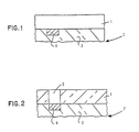
- Referring to Fig. 1, the process starts by applying a
first insulator layer 1 to a processed semiconductor substrate, indicated generally by thenumeral 2. Typically, thesubstrate 2 comprises aplanarized insulator layer 3 which includes a pattern ofconductor material 4. In general, theinsulator layer 3 is disposed over an integrated circuit chip, and theconductor material 4 is contact metallurgy to devices (not shown) formed in the chip. Preferably, thefirst insulator layer 1 is deposited over thesubstrate 2 by spin application, at about 2000 - 6000 rpm for about 20 - 60 seconds, and then baked at a temperature of about 70 - 90°C for about 10 - 30 minutes. It should be noted that it is also preferred, to improve adhesion, to apply a conventional adhesion promoter, such as 0.1% 3-aminopropyltriethoxysilane (commercially available from Union Carbide under the designation "A1100") in methanol, to the substrate before depositing thefirst insulator layer 1. In general, theplanarized insulator layer 3 commonly comprises silicon dioxide or reflowed phosphosilicate glass, and theconductor material 4 may be, for example, copper-doped aluminum or doped polycrystalline silicon. - It is an important feature of the invention, that both the
first insulator layer 1, as well as asecond insulator layer 6, to be described below, comprise a photosensitive polyimide polymer composition. Thus, a desired pattern of openings can be formed directly in each of thelayers 
where R represents an aliphatic group, such as methyl, and R' represents an optional aliphatic substituent which may be the same as or different from R, and a suitable solvent for the polymer. (The R' substituent can enhance the photospeed or increase the Tg-value of the polymer.) Such photosensitive polyimide polymer compositions are disclosed in Pfeifer, et al., "Direct Photoimaging of Fully Imidized Solvent-Soluble Polyimides", Second International Conference on Polyimides, Mid-Hudson Section SPE, Ellenville, N.Y. (Oct. 30-Nov. 1, 1985), the entire disclosure of which is incorporated herein by reference. In a particularly preferred embodiment, the "PROBIMIDE 400" series, preferably "PROBIMIDE 408", commercially available from Ciba-Geigy Corp., is employed. - As shown in Fig 2, the
insulator layer 1 is then exposed in a predetermined pattern to radiation, such as UV light, in a conventional manner. The region, designated as 5, represents that portion of thefirst insulator layer 1, which has not been exposed. - Referring to Fig. 3, a
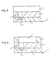
second insulator layer 6 is applied to thefirst insulator layer 1, prior to development. Then, thesecond insulator layer 6 is exposed in a predetermined pattern to radiation, as described above, with the region, designated as 7 in Fig. 4, representing that portion of thesecond insulator layer 6, which has not been exposed. Again, in general, the method of applying and exposing thesecond insulator layer 6, as well as the composition, are as described above. - It should be noted that in general, the
first insulator layer 1 is applied to a thickness typically ranging from about 0.2 - 1 microns, preferably from about 0.6 - 0.7 microns, while thesecond insulator layer 6 has a thickness usually ranging from about 0.05 - 1.2 microns, preferably from about 0.2 - 0.5 microns. - Next, the
unexposed regions insulator layers substrate 2. For example, when "PROBIMIDE 408" is used as the photosensitive polyimide polymer composition, theunexposed regions second insulator layers - Referring again to Fig. 5, the openings formed in the
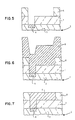
first insulator layer 1 are in at least partial alignment with those formed in thesecond insulator layer 6. The openings in thefirst insulator layer 1 allow contact to be made to thepattern 4 in thesubstrate 2. The structure, as shown in Fig. 5, allows simultaneous formation of conductor material in the openings in the second insulator layer 6 (i.e., wiring channels) and in the openings in the first insulator layer 1 (i.e., stud vias). - The structure, as shown in Fig. 5, is then subjected to a heating step so as to cure the
polyimide layers conductor material 8 is to be applied, as discussed below. Typically, this temperature is at least about 350°C, and is usually within the range of about 350°-450°C, depending upon the conductor material 10 which is employed. - Next, as shown in Fig. 6, the openings in the
layers conductor material 8, preferably metal, for example, aluminum, copper, Al-Cu, Al-Si or tungsten, preferably by physical vapor deposition, such as evaporation or sputtering, chemical vapor deposition or by plating. It should be noted that the thickness of theconductor material 8 is at least as great as the combined thicknesses of theinsulator layers - In the next step, as shown in Fig. 7, the
conductor material 8, which overlies the secondinsulating layer 6 is removed so as to coplanarize the surfaces of theconductor material 8 and thesecond insulator layer 6. A preferred method to accomplish this is by using chemical-mechanical polishing, as taught, for example, in Eur. Pat. Appln., No. 0,223,920, published Jun. 3, 1987, by Beyer, et al., the entire disclosure of which is incorporated herein by reference. That process involves the concurrent chemical and mechanical polishing of an overlying layer to expose the surface of a non-planar underlying layer on which it is formed, one layer of which is a conductive film, and the other, an insulator film. Using a polishing pad and a slurry, the process removes the overlying layer at a faster rate than the underlying layer, until the upper surface of the overlying layer becomes coplanar with that of the underlying layer. As another alternative, coplanarization can be accomplished by standard sacrificial planarization methods, such as etchback, as should be apparent to those skilled in the art. - If the
conductor layer 8 is the final metal level of the semiconductor structure, final passivation insulator is applied over the substrate. Otherwise, if additional levels of metallization are to be formed, then the steps as described above are repeated for each level desired. - Various modifications can be made in the process, as will be apparent to those skilled in the art.
- A sample process flow for this embodiment, prior to application and planarization of metal, is as follows:
Spin apply 0.1% 3-aminopropyltriethoxysilane (commercially available from Union Carbide under the designation "A1100") in methanol to a processed semiconductor substrate containing a pattern of metallization;
Spin apply "PROBIMIDE 408" at 500 rpms, then hold at 4,000 rpms for 25 sec.; Bake at 80°C for 20 min.;
Expose to UV light (270 mj at 365 nm);
Spin apply "PROBIMIDE 408" and bake as above;
Expose to UV light (270 mj at 365 nm);
Simultaneously develop first and second "PROBIMIDE 408" layers with a 45 sec. spray of gammabutylactone at 500 rpms;
Rinse with a 20 sec. spray of xylene at 500 rpms;
Dry with N₂; and
Ramp cure to 350°C. - As such, the present invention provides multi-level coplanar conductor/insulator films, by forming the desired channels and stud vias directly in the insulator layers, without the need for separate masking layers and image transfer steps. Accordingly, the need for resist stripping operations, which can damage the patterns formed in the insulator layers, is also avoided.
Claims (7)
- A process for forming multi-level coplanar conductor/insulator films on a substrate (2) having a conductor pattern (4), comprising the steps of:
applying a first layer (1) comprising a photosensitive polyimide polymer composition to said substrate;
exposing said first layer to a pattern of ultraviolet radiation;
applying a second layer (6) comprising a photosensitive polyimide polymer composition to said first layer;
exposing said second layer to a pattern of ultraviolet radiation;
developing said first and second layers so as to selectively expose regions of said substrate, the openings (5) in said first layer being in alignment with at least a portion of the openings (7) formed in said second layer;
depositing a conductor material (8) on said second layer and in said openings in said first and second layers; and
removing said conductor material which overlies said second layer to coplanarize the surfaces of conductor material and said second layer. - The process of Claim 1, wherein said steps are repeated to form additional coplanar conductor/insulator films.
- The process of Claim 1 or 2, wherein said photosensitive polyimide polymer composition comprises a fully imidized solvent soluble polyimide with a structural unit having the general formula

- The process of Claim 1, 2 or 3, wherein said conductor material is a metal selected from aluminum, copper, Al-Cu, Al-Si and tungsten.
- The process of any one of the preceding claims, wherein said first layer has a thickness ranging from about 0.2 to about 1 microns, preferably from 0,6 to 0,7 microns; and said second layer has a thickness ranging from about 0.05 to about 1.2 microns, preferably from 0,2 to 0,5 microns.
- The process of any one of the preceding claims, wherein said conductor material which overlies said second layer is removed by using chemical-mechanical polishing.
- A semiconductor structure manufactured according to the process of any one of the preceding claims.
Applications Claiming Priority (2)
| Application Number | Priority Date | Filing Date | Title |
|---|---|---|---|
| US07/516,415 US5229257A (en) | 1990-04-30 | 1990-04-30 | Process for forming multi-level coplanar conductor/insulator films employing photosensitive polymide polymer compositions |
| US516415 | 1990-04-30 |
Publications (3)
| Publication Number | Publication Date |
|---|---|
| EP0455032A2 true EP0455032A2 (en) | 1991-11-06 |
| EP0455032A3 EP0455032A3 (en) | 1992-04-15 |
| EP0455032B1 EP0455032B1 (en) | 1995-11-08 |
Family
ID=24055475
Family Applications (1)
| Application Number | Title | Priority Date | Filing Date |
|---|---|---|---|
| EP91105941A Expired - Lifetime EP0455032B1 (en) | 1990-04-30 | 1991-04-13 | Process for forming multi-level coplanar conductor/insulator films employing photosensitive polyimide polymer compositions |
Country Status (4)
| Country | Link |
|---|---|
| US (1) | US5229257A (en) |
| EP (1) | EP0455032B1 (en) |
| JP (1) | JPH0831522B2 (en) |
| DE (1) | DE69114346T2 (en) |
Cited By (3)
| Publication number | Priority date | Publication date | Assignee | Title |
|---|---|---|---|---|
| DE19525745A1 (en) * | 1994-07-14 | 1996-01-18 | Hyundai Electronics Ind | Process for forming a coverage pattern |
| DE19614164A1 (en) * | 1995-10-19 | 1997-04-24 | Mitsubishi Electric Corp | Laminated connection on semiconductor substrate formation method for DRAM |
| US6080832A (en) * | 1998-09-10 | 2000-06-27 | Industrial Technology Research Institute | Low-pretilt alignment layer material |
Families Citing this family (16)
| Publication number | Priority date | Publication date | Assignee | Title |
|---|---|---|---|---|
| US5627345A (en) * | 1991-10-24 | 1997-05-06 | Kawasaki Steel Corporation | Multilevel interconnect structure |
| US5503961A (en) * | 1994-11-02 | 1996-04-02 | International Business Machines Corporation | Process for forming multilayer lift-off structures |
| JP2845176B2 (en) * | 1995-08-10 | 1999-01-13 | 日本電気株式会社 | Semiconductor device |
| US5722162A (en) * | 1995-10-12 | 1998-03-03 | Fujitsu Limited | Fabrication procedure for a stable post |
| KR100206597B1 (en) * | 1995-12-29 | 1999-07-01 | 김영환 | Manufacturing method of fine pattern of semiconductor device |
| US5818110A (en) * | 1996-11-22 | 1998-10-06 | International Business Machines Corporation | Integrated circuit chip wiring structure with crossover capability and method of manufacturing the same |
| US6576848B1 (en) | 1996-11-22 | 2003-06-10 | International Business Machines Corporation | Integrated circuit chip wiring structure with crossover capability and method of manufacturing the same |
| US5856068A (en) * | 1997-05-02 | 1999-01-05 | Motorola, Inc. | Method for fabricating a printed circuit board by curing under superatmospheric pressure |
| DE19722546B4 (en) * | 1997-05-30 | 2004-08-26 | J. S. Staedtler Gmbh & Co. Kg | Ink for changing color applications |
| US6143640A (en) | 1997-09-23 | 2000-11-07 | International Business Machines Corporation | Method of fabricating a stacked via in copper/polyimide beol |
| US6284642B1 (en) | 1999-08-11 | 2001-09-04 | Taiwan Semiconductor Manufacturing Company | Integrated method of damascene and borderless via process |
| EP1145339A1 (en) * | 1999-11-02 | 2001-10-17 | Koninklijke Philips Electronics N.V. | Method of producing vertical interconnects between thin film microelectronic devices and products comprising such vertical interconnects |
| US6900069B2 (en) * | 2001-03-09 | 2005-05-31 | Seiko Epson Corporation | Method of fabricating surface-emission type light-emitting device, surface-emitting semiconductor laser, method of fabricating the same, optical module and optical transmission device |
| US7494928B2 (en) * | 2005-09-20 | 2009-02-24 | Taiwan Semiconductor Manufacturing Co., Ltd. | Method for patterning and etching a passivation layer |
| US9806013B2 (en) * | 2013-08-28 | 2017-10-31 | Institute Of Technical Education | Multilayer structure for a semiconductor device and a method of forming a multilayer structure for a semiconductor device |
| CN104752327A (en) * | 2013-12-30 | 2015-07-01 | 中芯国际集成电路制造(上海)有限公司 | Interconnection structure forming method |
Family Cites Families (16)
| Publication number | Priority date | Publication date | Assignee | Title |
|---|---|---|---|---|
| DE3060913D1 (en) * | 1979-05-12 | 1982-11-11 | Fujitsu Ltd | Improvement in method of manufacturing electronic device having multilayer wiring structure |
| JPS5850417B2 (en) * | 1979-07-31 | 1983-11-10 | 富士通株式会社 | Manufacturing method of semiconductor device |
| US4657832A (en) * | 1983-05-18 | 1987-04-14 | Ciba-Geigy Corporation | Photosensitive polymers as coating materials |
| JPS59231533A (en) * | 1983-05-18 | 1984-12-26 | チバ−ガイギ−・アクチエンゲゼルシヤフト | Film-covered material and use thereof |
| US4629777A (en) * | 1983-05-18 | 1986-12-16 | Ciba-Geigy Corporation | Polyimides, a process for their preparation and their use |
| US4656116A (en) * | 1983-10-12 | 1987-04-07 | Ciba-Geigy Corporation | Radiation-sensitive coating composition |
| DE3565546D1 (en) * | 1984-06-29 | 1988-11-17 | Siemens Ag | Thermostable and irradiation-curable polymer system based on bisphenol and epichlorohydrine, and method for its preparation |
| US4523976A (en) * | 1984-07-02 | 1985-06-18 | Motorola, Inc. | Method for forming semiconductor devices |
| US4698295A (en) * | 1984-11-16 | 1987-10-06 | Ciba-Geigy Corporation | Polyimides, a process for their preparation and their use, and tetracarboxylic acids and tetracarboxylic acid derivatives |
| US4621045A (en) * | 1985-06-03 | 1986-11-04 | Motorola, Inc. | Pillar via process |
| US4665007A (en) * | 1985-08-19 | 1987-05-12 | International Business Machines Corporation | Planarization process for organic filling of deep trenches |
| US4786569A (en) * | 1985-09-04 | 1988-11-22 | Ciba-Geigy Corporation | Adhesively bonded photostructurable polyimide film |
| US4944836A (en) * | 1985-10-28 | 1990-07-31 | International Business Machines Corporation | Chem-mech polishing method for producing coplanar metal/insulator films on a substrate |
| US4789648A (en) * | 1985-10-28 | 1988-12-06 | International Business Machines Corporation | Method for producing coplanar multi-level metal/insulator films on a substrate and for forming patterned conductive lines simultaneously with stud vias |
| US4842991A (en) * | 1987-07-31 | 1989-06-27 | Texas Instruments Incorporated | Self-aligned nonnested sloped via |
| JPS6442152A (en) * | 1987-08-07 | 1989-02-14 | Matsushita Electronics Corp | Manufacture of semiconductor device |
-
1990
- 1990-04-30 US US07/516,415 patent/US5229257A/en not_active Expired - Lifetime
-
1991
- 1991-03-25 JP JP3084814A patent/JPH0831522B2/en not_active Expired - Lifetime
- 1991-04-13 EP EP91105941A patent/EP0455032B1/en not_active Expired - Lifetime
- 1991-04-13 DE DE69114346T patent/DE69114346T2/en not_active Expired - Fee Related
Cited By (6)
| Publication number | Priority date | Publication date | Assignee | Title |
|---|---|---|---|---|
| DE19525745A1 (en) * | 1994-07-14 | 1996-01-18 | Hyundai Electronics Ind | Process for forming a coverage pattern |
| US5989788A (en) * | 1994-07-14 | 1999-11-23 | Hyundai Electronics Industries Co., Ltd. | Method for forming resist patterns having two photoresist layers and an intermediate layer |
| DE19525745B4 (en) * | 1994-07-14 | 2006-04-13 | Hyundai Electronics Industries Co., Ltd., Ichon | Method of forming a cover pattern |
| DE19614164A1 (en) * | 1995-10-19 | 1997-04-24 | Mitsubishi Electric Corp | Laminated connection on semiconductor substrate formation method for DRAM |
| DE19614164C2 (en) * | 1995-10-19 | 2000-10-26 | Mitsubishi Electric Corp | Method of forming a multilayer connection |
| US6080832A (en) * | 1998-09-10 | 2000-06-27 | Industrial Technology Research Institute | Low-pretilt alignment layer material |
Also Published As
| Publication number | Publication date |
|---|---|
| EP0455032B1 (en) | 1995-11-08 |
| DE69114346D1 (en) | 1995-12-14 |
| EP0455032A3 (en) | 1992-04-15 |
| US5229257A (en) | 1993-07-20 |
| DE69114346T2 (en) | 1996-06-20 |
| JPH0831522B2 (en) | 1996-03-27 |
| JPH06140520A (en) | 1994-05-20 |
Similar Documents
| Publication | Publication Date | Title |
|---|---|---|
| US5091289A (en) | Process for forming multi-level coplanar conductor/insulator films employing photosensitive polyimide polymer compositions | |
| EP0455032B1 (en) | Process for forming multi-level coplanar conductor/insulator films employing photosensitive polyimide polymer compositions | |
| US4789648A (en) | Method for producing coplanar multi-level metal/insulator films on a substrate and for forming patterned conductive lines simultaneously with stud vias | |
| JP2661652B2 (en) | Integrated circuit device having air-permeable etching-resistant layer and manufacturing method | |
| US4721689A (en) | Method for simultaneously forming an interconnection level and via studs | |
| US7256136B2 (en) | Self-patterning of photo-active dielectric materials for interconnect isolation | |
| KR20000016960A (en) | Prevention of photoresist poisoning from dielectric antireflective coating in semiconductor fabrication | |
| AU581110B2 (en) | Method for forming vertical interconnects in polyimide insulating layers | |
| JP2003504693A (en) | Photoresist removal process using forming gas plasma | |
| KR20040031695A (en) | Low-k interconnect structure comprised of a multilayer of spin-on porous dielectrics | |
| US6803327B1 (en) | Cost effective polymide process to solve passivation extrusion or damage and SOG delminates | |
| JPH0750694B2 (en) | Conductive layer formation method | |
| JP2006133315A (en) | Planarizing material, antireflection film forming material, and semiconductor device manufacturing method using the same | |
| JP2001345380A (en) | Semiconductor device manufacturing method and semiconductor device | |
| KR100458594B1 (en) | Fabrication method of semiconductor device | |
| EP1868240A2 (en) | Method for forming mulitlevel interconnects in semiconductor device | |
| CA2039321A1 (en) | Process for forming multi-level coplanar conductor/insulator films employing photosensitive polyimide polymer compositions | |
| JPH06120219A (en) | Forming method of metal wiring | |
| GB2178896A (en) | A method of producing a layered structure | |
| JP3166912B2 (en) | Method for manufacturing semiconductor device | |
| KR100197124B1 (en) | Method for manufacturing metal wiring of semiconductor device | |
| KR100440471B1 (en) | Fabrication method of semiconductor device | |
| KR20020008614A (en) | Method for forming metal line of semiconductor devices utilizing dual damascene process | |
| KR20020056009A (en) | method for forming dual damascene of semiconductor device | |
| JPH04255252A (en) | Manufacture of semiconductor device |
Legal Events
| Date | Code | Title | Description |
|---|---|---|---|
| PUAI | Public reference made under article 153(3) epc to a published international application that has entered the european phase |
Free format text: ORIGINAL CODE: 0009012 |
|
| AK | Designated contracting states |
Kind code of ref document: A2 Designated state(s): DE FR GB IT |
|
| 17P | Request for examination filed |
Effective date: 19911219 |
|
| PUAL | Search report despatched |
Free format text: ORIGINAL CODE: 0009013 |
|
| AK | Designated contracting states |
Kind code of ref document: A3 Designated state(s): DE FR GB IT |
|
| 17Q | First examination report despatched |
Effective date: 19950123 |
|
| GRAA | (expected) grant |
Free format text: ORIGINAL CODE: 0009210 |
|
| AK | Designated contracting states |
Kind code of ref document: B1 Designated state(s): DE FR GB IT |
|
| PG25 | Lapsed in a contracting state [announced via postgrant information from national office to epo] |
Ref country code: IT Free format text: LAPSE BECAUSE OF FAILURE TO SUBMIT A TRANSLATION OF THE DESCRIPTION OR TO PAY THE FEE WITHIN THE PRE;WARNING: LAPSES OF ITALIAN PATENTS WITH EFFECTIVE DATE BEFORE 2007 MAY HAVE OCCURRED AT ANY TIME BEFORE 2007. THE CORRECT EFFECTIVE DATE MAY BE DIFFERENT FROM THE ONE RECORDED.SCRIBED TIME-LIMIT Effective date: 19951108 |
|
| REF | Corresponds to: |
Ref document number: 69114346 Country of ref document: DE Date of ref document: 19951214 |
|
| ET | Fr: translation filed | ||
| PG25 | Lapsed in a contracting state [announced via postgrant information from national office to epo] |
Ref country code: GB Effective date: 19960413 |
|
| PLBE | No opposition filed within time limit |
Free format text: ORIGINAL CODE: 0009261 |
|
| STAA | Information on the status of an ep patent application or granted ep patent |
Free format text: STATUS: NO OPPOSITION FILED WITHIN TIME LIMIT |
|
| 26N | No opposition filed | ||
| GBPC | Gb: european patent ceased through non-payment of renewal fee |
Effective date: 19960413 |
|
| PGFP | Annual fee paid to national office [announced via postgrant information from national office to epo] |
Ref country code: FR Payment date: 19970401 Year of fee payment: 7 |
|
| PG25 | Lapsed in a contracting state [announced via postgrant information from national office to epo] |
Ref country code: FR Free format text: THE PATENT HAS BEEN ANNULLED BY A DECISION OF A NATIONAL AUTHORITY Effective date: 19980430 |
|
| REG | Reference to a national code |
Ref country code: FR Ref legal event code: ST |
|
| PGFP | Annual fee paid to national office [announced via postgrant information from national office to epo] |
Ref country code: DE Payment date: 19990421 Year of fee payment: 9 |
|
| PG25 | Lapsed in a contracting state [announced via postgrant information from national office to epo] |
Ref country code: DE Free format text: LAPSE BECAUSE OF NON-PAYMENT OF DUE FEES Effective date: 20010201 |