EP0454355A2 - Gerät zur Verarbeitung von Bildsignalen zwecks Verbesserung der Kantensteilheit - Google Patents
Gerät zur Verarbeitung von Bildsignalen zwecks Verbesserung der Kantensteilheit Download PDFInfo
- Publication number
- EP0454355A2 EP0454355A2 EP91303461A EP91303461A EP0454355A2 EP 0454355 A2 EP0454355 A2 EP 0454355A2 EP 91303461 A EP91303461 A EP 91303461A EP 91303461 A EP91303461 A EP 91303461A EP 0454355 A2 EP0454355 A2 EP 0454355A2
- Authority
- EP
- European Patent Office
- Prior art keywords
- signal
- data
- image signal
- output
- image
- Prior art date
- Legal status (The legal status is an assumption and is not a legal conclusion. Google has not performed a legal analysis and makes no representation as to the accuracy of the status listed.)
- Granted
Links
Images


Classifications
-
- H—ELECTRICITY
- H04—ELECTRIC COMMUNICATION TECHNIQUE
- H04N—PICTORIAL COMMUNICATION, e.g. TELEVISION
- H04N5/00—Details of television systems
- H04N5/14—Picture signal circuitry for video frequency region
- H04N5/142—Edging; Contouring
Definitions
- the present invention relates to an image signal processing apparatus to process an image signal.
- FIG. 1 indicates the example of the basic composition of the conventional outline correction circuit.
- the input image signal receives adjustment of brightness and contrast at the brightness/contrast adjusting circuit 1 and then it is supplied to the outline signal forming circuit 2 and delay circuit 3.
- the signals corresponding to the outline section of the image among all the input signals of the image are extracted and they are supplied to the gain control circuit 4 at the later stage.
- Gain control circuit 4 is so constructed that it can control the gain of the outline signal which is supplied by the operating unit not shown in the drawing and the outline signal with thus controlled gain is supplied to the adder 5.
- the adder 5 To the adder 5 is also supplied the image signal whose brightness and contrast have been adjusted by the brightness/contrast adjusting circuit 1, after being delayed for preset time by the delay circuit 3 and by further addition of the outline signal supplied by the gain control circuit 4 and the image signal supplied by the delay circuit 3, the image signal with corrected outline is output at the said adder 5.
- FIG. 2 shows an example of composition of horizontal outline correction circuit while FIG. 3 is the drawing to indicate the signal waveform of the unit with the composition shown in FIG. 2.
- image input signal (A) gives the image signal output to which the outline signal shown in FIG. 3(G) has been added by the delay circuit 7, 10, 13, coefficient multiplier 6, 8, 11 and adder 9, 12, 14.
- the TV receiver when signal processing is executed when the signals are in analogue state in the modulation of scanning speed of electron beam of image receiving tube by the outline signal formed by the input image signal, in order to improve sharpness of the image, it is unavoidable that the system becomes costly due to employment of many delay lines, differential circuits etc. and performance becomes unstable due to the fluctuation of temperature, humidity or degeneration occurring with elapse of time.
- the objective of the present invention is to provide the image signal processing apparatus which can solve the aforesaid problems.
- An object of the present invention is to provide the image signal processing apparatus which can correct the image signal into such image signal as having visually preferred picture quality.
- the present invention takes an embodiment of the present invention wherein;
- the image signal processing apparatus which comprises the means for inputting an image signal, forming and outputting the outline part correction signal having been given with non-linear processing corresponding to the outline part of the input image signal, delay means for inputting an image signal and delaying and outputting the input image signal and adder means for adding the outline part correction signal which has been output by the outline part correction signal generating means to the image signal output by the delay means.
- Still other object of the present invention is to provide an image signal processing apparatus which can execute outline emphasis processing of the image in proportion to the image signal.
- the present invention proposes an image signal processing apparatus as an embodiment, comprising; a non-linear means for inputting image signal, non-linearly processing the input image signal and outputting it, outline part signal forming means for forming the signal of outline part from the signal to be output by the non-linear means; delay means for inputting the image signal and delaying the input image signal so that it should synchronize with the timing at which outline part signal corresponding to the image signal is output by the said outline part signal forming means and for outputting it and the adding means for adding the outline part signal output by the output part signal forming means on the image signal to be output by the delay signal and output the result of such addition.
- Still another object of the present invention is to provide an image signal processing apparatus which can execute outline emphasis processing of the image signal without relying on the correlation of the images.
- the image signal processing apparatus of the present invention which processes an image signal, comprises analogue/digital conversion means for inputting the image signal, forming the image data by sampling the input image signal by the preset sampling frequency and digitalizing it and for outputting such image data; delay means for delaying, for preset period, the image data output by the analogue/digital converter means and for outputting such data; correction data generating means for forming the correction data according to the image data corresponding to the difference between the image data output by the analogue/digital conversion means and the image data output by said delay means and for outputting such correction data; adding means for adding the image data output by the delay means to the correction data output by the correction data forming means and for outputting such data and the digital/analogue conversion means for converting the image data output by the adding means into analogue signal and for outputting it.
- Still another object of the present invention is to provide an image signal processing apparatus which can display the image with high degree of sharpness.
- FIG. 4 shows the composition of the outline correction circuit representing the first embodiment.
- element 1 is bright contrast adjusting circuit
- 2 is profile signal formation circuit
- 3 is delay circuit
- 5 is adder
- 15 is non-linear circuit.
- the input image signal is supplied to the brightness/contrast adjusting circuit 1 to execute adjustment of brightness and contrast.
- the image signal A which is given by such adjustment of brightness and contrast is fed to the non-linear circuit 15 and delay circuit 3 and the image signal F which has been delayed by 3 is supplied to adder 5.
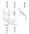
- Non-linear circuit 15 has the non-linear characteristics as shown in FIG. 5A and assuming that the stepped waveform image signal as shown in FIG. 5B is supplied to the said non-linear circuit 15, the image signal having the waveform as shown in FIG. 5C is output by the said non-linear circuit 15.
- the image signal given out by the non-linear circuit 15 has such characteristics that, as shown in FIG. 5C, the signal level is compressed for the signal indicating the dark area of the image (i.e., the area where signal level is small) and the signal indicating the bright area of the image (i.e., the area where signal level is large), while the signal level is expanded for the signal indicating the area where the brightness of the image is medium (i.e., at around the area where signal level is medium).
- the image signal indicated in FIG. 5C is supplied to the outline signal forming circuit 2 and outline signal E as shown in FIG. 5D is output by the outline signal forming circuit 2 and fed to the adder 5.
- the non-linear circuit 15 prior to the outline signal forming circuit 2, it is possible to suppress the amount of outline emphasis for the signals representing the dark part and bright part of the image and realize the optimum outline emphasis in a wide range from dark scene to the bright scene of the image and thus glittering in the dark scene or blooming (smashing of white or blurr) in the bright scene etc. are prevented and at the scene where the brightness is normal, an appropriate emphasis of the outline obtained.
- FIG. 6 is the drawing to show the composition of the outline correction circuit of such other embodiment.
- element 15 is a non-linear circuit
- 20 is an amplifier
- 21, 22 are differential circuit
- 22 is reversal amplifier
- 24 is delay circuit
- 25 is adder.
- image input signal A (see FIG. 7B) is given the signal waveform as shown in FIG. 7C by the non-linear circuit having the charateristics shown in FIG. 7A, amplified by amplifier 20, supplied to the outline signal forming circuit 26 which is composed of differential circuit 21, 23 and reversal amplifier 22 and the signal with such waveform as shown by FIG. 7C is formed by the said outline siganl forming circuit 26.
- input image signal A is delayed by the delay circuit 24 and supplied to adder 25.
- the output signal M of the outline signal forming circuit 26 (see FIG. 7E) and output signal N of delay circuit 24 (see FIG. 7F) are supplied to adder 25 and by adding these two, the image signal P (see FIG. 7G) which had been given the outline correction is obtained.
- the image signal P (see FIG. 7G) which had been given the outline correction is obtained.
- overshoot (c in the Figure) and preshoot (b in the Figure) are added to the input image signal and thus it is possible to display the image with even better sharpness.
- FIG. 8 is the drawing to show the composition of the outline correction circuit representing the second embodiment of the present invention.
- element 11 is the input terminal of image signal; 12 is the low-pass filter (LPF) for limiting the hand width to digitalize image signal; 13 is the analogue/ditigal (A/D) converter to change analogue signal into digital signal; 14 is the converter table to change digital signal into other digital signal which has the non-linear chracteristics and is composed of RAM (random access memory) to enable rewriting of the value of conversion table (non-linear characteristics).
- LPF low-pass filter
- A/D analogue/ditigal converter
- A/D analogue/ditigal converter to change analogue signal into digital signal
- 14 is the converter table to change digital signal into other digital signal which has the non-linear chracteristics and is composed of RAM (random access memory) to enable rewriting of the value of conversion table (non-linear characteristics).
- Element 15 is the control unit to supply the data for rewriting the value of the aforesaid conversion table 14 in order to obtain the outline emphasis preferred by the operator.
- Element 16 is the difference detection data processing circuit which compares the present image data with the image data one sample period prior thereto, forms the differential value data and when thus formed differential value data are smaller than the preset differential value level or when the polarity of the differential value data is reversed, adds the data of the same value but with reversed polarity to the said differential value data at the timing one sample period delayed; 17 is the adder circuit to add the differential value data output by the said difference detection data processing circuit 16 to the image data delayed by the delay circuit 11 to be stated later; 18 is the limiter circuit which prevents the image data output by the said adder circuit 17 exceed the black level peak (i.e., minimum value) or white level peak (i.e., maximum value), 19 is the digital/analogue (D/A) converter to convert the image data output by the said limiter circuit 18 into analogue signals; 20 is the low pass filter to limit the image signal to be output by the said D/A converter 19 within the desired band width and 21 is the delay circuit to delay the image data by one sample period.
- the band width of the image signal input by input terminal 11 is limited within the desired range by LPF12 and then it is converted into digital signal by A/D converter 13 and supplied to the difference detection data processing circuit 16.
- the difference detection data processing circuit 16 receives the present image data supplied by the said A/D converter 13 and the image data one sample period prior thereto which have been delayed by one sample period by the circuit 21 and the differential value data are comparatively detected.
- differential value data C (except the part marked by diagonal lines in the figure) is obtained by subtracting the present image data A from the image data B which have been delayed by one sample period.
- T1, T2, T3, T4 and T11 ?? T14 in the figure indicate the timing of sampling).
- Differential value data obtained from difference detection data processing circuit 16 of FIG. 8 are given non-linear conversion according to the conversion table 14.
- Non-linear conversion characteristics of the said conversion table 14 are such that, as shown in FIG. 9, when the level of the differential value data is lower than D1 in the figure, it is converted into the conversion value data indicating "0" and when the level of the said differential value data is higher than D2 in the figure, they are converted into the conversion value data indicating the preset level.
- Non-linear characteristics of the conversion table 14 use the RAM (random access memory) so that the composition can be changed in such way that they fit the outline emphasis level preferred by the operator according to the instruction given by the control unit 15.
- the difference detection data processing circuit 16 outputs the differential value data added with the part marked by diagonal lines in FIG. 10C.
- Such differential value data C are supplied to the adder circuit 7 while to such adder circuit 17 are already added the image data B having been delayed for one sample period by the delay circuit 21 and by addition of these two data, the image data D which are emphasized of the outline are formed and they are supplied to the limiter circuit 18.
- the image data are so limited that they become in between the white peak level (i.e., the maximum value of image data) and the black peak level (i.e., the minimum value of image data or when the said image data include the data obtained by digitalizing the synchronized signals, the value level which is lower than the pedestal level shown by the image data but within the range where synchronization does not become unstable) and thus limited data are output, converted into analogue signal at D/A converter 19, limited by LPE20 for their band and are output as the image signals with emphasized outline.
- the white peak level i.e., the maximum value of image data
- the black peak level i.e., the minimum value of image data or when the said image data include the data obtained by digitalizing the synchronized signals, the value level which is lower than the pedestal level shown by the image data but within the range where synchronization does not become unstable
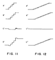
- FIG. 11 shows the signal waveforms at various units when the image signals having medium range frequency band and rising radically are input into the device shown in FIG. 8, while FIG. 12 shows the signal waveforms at various units when the image signals having the frequency band lower than the image signals indicated in FIG. 11 and rising moderately are input.
- FIG. 12 shows the signal waveforms at various units when the image signals having the frequency band lower than the image signals indicated in FIG. 11 and rising moderately are input.
- outline emphasis is not made on the moderately canning image signals and therefore there is no change of deterioration of picture quality.
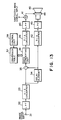
- FIG. 13 is the drawing to show the schematic composition of the TV image receiver to which the present invention has been applied, which represents the third embodiment of the present invention while FIG. 14 is the timing chart to describe the performance of the composition of the said FIG. 13.
- the element 31 is the image signal input terminal; 32 is the low pass filter (LPF) which, at the digitalization of the input image signal, limits the said image signal into the desired band; 33 is the analogue/digital (A/D) converter and 34 is the delay device to delay the digital signal output by said A/D converter 33 which comprises for example a memory.
- LPF low pass filter
- A/D analogue/digital
- Element 35 is the subtractor to obtain the differential value between the digital signal formed at the said A/D converter 33 and the digital signal formed one sampling period before; 36 is the data conversion unit to convert the difference value output by the said subtractor 35 based on the conversion data memorized at the conversion table 37 which is stated later; 37 is the conversion table memorizing the conversion data used for non-linear conversion of the difference value output by the said subtractor 35, the said conversion table being composed of RAM (Random Access Memory).
- Element 38 is the control unit to instruct rewriting of the conversion data to be memorized by the said conversion table 37 in order to obtain the picture quality designated by the operator;
- 39 is the digital/analogue (D/A) converter to convert the signal having been given non-linear conversion by the said data conversion unit 36 into analogue signal;
- 40 is the low pass filter (LPF) which limits the band of the signal output by the said D/A converter 39 into the desired band;
- 41 is the adder to add the signal output by the said LPF40 and the sawteeth wave signal for horizontal deflection;
- 42 is the digital/analogue (D/A) converter to convert the digital signal delayed by delay device 34 into analogue signal;
- 43 is the low pass filter (LPF) to limit the band of the signal output by the said D/A converter into the desired band;
- 44 is the deflection coil to deflect the electron beam modulated by the image signal;
- 45 is the image receiving tube (CRT) to display the image corresponding to the image sing
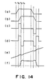
- the image signal input by the input terminal 31 is limited to the desired band by LPF32 and converted into digital signal by the A/D converter 33 which functions in synchronization with the sampling timing (T1, T2, T3 Vietnamese in the figure) shown in FIG. 14 and the image data output by the said A/D converter 33 (see FIG. 14a) are supplied to the subtractor 35 and delay device 34.
- the differential value (see FIG. 14(c)) between the signal being output by A/D converter 33 and the signal delayed for one sampling period by the said delay device 34 (see FIG. 14(b)) is output at the said subtractor 35.
- Differential value data output by the said subtractor 35 are the data non-linearly converted by the data conversion unit 36 based on the conversion data memorized by the conversion table 37.
- non-linear conversion characteristics of the said conversion table 37 are such that when the level of the differential value data supplied is larger than the preset value (D2 in the figure), conversion value data of preset level is output.
- the said conversion table 37 is composed of RAM stated above and it is so arranged that the conversion data which determines the non-linear characteristics according to the instruction of the control unit 38 of FIG. 13 can be rewritten and it is possible to set the conversion data according to the instruction of the operator.
- the differential value data non-linearly converted according to the conversion data memorized by the said conversion table 37 are added to the differential value data non-linearly converted as aforesaid, delayed by one sampling period and having the signal waveform with reversed polarity (see FIG. 14(d)).
- the signal formed at the said data conversion unit 36 is converted into an analogue signal by D/A converter 39, its band being limited by LPF40 and added with the sawteeth wave signal for horizontal deflection at adder 41 (see FIG. 14(e)) and supplied to deflection coil 44.
- the image data being output by the said delay device 34 is converted into analogue signal by D/A converter 42, its band being limited by LPF43 and supplied to CRT45 while the electron beam modulated by the image signal output by the said LPF43 is horizontally deflected by the said deflection coil 44.
- the action timing of the device is controlled to be synchronized with the sampling block and the action becomes extremely stable while by rewriting the contents of conversion table memorizing the conversion data for setting the nonlinear characteristics which determine the sharpness, the picture quality designated by the operator is easily obtained.
Applications Claiming Priority (6)
| Application Number | Priority Date | Filing Date | Title |
|---|---|---|---|
| JP2111964A JPH0410767A (ja) | 1990-04-27 | 1990-04-27 | 輪郭強調回路 |
| JP111964/90 | 1990-04-27 | ||
| JP2111977A JPH0410775A (ja) | 1990-04-27 | 1990-04-27 | テレビジョン受像機 |
| JP2111961A JPH0410774A (ja) | 1990-04-27 | 1990-04-27 | 輪郭補正装置 |
| JP111961/90 | 1990-04-27 | ||
| JP111977/90 | 1990-04-27 |
Publications (3)
| Publication Number | Publication Date |
|---|---|
| EP0454355A2 true EP0454355A2 (de) | 1991-10-30 |
| EP0454355A3 EP0454355A3 (en) | 1992-04-29 |
| EP0454355B1 EP0454355B1 (de) | 1996-12-27 |
Family
ID=27312136
Family Applications (1)
| Application Number | Title | Priority Date | Filing Date |
|---|---|---|---|
| EP91303461A Expired - Lifetime EP0454355B1 (de) | 1990-04-27 | 1991-04-18 | Gerät zur Verarbeitung von Bildsignalen zwecks Verbesserung der Kantensteilheit |
Country Status (4)
| Country | Link |
|---|---|
| US (1) | US5696852A (de) |
| EP (1) | EP0454355B1 (de) |
| CA (1) | CA2040881C (de) |
| DE (1) | DE69123780T2 (de) |
Cited By (1)
| Publication number | Priority date | Publication date | Assignee | Title |
|---|---|---|---|---|
| EP0693857A3 (de) * | 1994-07-18 | 1998-02-11 | Thomson Consumer Electronics, Inc. | Vorverarbeitungsgerät zum Eliminieren der Konturen bei Videokompressionssystemen |
Families Citing this family (37)
| Publication number | Priority date | Publication date | Assignee | Title |
|---|---|---|---|---|
| CA2231828C (en) * | 1995-09-28 | 2007-05-29 | Snell & Wilcox Limited | Video signal processing |
| JPH09214807A (ja) * | 1996-01-31 | 1997-08-15 | Canon Inc | 画像処理装置および画像処理方法 |
| JP3356201B2 (ja) * | 1996-04-12 | 2002-12-16 | ソニー株式会社 | ビデオカメラおよび輪郭強調装置 |
| JP3763901B2 (ja) * | 1996-10-17 | 2006-04-05 | 富士写真フイルム株式会社 | 画像情報読取装置 |
| JP4200890B2 (ja) * | 2003-12-10 | 2008-12-24 | 株式会社日立製作所 | 映像信号処理装置及びそれを用いたテレビジョン受信機並びに映像信号処理方法 |
| US7440633B2 (en) * | 2003-12-19 | 2008-10-21 | Sharp Laboratories Of America, Inc. | Enhancing the quality of decoded quantized images |
| US7424168B2 (en) * | 2003-12-24 | 2008-09-09 | Sharp Laboratories Of America, Inc. | Enhancing the quality of decoded quantized images |
| US7424166B2 (en) * | 2003-12-24 | 2008-09-09 | Sharp Laboratories Of America, Inc. | Enhancing the quality of decoded quantized images |
| US7400779B2 (en) * | 2004-01-08 | 2008-07-15 | Sharp Laboratories Of America, Inc. | Enhancing the quality of decoded quantized images |
| US8913089B2 (en) | 2005-06-15 | 2014-12-16 | Sharp Laboratories Of America, Inc. | Methods and systems for enhancing display characteristics with frequency-specific gain |
| US7982707B2 (en) | 2004-12-02 | 2011-07-19 | Sharp Laboratories Of America, Inc. | Methods and systems for generating and applying image tone scale adjustments |
| US7924261B2 (en) | 2004-12-02 | 2011-04-12 | Sharp Laboratories Of America, Inc. | Methods and systems for determining a display light source adjustment |
| US7800577B2 (en) | 2004-12-02 | 2010-09-21 | Sharp Laboratories Of America, Inc. | Methods and systems for enhancing display characteristics |
| US8120570B2 (en) | 2004-12-02 | 2012-02-21 | Sharp Laboratories Of America, Inc. | Systems and methods for tone curve generation, selection and application |
| US7515160B2 (en) | 2006-07-28 | 2009-04-07 | Sharp Laboratories Of America, Inc. | Systems and methods for color preservation with image tone scale corrections |
| US7782405B2 (en) | 2004-12-02 | 2010-08-24 | Sharp Laboratories Of America, Inc. | Systems and methods for selecting a display source light illumination level |
| US7961199B2 (en) | 2004-12-02 | 2011-06-14 | Sharp Laboratories Of America, Inc. | Methods and systems for image-specific tone scale adjustment and light-source control |
| US8947465B2 (en) | 2004-12-02 | 2015-02-03 | Sharp Laboratories Of America, Inc. | Methods and systems for display-mode-dependent brightness preservation |
| US8922594B2 (en) | 2005-06-15 | 2014-12-30 | Sharp Laboratories Of America, Inc. | Methods and systems for enhancing display characteristics with high frequency contrast enhancement |
| US8004511B2 (en) | 2004-12-02 | 2011-08-23 | Sharp Laboratories Of America, Inc. | Systems and methods for distortion-related source light management |
| US9083969B2 (en) | 2005-08-12 | 2015-07-14 | Sharp Laboratories Of America, Inc. | Methods and systems for independent view adjustment in multiple-view displays |
| US7768496B2 (en) | 2004-12-02 | 2010-08-03 | Sharp Laboratories Of America, Inc. | Methods and systems for image tonescale adjustment to compensate for a reduced source light power level |
| US7839406B2 (en) | 2006-03-08 | 2010-11-23 | Sharp Laboratories Of America, Inc. | Methods and systems for enhancing display characteristics with ambient illumination input |
| US7375573B2 (en) * | 2006-05-25 | 2008-05-20 | Micron Technology, Inc. | De-emphasis system and method for coupling digital signals through capacitively loaded lines |
| US7826681B2 (en) | 2007-02-28 | 2010-11-02 | Sharp Laboratories Of America, Inc. | Methods and systems for surround-specific display modeling |
| US8155434B2 (en) | 2007-10-30 | 2012-04-10 | Sharp Laboratories Of America, Inc. | Methods and systems for image enhancement |
| US9177509B2 (en) | 2007-11-30 | 2015-11-03 | Sharp Laboratories Of America, Inc. | Methods and systems for backlight modulation with scene-cut detection |
| US8378956B2 (en) | 2007-11-30 | 2013-02-19 | Sharp Laboratories Of America, Inc. | Methods and systems for weighted-error-vector-based source light selection |
| US8207932B2 (en) | 2007-12-26 | 2012-06-26 | Sharp Laboratories Of America, Inc. | Methods and systems for display source light illumination level selection |
| US8169431B2 (en) | 2007-12-26 | 2012-05-01 | Sharp Laboratories Of America, Inc. | Methods and systems for image tonescale design |
| US8179363B2 (en) | 2007-12-26 | 2012-05-15 | Sharp Laboratories Of America, Inc. | Methods and systems for display source light management with histogram manipulation |
| US8203579B2 (en) | 2007-12-26 | 2012-06-19 | Sharp Laboratories Of America, Inc. | Methods and systems for backlight modulation with image characteristic mapping |
| US8223113B2 (en) | 2007-12-26 | 2012-07-17 | Sharp Laboratories Of America, Inc. | Methods and systems for display source light management with variable delay |
| US8531379B2 (en) | 2008-04-28 | 2013-09-10 | Sharp Laboratories Of America, Inc. | Methods and systems for image compensation for ambient conditions |
| US8416179B2 (en) | 2008-07-10 | 2013-04-09 | Sharp Laboratories Of America, Inc. | Methods and systems for color preservation with a color-modulated backlight |
| US9330630B2 (en) | 2008-08-30 | 2016-05-03 | Sharp Laboratories Of America, Inc. | Methods and systems for display source light management with rate change control |
| US8165724B2 (en) | 2009-06-17 | 2012-04-24 | Sharp Laboratories Of America, Inc. | Methods and systems for power-controlling display devices |
Citations (4)
| Publication number | Priority date | Publication date | Assignee | Title |
|---|---|---|---|---|
| US4422094A (en) * | 1981-11-06 | 1983-12-20 | Rca Corporation | Digital signal processor with symmetrical transfer characteristic |
| EP0201245A2 (de) * | 1985-04-30 | 1986-12-17 | RCA Thomson Licensing Corporation | Umwandler von Zeilensprungabtastung in fortlaufende Abtastung für RGB-Art-Videoeingangssignale |
| JPS62299180A (ja) * | 1986-06-18 | 1987-12-26 | Mitsubishi Electric Corp | 適応型輪郭補正装置 |
| EP0340648A2 (de) * | 1988-04-30 | 1989-11-08 | Victor Company Of Japan, Limited | Schaltung zur Verbesserung der Bildqualität |
Family Cites Families (5)
| Publication number | Priority date | Publication date | Assignee | Title |
|---|---|---|---|---|
| JPH0143510B2 (de) * | 1978-09-28 | 1989-09-21 | Eastman Kodak Co | |
| JPS6276871A (ja) * | 1985-09-30 | 1987-04-08 | Toshiba Corp | 画質補正回路 |
| US4849826A (en) * | 1986-11-14 | 1989-07-18 | Matsushita Electric Industrial Co., Ltd. | Digital non-linear pre-emphasis/de-emphasis apparatus for eliminating noise components from video signals in a video signal processing system |
| DE68922433T2 (de) * | 1988-05-18 | 1996-01-11 | Hitachi Ltd | Aporturkorrekturschaltung. |
| KR930002906B1 (ko) * | 1989-12-23 | 1993-04-15 | 삼성전자 주식회사 | 윤곽 보정회로 |
-
1991
- 1991-04-18 DE DE69123780T patent/DE69123780T2/de not_active Expired - Fee Related
- 1991-04-18 EP EP91303461A patent/EP0454355B1/de not_active Expired - Lifetime
- 1991-04-19 CA CA002040881A patent/CA2040881C/en not_active Expired - Fee Related
-
1995
- 1995-03-31 US US08/414,572 patent/US5696852A/en not_active Expired - Fee Related
Patent Citations (4)
| Publication number | Priority date | Publication date | Assignee | Title |
|---|---|---|---|---|
| US4422094A (en) * | 1981-11-06 | 1983-12-20 | Rca Corporation | Digital signal processor with symmetrical transfer characteristic |
| EP0201245A2 (de) * | 1985-04-30 | 1986-12-17 | RCA Thomson Licensing Corporation | Umwandler von Zeilensprungabtastung in fortlaufende Abtastung für RGB-Art-Videoeingangssignale |
| JPS62299180A (ja) * | 1986-06-18 | 1987-12-26 | Mitsubishi Electric Corp | 適応型輪郭補正装置 |
| EP0340648A2 (de) * | 1988-04-30 | 1989-11-08 | Victor Company Of Japan, Limited | Schaltung zur Verbesserung der Bildqualität |
Non-Patent Citations (1)
| Title |
|---|
| PATENT ABSTRACTS OF JAPAN, vol. 12, no. 200 (E-619), 9th June 1988; & JP-A-62 299 180 (MITSUBISHI) 26-12-1987 * |
Cited By (1)
| Publication number | Priority date | Publication date | Assignee | Title |
|---|---|---|---|---|
| EP0693857A3 (de) * | 1994-07-18 | 1998-02-11 | Thomson Consumer Electronics, Inc. | Vorverarbeitungsgerät zum Eliminieren der Konturen bei Videokompressionssystemen |
Also Published As
| Publication number | Publication date |
|---|---|
| DE69123780D1 (de) | 1997-02-06 |
| US5696852A (en) | 1997-12-09 |
| CA2040881A1 (en) | 1991-10-28 |
| CA2040881C (en) | 1995-08-22 |
| EP0454355A3 (en) | 1992-04-29 |
| DE69123780T2 (de) | 1997-05-07 |
| EP0454355B1 (de) | 1996-12-27 |
Similar Documents
| Publication | Publication Date | Title |
|---|---|---|
| US5696852A (en) | Image signal processing apparatus | |
| US5394195A (en) | Method and apparatus for performing dynamic gamma contrast control | |
| US20030206241A1 (en) | Imaging apparatus with dynamic range expanded, a video camera including the same, and a method of generating a dynamic range expanded video signal | |
| US5237414A (en) | Video enhancer with separate processing of high and low level transitions | |
| KR0143389B1 (ko) | 윤곽보정장치 | |
| EP0720391B1 (de) | Digitale Verarbeitungsvorrichtung | |
| US5121209A (en) | Sharpness control for a television image | |
| JPH05308592A (ja) | ビデオ信号処理装置 | |
| US5146319A (en) | Digital luminance signal transient improver and peaker | |
| US5444500A (en) | Display device including a correction circuit, and correction circuit for use in a display device | |
| US7064794B2 (en) | Method for dynamic contrast improvement | |
| US5218438A (en) | Picture aperture correction circuit | |
| EP0633690A2 (de) | Schaltung zum Wiederherstellen des Schwarzwertes für einen Fernsehempfänger | |
| US5223920A (en) | Video processor having automatic chrominance control compensation | |
| US4802010A (en) | Method and apparatus for generating an adaptive peaking signal increasing the sharpness of a video signal | |
| US3919471A (en) | TV signal correction circuitry | |
| EP0598442B1 (de) | Wiedergabeanordnung mit einer Korrekturschaltung und Korrekturschaltung zum Gebrauch in einer solchen Anordnung | |
| JPH0316078B2 (de) | ||
| JP2935389B2 (ja) | 映像信号処理装置及び非線形信号処理装置 | |
| JP3087409B2 (ja) | 階調補正装置 | |
| JP2830587B2 (ja) | 映像信号処理装置 | |
| EP0268332B1 (de) | Verfahren und Schaltung zur Erzeugung eines anpassungsfähigen Anhebungssignals zur Vergrösserung der Schärfe eines Videosignals | |
| JPH0690382A (ja) | 階調補正装置 | |
| JPH0662278A (ja) | 映像信号処理装置 | |
| JPH0410774A (ja) | 輪郭補正装置 |
Legal Events
| Date | Code | Title | Description |
|---|---|---|---|
| PUAI | Public reference made under article 153(3) epc to a published international application that has entered the european phase |
Free format text: ORIGINAL CODE: 0009012 |
|
| AK | Designated contracting states |
Kind code of ref document: A2 Designated state(s): DE FR GB IT NL |
|
| PUAL | Search report despatched |
Free format text: ORIGINAL CODE: 0009013 |
|
| AK | Designated contracting states |
Kind code of ref document: A3 Designated state(s): DE FR GB IT NL |
|
| 17P | Request for examination filed |
Effective date: 19920909 |
|
| 17Q | First examination report despatched |
Effective date: 19940801 |
|
| GRAG | Despatch of communication of intention to grant |
Free format text: ORIGINAL CODE: EPIDOS AGRA |
|
| GRAH | Despatch of communication of intention to grant a patent |
Free format text: ORIGINAL CODE: EPIDOS IGRA |
|
| GRAH | Despatch of communication of intention to grant a patent |
Free format text: ORIGINAL CODE: EPIDOS IGRA |
|
| GRAA | (expected) grant |
Free format text: ORIGINAL CODE: 0009210 |
|
| AK | Designated contracting states |
Kind code of ref document: B1 Designated state(s): DE FR GB IT NL |
|
| PG25 | Lapsed in a contracting state [announced via postgrant information from national office to epo] |
Ref country code: IT Free format text: LAPSE BECAUSE OF FAILURE TO SUBMIT A TRANSLATION OF THE DESCRIPTION OR TO PAY THE FEE WITHIN THE PRE;WARNING: LAPSES OF ITALIAN PATENTS WITH EFFECTIVE DATE BEFORE 2007 MAY HAVE OCCURRED AT ANY TIME BEFORE 2007. THE CORRECT EFFECTIVE DATE MAY BE DIFFERENT FROM THE ONE RECORDED.SCRIBED TIME-LIMIT Effective date: 19961227 |
|
| REF | Corresponds to: |
Ref document number: 69123780 Country of ref document: DE Date of ref document: 19970206 |
|
| ET | Fr: translation filed | ||
| PLBE | No opposition filed within time limit |
Free format text: ORIGINAL CODE: 0009261 |
|
| STAA | Information on the status of an ep patent application or granted ep patent |
Free format text: STATUS: NO OPPOSITION FILED WITHIN TIME LIMIT |
|
| 26N | No opposition filed | ||
| REG | Reference to a national code |
Ref country code: GB Ref legal event code: IF02 |
|
| PGFP | Annual fee paid to national office [announced via postgrant information from national office to epo] |
Ref country code: NL Payment date: 20040415 Year of fee payment: 14 |
|
| PGFP | Annual fee paid to national office [announced via postgrant information from national office to epo] |
Ref country code: DE Payment date: 20040421 Year of fee payment: 14 Ref country code: FR Payment date: 20040421 Year of fee payment: 14 |
|
| PGFP | Annual fee paid to national office [announced via postgrant information from national office to epo] |
Ref country code: GB Payment date: 20050404 Year of fee payment: 15 |
|
| PG25 | Lapsed in a contracting state [announced via postgrant information from national office to epo] |
Ref country code: NL Free format text: LAPSE BECAUSE OF NON-PAYMENT OF DUE FEES Effective date: 20051101 Ref country code: DE Free format text: LAPSE BECAUSE OF NON-PAYMENT OF DUE FEES Effective date: 20051101 |
|
| PG25 | Lapsed in a contracting state [announced via postgrant information from national office to epo] |
Ref country code: FR Free format text: LAPSE BECAUSE OF NON-PAYMENT OF DUE FEES Effective date: 20051230 |
|
| NLV4 | Nl: lapsed or anulled due to non-payment of the annual fee |
Effective date: 20051101 |
|
| REG | Reference to a national code |
Ref country code: FR Ref legal event code: ST Effective date: 20051230 |
|
| PG25 | Lapsed in a contracting state [announced via postgrant information from national office to epo] |
Ref country code: GB Free format text: LAPSE BECAUSE OF NON-PAYMENT OF DUE FEES Effective date: 20060418 |
|
| GBPC | Gb: european patent ceased through non-payment of renewal fee |
Effective date: 20060418 |