EP0454055B1 - Semiconductor device and method for manufacturing the same - Google Patents
Semiconductor device and method for manufacturing the same Download PDFInfo
- Publication number
- EP0454055B1 EP0454055B1 EP91106512A EP91106512A EP0454055B1 EP 0454055 B1 EP0454055 B1 EP 0454055B1 EP 91106512 A EP91106512 A EP 91106512A EP 91106512 A EP91106512 A EP 91106512A EP 0454055 B1 EP0454055 B1 EP 0454055B1
- Authority
- EP
- European Patent Office
- Prior art keywords
- film
- impurity
- single crystal
- crystal silicon
- polysilicon film
- Prior art date
- Legal status (The legal status is an assumption and is not a legal conclusion. Google has not performed a legal analysis and makes no representation as to the accuracy of the status listed.)
- Expired - Lifetime
Links
Images


Classifications
-
- H—ELECTRICITY
- H01—ELECTRIC ELEMENTS
- H01L—SEMICONDUCTOR DEVICES NOT COVERED BY CLASS H10
- H01L21/00—Processes or apparatus adapted for the manufacture or treatment of semiconductor or solid state devices or of parts thereof
- H01L21/02—Manufacture or treatment of semiconductor devices or of parts thereof
- H01L21/04—Manufacture or treatment of semiconductor devices or of parts thereof the devices having at least one potential-jump barrier or surface barrier, e.g. PN junction, depletion layer or carrier concentration layer
- H01L21/18—Manufacture or treatment of semiconductor devices or of parts thereof the devices having at least one potential-jump barrier or surface barrier, e.g. PN junction, depletion layer or carrier concentration layer the devices having semiconductor bodies comprising elements of Group IV of the Periodic System or AIIIBV compounds with or without impurities, e.g. doping materials
- H01L21/30—Treatment of semiconductor bodies using processes or apparatus not provided for in groups H01L21/20 - H01L21/26
- H01L21/31—Treatment of semiconductor bodies using processes or apparatus not provided for in groups H01L21/20 - H01L21/26 to form insulating layers thereon, e.g. for masking or by using photolithographic techniques; After treatment of these layers; Selection of materials for these layers
- H01L21/3205—Deposition of non-insulating-, e.g. conductive- or resistive-, layers on insulating layers; After-treatment of these layers
- H01L21/321—After treatment
- H01L21/3215—Doping the layers
- H01L21/32155—Doping polycristalline - or amorphous silicon layers
-
- H—ELECTRICITY
- H01—ELECTRIC ELEMENTS
- H01L—SEMICONDUCTOR DEVICES NOT COVERED BY CLASS H10
- H01L21/00—Processes or apparatus adapted for the manufacture or treatment of semiconductor or solid state devices or of parts thereof
- H01L21/02—Manufacture or treatment of semiconductor devices or of parts thereof
- H01L21/04—Manufacture or treatment of semiconductor devices or of parts thereof the devices having at least one potential-jump barrier or surface barrier, e.g. PN junction, depletion layer or carrier concentration layer
- H01L21/18—Manufacture or treatment of semiconductor devices or of parts thereof the devices having at least one potential-jump barrier or surface barrier, e.g. PN junction, depletion layer or carrier concentration layer the devices having semiconductor bodies comprising elements of Group IV of the Periodic System or AIIIBV compounds with or without impurities, e.g. doping materials
- H01L21/20—Deposition of semiconductor materials on a substrate, e.g. epitaxial growth solid phase epitaxy
- H01L21/203—Deposition of semiconductor materials on a substrate, e.g. epitaxial growth solid phase epitaxy using physical deposition, e.g. vacuum deposition, sputtering
-
- H—ELECTRICITY
- H01—ELECTRIC ELEMENTS
- H01L—SEMICONDUCTOR DEVICES NOT COVERED BY CLASS H10
- H01L21/00—Processes or apparatus adapted for the manufacture or treatment of semiconductor or solid state devices or of parts thereof
- H01L21/02—Manufacture or treatment of semiconductor devices or of parts thereof
- H01L21/04—Manufacture or treatment of semiconductor devices or of parts thereof the devices having at least one potential-jump barrier or surface barrier, e.g. PN junction, depletion layer or carrier concentration layer
- H01L21/18—Manufacture or treatment of semiconductor devices or of parts thereof the devices having at least one potential-jump barrier or surface barrier, e.g. PN junction, depletion layer or carrier concentration layer the devices having semiconductor bodies comprising elements of Group IV of the Periodic System or AIIIBV compounds with or without impurities, e.g. doping materials
- H01L21/30—Treatment of semiconductor bodies using processes or apparatus not provided for in groups H01L21/20 - H01L21/26
- H01L21/31—Treatment of semiconductor bodies using processes or apparatus not provided for in groups H01L21/20 - H01L21/26 to form insulating layers thereon, e.g. for masking or by using photolithographic techniques; After treatment of these layers; Selection of materials for these layers
- H01L21/3205—Deposition of non-insulating-, e.g. conductive- or resistive-, layers on insulating layers; After-treatment of these layers
- H01L21/32055—Deposition of semiconductive layers, e.g. poly - or amorphous silicon layers
Definitions
- This invention relates to a semiconductor device manufacturing method according to the preamble of claim 1.
- an electrode or electrode wiring formed of a polysilicon film as a main component is formed on an insulation film on the main surface area of a semiconductor substrate (wafer), and an additional insulation film is often formed on the same.
- impurity such as phosphorus (P) is generally doped into the polysilicon film to lower the resistance thereof so that it can be used for a desired purpose.
- P phosphorus
- a polysilicon film containing impurity is first formed by deposition on the semiconductor substrate, the semiconductor substrate is heated to a temperature of higher than 600°C to thermally diffuse phosphorus while the surface of the polysilicon film is being oxidized, and then the oxide film on the surface of the polysilicon film is removed by use of chemical such as hydrofluoric acid.
- the above method has defects that variation in the concentration of phosphorus contained in the polysilicon film is large in the surface area of the substrate (in the surface area of the wafer) and it is difficult to increase the diameter of the semiconductor substrate and since the oxide film formed on the polysilicon film is removed by use of chemical after phosphorus is diffused, the chemical may damage the underground layer through the grain boundary of the polysilicon film when the polysilicon film is formed to be thinner with increasing miniaturization of the element.
- Fig. 1 schematically shows a general construction of a low pressure CVD (chemical vapor deposition) device used when effecting the in-situ doping method.
- 91 denotes a low pressure CVD furnace
- 92, 92, --- denote semiconductor substrates (wafers) disposed in the CVD furnace
- 93 denotes a sample table (boat) for holding a group of semiconductor substrates in a horizontal position
- 94 denotes a gas inlet port for permitting silane (SiH 4 ) gas to be supplied into the CVD furnace via the lower portion thereof
- 95 denotes a gas inlet port for permitting phosphine (PH 3 ) gas to be supplied into the CVD furnace via the lower portion thereof
- 96 denotes an exhaust port provided on the upper portion of the CVD furnace.
- SiH 4 gas and PH 3 gas are simultaneously introduced into the CVD furnace so as to form a polysilicon film by deposition and at the same time dope phosphorus.
- uniformity of phosphorus concentration of the polysilicon film in the surface area of the substrate can be improved to some extent, it is necessary to use a special sample table on which the semiconductor substrates are mounted and pay special attention to the flow of gas, and in a case where an ordinary sample table is used, variation in the film thickness of the polysilicon film in the substrate surface area and variation in the phosphorus concentration in the polysilicon film will become large. Further, even when a special sample table is used, the deposition speed and phosphorus concentration may become non-uniform depending on the depositing position (distance from the gas inlet port) inside the CVD furnace.
- Fig. 2 shows an example of variation in the film thickness of the polysilicon film in the substrate surface area and variation in the phosphorus concentration of the polysilicon film in the substrate surface area.
- Fig. 3 shows an example of a condition wherein the deposition speed of the polysilicon film and the concentration of phosphorus in the polysilicon film become non-uniform depending on the position (distance from the gas inlet port) of the semiconductor substrate inside the low pressure CVD furnace, that is, the trend of variation in the properties of semiconductor substrates.
- This phenomenon is considered to occur because the attachment probability of semiconductor atoms (Si in this embodiment) when phosphorus is adsorbed on the surface is small so as to lower the deposition speed and the concentration distribution of phosphorus becomes non-uniform since the speed of decomposition of PH 3 gas for supplying impurity and the speed of decomposition of SiH 4 for depositing silicon are different to make the concentration distribution of phosphorus non-uniform.
- the deposition speed of the polysilicon film and the phosphorus concentration in the polysilicon film become non-uniform depending on the position of the semiconductor substrate inside the low pressure CVD furnace.
- Fig. 4 shows an example of variation in the withstanding voltage of the thermal oxide film in the substrate surface area and variation in the phosphorus concentration of the polysilicon film in the substrate surface area.
- a method of manufacturing the conventional semiconductor device has problems that when a polysilicon film containing impurity is formed on a semiconductor substrate in which the entire portion or part of the main surface area is covered with an insulation film, variation in the impurity concentration of the polysilicon film in the substrate surface area becomes large so that the profile of the impurity concentration of the polysilicon film formed in a contact hole which is formed in part of an insulation film formed on the substrate or a trench which is formed in part of the substrate may become non-uniform in the depth direction thereof and variation in the withstanding voltage of an insulation film to be formed on the polysilicon film becomes large.
- a method of manufacturing the semiconductor device including the conventional in-situ doping method has a problem that the deposition speed of a polysilicon film and the phosphorus concentration in the polysilicon film become non-uniform depending on the position of the semiconductor substrate inside the low pressure CVD furnace.
- An object of this invention is to provide a semiconductor device manufacturing method by which the impurity concentration of a polysilicon film containing impurity can be made uniform in the substrate surface area without using a special furnace structure or control of gas flow when the polysilicon film is formed on the semiconductor substrate whose main surface is at least partly covered with an insulation film in a low pressure CVD device.
- Another object of this invention is to provide a semiconductor device manufacturing method by which the deposition speed of a polysilicon film containing impurity or the impurity concentration of a polysilicon film can be prevented from being made non-uniform depending on the position of a semiconductor substrate inside a low pressure CVD furnace when the polysilicon film is formed on the semiconductor substrate whose main surface is at least partly covered with an insulation film in a low pressure CVD device.
- Fig. 5 shows an example of the structure of a capacitor formed on the main surface of a semiconductor substrate.
- 11 denotes a silicon substrate
- 12 denotes a first insulation film
- 17 denotes a first polysilicon film used as one of the electrodes of the capacitor
- 16 denotes a second insulation film serving as a dielectric layer of the capacitor
- 18 denotes a second polysilicon serving as the other electrode of the capacitor.
- phosphorus is contained as impurity in the first polysilicon film 17 serving as one of the electrodes.
- the impurity concentration in the depth direction of the first polysilicon film 17 is made uniform.
- the first insulation film (thermal oxide film) 12 with a film thickness of 50 nm (500 ⁇ ) is formed on the entire portion of the main surface of the silicon substrate 11.
- the silicon substrate is disposed in a horizontal position in a low pressure CVD device as shown in Fig. 1, the reaction temperature is set at 610°C and air is exhausted from the upper portion by means of a vacuum pump.
- the pressure at this time can be set in a range of 0.13 Pa to 1.33.10 4 Pa (0.001 Torr to 100 Torr) and in this embodiment, the pressure is set at 66.6 Pa (0.5 Torr), and a polysilicon film 13 containing no impurity is formed to a thickness of at least 10 nm (100 ⁇ ) on the first insulation film 12 by introducing SiH 4 gas from the lower portion and thermally decomposing the same on and over the first insulation film 12.
- SiH 4 gas from the lower portion and thermally decomposing the same on and over the first insulation film 12.
- PH 3 gas is passed under the reaction pressure of 66.6 Pa (0.5 Torr) and thermally decomposed on and over the polysilicon film 13 to adsorb and diffuse phosphorus on and near the surface of the polysilicon film so as to form a mono-layer 14 of phosphorus as shown in Fig. 6C after the above step, that is, without exposing the ( substrate to the outside air.
- SiH 4 gas is thermally decomposed on and over the polysilicon film 13 at the reaction temperature of 610°C to deposit a polysilicon film 15 as shown in Fig. 6D after the above step, that is, without exposing the substrate to the outside air.
- the polysilicon film 15 is thermally oxidized at a temperature of approx. 1000°C to form the second insulation film (thermal oxide film) 16 with a thickness of approx. 30 nm (300 ⁇ ) on the surface thereof.
- the second insulation film 16 serves as the dielectric layer of the capacitor.
- phosphorus of the mono-layer 14 is diffused into the polysilicon films 13 and 15 by the heat treatment in this step so that the polysilicon films 13 and 15 may be integrated and the resistance thereof will be lowered to form the first polysilicon film 17.
- the first polysilicon film 17 serves as one of the electrodes of the capacitor. In this case, the thickness of the first polysilicon film 17 is 20 nm (200 ⁇ ) and the average concentration of phosphorus in the first polysilicon film 17 is 5 ⁇ 10 20 cm -3 .
- the second polysilicon film 18 having a thickness of approx. 350 nm (3500 ⁇ ) and surface resistance of approx. 20 ⁇ and serving as the other electrode of the capacitor is formed on the second insulation film 16.
- the second polysilicon film 18, second insulation film 16 and first polysilicon film 17 are selectively etched by the photoetching process to form the capacitor as shown in Fig. 6G.
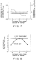
- Fig. 7 shows an example of the result of measurement of variation in the film thickness of the first polysilicon film of the capacitor formed in the above-described manner in the substrate surface area and variation in the phosphorus concentration of the first polysilicon film 17 in the substrate surface area. It is understood from Fig. 7 that the above variations are significantly improved in comparison with those for a polysilicon film formed by the in-situ doping method in which SiH 4 gas and PH 3 gas are simultaneously introduced.
- Fig. 8 shows an example of the result of measurement and comparison of a holding voltage of a capacitor formed in the above-described manner and that of a capacitor formed by the conventional method.
- the ordinate indicates the withstanding voltage of the second insulation film 16 by the intensity of electric field when a voltage is applied between the first polysilicon film 17 and the second polysilicon film 18 and the abscissa indicates the position in the substrate surface area.
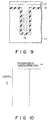
- Fig. 9 is a sectional view showing a semiconductor device according to a second embodiment of the invention. Many of the components of this device are identical to those of the device shown in Fig. 5, and will therefore be designated at the same numerals as those used in Fig. 5 and will not be described in detail.
- a trench 19 is formed in a silicon substrate 11.
- the trench 19 has a rectangular cross section, and its both sides extend vertically.
- a first insulation film 12 is formed in this trench 19.
- a polysilicon film 17 is formed on the insulation film 12 and, hence, in the trench 19, and also on the surface of the silicon substrate 11.
- the polysilicon film 17 also contains an impurity such as phosphorus.
- impurity concentration i.e., phosphorus concentration
- the first step of forming the first polysilicon film 13 containing no impurity on the semiconductor substrate in which at least part of the main surface is covered with the insulation film is effected, then the second step of forming the impurity layer on the surface of the polysilicon film 13 by passing gas containing desired impurity on and over the semiconductor substrate is effected, and the first step is repeatedly effected.
- the polysilicon film 17 it is possible to form the polysilicon film 17 to a desired thickness by repeatedly effecting the first and second steps by a desired number of times.
- Figs. 11A to 11F show respective steps of a method including the above steps and according to a third embodiment of this invention. That is, as shown in Fig. 11A, a first insulation film 12 with a thickness of 50 nm (500 ⁇ ) is formed on the entire portion of the main surface of a silicon substrate 11 in the same manner as in a case shown in Fig. 6A.
- the silicon substrate is placed in a horizontal position in a low pressure CVD device and a polysilicon film 13 containing no impurity is deposited on the first insulation film 12 in the same manner as in a case shown in Fig. 6B.
- PH 3 gas is passed under the reaction pressure of 66.6 Pa (0.5 Torr) and thermally decomposed on and over the polysilicon film 13 to adsorb and diffuse phosphorus on and near the surface portion of the polysilicon film so as to form a first mono-layer 14 1 of phosphorus after the above step, that is, without exposing the substrate to the outside air.
- SiH4 gas is thermally decomposed on and over the polysilicon film 13 at the reaction temperature of 610°C to deposit a polysilicon film 15 1 without exposing the substrate to the outside air.
- a second mono-layer 14 2 is formed on the polysilicon film 15 1 in the same manner as described above and then a polysilicon film 15 2 is deposited on the mono-layer.
- the polysilicon film 15 2 is thermally oxidized at a temperature of approx. 1000°C to form a second insulation film (thermal oxide film) 16 with a thickness of approx. 30 nm (300 ⁇ ) on the surface thereof.
- the second insulation film 16 serves as the dielectric layer of the capacitor.
- phosphorus of the first and second mono-layers 14 1 and 14 2 is diffused into the polysilicon films 13, 15 1 and 15 2 by the heat treatment in this step so that the polysilicon films 13, 15 1 and 15 2 may be integrated and the resistance thereof will be lowered to form a first polysilicon film 17'.
- the first polysilicon film 17' serves as one of the electrodes of the capacitor.
- a second polysilicon film 18 having a thickness of approx. 350 nm (3500 ⁇ ) and surface resistance of approx. 20 ⁇ and serving as the other electrode of the capacitor is formed on the first polysilicon film 17'.
- the second polysilicon film 18, second insulation film 16 and first polysilicon film 17' are sequentially and selectively etched by the photoetching process to form the capacitor as shown in Fig. 11F.
- the thicknesses of the polysilicon films 13, 15 1 and 15 2 are determined so as to set the average concentration of impurity in the original polysilicon films 13, 15 1 and 15 2 constituting the first polysilicon film 17' to a desired value.
- the polysilicon film 17 or 17' is formed on the silicon substrate in which the entire portion of the main surface is covered with the first insulation film 12.
- an example of a method of forming a polysilicon film on a semiconductor substrate having an impurity region formed in the substrate surface area under an opening which is formed in the first insulation film is explained as a fourth embodiment with reference to Figs. 12A to 12F.
- a first insulation film (thermal oxide film) 42 is formed to a thickness of 50 nm (500 ⁇ ) on the entire portion of the main surface of a P - -type silicon substrate 41. Then, As ions are ion-implanted into the silicon substrate 41 through the first insulation film 42 and heat treatment is effected to diffuse the As ions so as to form an N + -type region 43 in part of the silicon substrate 41.
- a contact hole 44 is formed in the first insulation film 42 on the N + -type region 43 and then SiH 4 gas is thermally decomposed on and over the insulation film 42 at the reaction temperature of 610°C and under the reaction pressure of 66.6 Pa (0.5 Torr) in the low pressure CVD device to deposit a polysilicon film 45 containing no impurity on the first insulation film 42 and in the contact hole 44.
- PH 3 gas is thermally decomposed on and over the polysilicon film 45 under the reaction pressure of 66.6 Pa (0.5 Torr) in the low pressure CVD device to form a mono-layer 46 of phosphorus on the surface of the polysilicon film.
- SiH 4 gas is thermally decomposed on and over the insulation film 45 at the reaction temperature of 610°C in the low pressure CVD device to deposit a polysilicon film 47 as shown in Fig. 12D.
- a passivation film for example, a phosphorus-silicate-glass film : PSG film
- a passivation film 48 is formed on the entire surface of the substrate. Further, phosphorus contained in the mono-layer 46 of phosphorus is diffused into the polysilicon films 45 and 47 in the heat treatment process in which the passivation film 48 is formed and a later melting step is effected, thereby integrating the polysilicon films 45 and 47 and lowering the resistance thereof to form a polysilicon film 49.
- the polysilicon film 49 serves as an electrode lead-out wiring extending from the N + -type region 43.
- the passivation film 48 is selectively etched to form a contact hole, and then an aluminum-silicon film is formed on the entire surface of the substrate and patterned to form an electrode 50.
- Fig. 13 shows an example of the result of measurement of electrical resistance of the polysilicon film 49 of the element formed in the above-described manner.
- variation in the electrical resistance in the substrate surface area is smaller in the case of the polysilicon film 49 formed by the method of the fourth embodiment than in the case of the polysilicon film formed by the conventional method and a proper electrical characteristic can be attained. This is considered to be because phosphorus is uniformly doped in the polysilicon film 49.
- a method according to a fifth embodiment of this invention is explained.
- the method of this embodiment is to form a polysilicon film containing impurity on a semiconductor substrate in which part of the main surface is covered with an insulation film and the other portion is exposed to a conductive layer.
- a semiconductor structure shown in Fig. 14A is formed.
- 61 denotes a P - -type silicon substrate, 62 a first insulation film, 63 an N + -type region, 64 a polysilicon film containing impurity, 65 a conductive film formed of, for example, MoSi, and 66 a second insulation film.
- the polysilicon film 64 is formed by the same method as that for forming the polysilicon film 49 in the fourth embodiment.
- part of a second insulation film 66 is etched to form a via-hole and then SiH 4 gas is thermally decomposed on and over the second insulation film 66 at the reaction temperature of 610°C and under the reaction pressure of 66.6 Pa (0.5 Torr) in the low pressure CVD device to deposit a polysilicon film 67 containing no impurity on the second insulation film 66.
- PH 3 gas is thermally decomposed on and over the polysilicon film 67 under the reaction pressure of 66.6 Pa (0.5 Torr) in the low pressure CVD device to form a mono-layer 68 of phosphorus on the surface of the polysilicon film.
- SiH 4 gas is thermally decomposed on and over the polysilicon film 68 at the reaction temperature of 610°C in the low pressure CVD device to deposit a polysilicon film 69 as shown in Fig. 14C.
- the semiconductor structure is subjected to the annealing process at a high temperature to diffuse phosphorus of the mono-layer 68 into the polysilicon films 67 and 69, thereby integrating the polysilicon films 67 and 69 and lowering the resistance thereof to form a polysilicon film 70.
- the polysilicon film 70 serves as a lead-out wiring of the conductive film 65 formed of MoSi.
- the conductive film 65 may be formed of at least one of semiconductor, metal, metal silicate and metal nitride instead of MoSi.
- a first insulation film (thermal oxide film) 72 is formed to a thickness of 50 nm (500 ⁇ ) on the entire portion of the main surface of a silicon substrate 71.
- PH 3 gas of 10 sccm is passed under a condition that the reaction temperature is set at 610°C and the reaction pressure is set at 133.3 Pa (1 Torr) and is thermally decomposed on and over the polysilicon film 73 1 so as to form a mono-layer 74 1 of phosphorus on the surface of the polysilicon film 73 1 .
- PH 3 gas is passed for 10 minutes, supply of PH 3 gas is interrupted.
- SiH 4 gas of 10 sccm is passed under a condition of the reaction temperature of 610°C and the reaction pressure of 66.6 Pa (0.5 Torr) so as to form a polysilicon film 75 1 to a thickness of 50 nm (500 ⁇ ) on the mono-layer 74 1 as shown in Fig. 14D after the above step, that is, without exposing the substrate to the outside air.
- the three steps shown in Figs. 15B, 15C and 15D are repeatedly effected by three times to form a polysilicon film 73 2 , a mono-layer 74 2 of phosphorus, a polysilicon film 75 2 , a polysilicon film 73 3 , a mono-layer 74 3 of phosphorus, a polysilicon film 75 3, a polysilicon film 73 4 , a mono-layer 74 4 of phosphorus, and a polysilicon film 75 4 as shown in Fig. 15E.
- the film thicknesses of the polysilicon films are so determined as to set the total thickness of the polysilicon films 73 1 to 73 4 and 75 1 to 75 4 to approx. 300 nm (3000 ⁇ ) if the thickness of each of the mono-layers 74 1 to 74 4 is neglected.
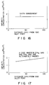
- Fig. 16 shows an example of the result of measurement of the phosphorus concentration in the polysilicon films after annealing the thus formed polysilicon films 73 1 to 73 4 and 75 1 to 75 4 at a high temperature. It is understood from Fig. 16 that the distribution of the phosphorus concentration of the polysilicon films is substantially uniform irrespective of the position of the semiconductor substrate in the low pressure CVD furnace. The reason for this can be explained as follows. That is, the phosphorus concentration of a polysilicon film formed when SiH 4 gas and PH 3 gas are alternately passed is distributed as shown in Fig. 17 according to the position of the semiconductor substrate in the low pressure CVD furnace and the phosphorus concentration tends to be higher as the distance from the gas inlet port is longer. The reason for this is not clear but may be considered to be because phosphorus adsorbed on the surface of the film after PH 3 gas supply is interrupted is removed when SiH 4 is passed again and PH 3 gas may be transferred to the downstream side of the gas flow.
- a step of forming a polysilicon film containing impurity when a polysilicon film containing impurity is formed on a semiconductor substrate, a step of forming a polysilicon film containing no impurity, a step of depositing a polysilicon film and at the same time doping desired impurity and a step of forming an impurity layer near the surface of the polysilicon film by passing gas containing desired impurity on and over the semiconductor substrate are combined in a desired order and the thus combined three steps are repeatedly effected to form the polysilicon film to a desired thickness.
- the deposition speed in the in-situ doping process of depositing a polysilicon film containing impurity by simultaneously introducing SiH 4 gas and PH 3 gas can be set less one half of the deposition speed in the process of depositing a polysilicon film by passing SiH 4 gas. Therefore, the total sum of time for the process of depositing the polysilicon film by passing SiH 4 gas and time for the process of forming a mono-layer of phosphorus on the surface of the polysilicon film by passing PH 3 gas may become substantially equal to time for the in-situ doping process of depositing the polysilicon film to the same thickness, and thus in the method of the sixth embodiment, a problem that the deposition time becomes long can be prevented.
- phosphorus is doped as impurity by use of PH 3 gas, but it is possible to use another dopant (for example, at least one of B, As, Sb, Al and Ga), and if B is used as the dopant, for example, B 2 H 6 gas may be used and if As is used as the dopant, for example, AsH 3 gas may be used.
- B is used as the dopant
- B 2 H 6 gas may be used
- As is used as the dopant
- AsH 3 gas may be used.
- SiH 4 gas is used to deposit the polysilicon film, but, for example, Si 2 H 6 gas may be used.
- the polysilicon film is deposited at the reaction temperature of 610°C, but it is also possible to dope impurity in the same manner as in each of the above embodiments in a case where the reaction temperature is set below 600°C and a silicon film other than a polysilicon film, for example, an amorphous silicon film is deposited.
- the deposition of the polysilicon film and impurity doping are effected under the pressure of 66.6 Pa to 133 Pa (0.5 Torr to 1 Torr), but it is also possible to effect the same under the lowered pressure of 0.13 Pa to 1.33.10 4 Pa (0.001 Torr to 100 Torr).
- the semiconductor device manufacturing method of this invention it is possible to manufacture a semiconductor device in which, when a polysilicon film containing impurity is formed on the semiconductor substrate in which at least part of the main surface is covered with the insulation film in the low pressure CVD device, the impurity concentration of the polysilicon film can be made uniform in the substrate surface area without using a special furnace structure and controlling the gas flow.
- the semiconductor device manufacturing method of this invention it is possible to manufacture a semiconductor device in which, when a polysilicon film containing impurity is formed on the semiconductor substrate in which at least part of the main surface is covered with the insulation film in the low pressure CVD device, the deposition speed of the polysilicon film and the impurity concentration of the polysilicon film can be prevented from becoming non-uniform depending on the position of the semiconductor substrate in the low pressure CVD furnace.
Description
- This invention relates to a semiconductor device manufacturing method according to the preamble of
claim 1. - Such a method is known from Journal of Applied Physics, vol. 65, no. 11, 1 June 1985, pp. 4435-4437, S.F. Gong el al., "A metal oxide silicon field effect transistor made by means of solid phase doping".
- In the conventional semiconductor device, an electrode or electrode wiring formed of a polysilicon film as a main component is formed on an insulation film on the main surface area of a semiconductor substrate (wafer), and an additional insulation film is often formed on the same. In this case, impurity such as phosphorus (P) is generally doped into the polysilicon film to lower the resistance thereof so that it can be used for a desired purpose. An example in which phosphorus is doped is explained here.
- In general, when a polysilicon film containing impurity is formed on the semiconductor substrate, a polysilicon film containing no impurity is first formed by deposition on the semiconductor substrate, the semiconductor substrate is heated to a temperature of higher than 600°C to thermally diffuse phosphorus while the surface of the polysilicon film is being oxidized, and then the oxide film on the surface of the polysilicon film is removed by use of chemical such as hydrofluoric acid.
- However, the above method has defects that variation in the concentration of phosphorus contained in the polysilicon film is large in the surface area of the substrate (in the surface area of the wafer) and it is difficult to increase the diameter of the semiconductor substrate and since the oxide film formed on the polysilicon film is removed by use of chemical after phosphorus is diffused, the chemical may damage the underground layer through the grain boundary of the polysilicon film when the polysilicon film is formed to be thinner with increasing miniaturization of the element.
- Further, in addition to the above method, there is a method of forming a polysilicon film containing no impurity on the semiconductor substrate and then doping phosphorus into the polysilicon film by use of ion-implantation.
- Further, in addition to the above method, an in-situ doping method of doping impurity at the same time as formation of the polysilicon film is proposed.
- Fig. 1 schematically shows a general construction of a low pressure CVD (chemical vapor deposition) device used when effecting the in-situ doping method. In Fig. 1, 91 denotes a low pressure CVD furnace, 92, 92, --- denote semiconductor substrates (wafers) disposed in the CVD furnace, 93 denotes a sample table (boat) for holding a group of semiconductor substrates in a horizontal position, 94 denotes a gas inlet port for permitting silane (SiH4) gas to be supplied into the CVD furnace via the lower portion thereof, 95 denotes a gas inlet port for permitting phosphine (PH3) gas to be supplied into the CVD furnace via the lower portion thereof, and 96 denotes an exhaust port provided on the upper portion of the CVD furnace.
- In the conventional in-situ doping method, SiH4 gas and PH3 gas are simultaneously introduced into the CVD furnace so as to form a polysilicon film by deposition and at the same time dope phosphorus.
- However, in the conventional in-situ doping method, uniformity of phosphorus concentration of the polysilicon film in the surface area of the substrate can be improved to some extent, it is necessary to use a special sample table on which the semiconductor substrates are mounted and pay special attention to the flow of gas, and in a case where an ordinary sample table is used, variation in the film thickness of the polysilicon film in the substrate surface area and variation in the phosphorus concentration in the polysilicon film will become large. Further, even when a special sample table is used, the deposition speed and phosphorus concentration may become non-uniform depending on the depositing position (distance from the gas inlet port) inside the CVD furnace.
- Fig. 2 shows an example of variation in the film thickness of the polysilicon film in the substrate surface area and variation in the phosphorus concentration of the polysilicon film in the substrate surface area.
- Fig. 3 shows an example of a condition wherein the deposition speed of the polysilicon film and the concentration of phosphorus in the polysilicon film become non-uniform depending on the position (distance from the gas inlet port) of the semiconductor substrate inside the low pressure CVD furnace, that is, the trend of variation in the properties of semiconductor substrates.
- This phenomenon is considered to occur because the attachment probability of semiconductor atoms (Si in this embodiment) when phosphorus is adsorbed on the surface is small so as to lower the deposition speed and the concentration distribution of phosphorus becomes non-uniform since the speed of decomposition of PH3 gas for supplying impurity and the speed of decomposition of SiH4 for depositing silicon are different to make the concentration distribution of phosphorus non-uniform. The deposition speed of the polysilicon film and the phosphorus concentration in the polysilicon film become non-uniform depending on the position of the semiconductor substrate inside the low pressure CVD furnace.
- Further, as described before, it is known that when the method of thermally diffusing phosphorus while oxidizing the surface of the polysilicon film is used, the withstanding voltage of a thermal oxide film to be formed on the polysilicon film largely depends on the phosphorus concentration. Since this is particularly important in elements having a laminated structure such as EPROMs (ultra violet erasable and programmable read only memories) or DRAMs (dynamic type random access memories) using memory cells of stack structure, it is necessary to suppress variation in the phosphorus concentration of the polysilicon film in the substrate surface area. Further, since the sheet resistance of the polysilicon in the substrate surface area and the process margin at the time of etching are also largely dependent on the phosphorus concentration, variation in the phosphorus concentration of the polysilicon film in the substrate surface area must be small. Fig. 4 shows an example of variation in the withstanding voltage of the thermal oxide film in the substrate surface area and variation in the phosphorus concentration of the polysilicon film in the substrate surface area.
- As described above, a method of manufacturing the conventional semiconductor device has problems that when a polysilicon film containing impurity is formed on a semiconductor substrate in which the entire portion or part of the main surface area is covered with an insulation film, variation in the impurity concentration of the polysilicon film in the substrate surface area becomes large so that the profile of the impurity concentration of the polysilicon film formed in a contact hole which is formed in part of an insulation film formed on the substrate or a trench which is formed in part of the substrate may become non-uniform in the depth direction thereof and variation in the withstanding voltage of an insulation film to be formed on the polysilicon film becomes large.
- Further, a method of manufacturing the semiconductor device including the conventional in-situ doping method has a problem that the deposition speed of a polysilicon film and the phosphorus concentration in the polysilicon film become non-uniform depending on the position of the semiconductor substrate inside the low pressure CVD furnace.
- An object of this invention is to provide a semiconductor device manufacturing method by which the impurity concentration of a polysilicon film containing impurity can be made uniform in the substrate surface area without using a special furnace structure or control of gas flow when the polysilicon film is formed on the semiconductor substrate whose main surface is at least partly covered with an insulation film in a low pressure CVD device.
- Another object of this invention is to provide a semiconductor device manufacturing method by which the deposition speed of a polysilicon film containing impurity or the impurity concentration of a polysilicon film can be prevented from being made non-uniform depending on the position of a semiconductor substrate inside a low pressure CVD furnace when the polysilicon film is formed on the semiconductor substrate whose main surface is at least partly covered with an insulation film in a low pressure CVD device.
- According to this invention, there is provided a semiconductor device manufacturing method of the initially defined type having the characterizing features of
claim 1. - Preferred embodiments are listed in the dependent claims.
- This invention can be more fully understood from the following detailed description when taken in conjunction with the accompanying drawings, in which:
- Fig. 1 is a view schematically showing a general construction of a low pressure CVD device used for effecting the in-situ doping process;
- Fig. 2 is a characteristic diagram showing an example of variation in the film thickness of a polysilicon film formed by use of the conventional in-situ doping method in the substrate surface area and variation in the phosphorus concentration of a polysilicon film in the substrate surface area;
- Fig. 3 is a characteristic diagram showing an example of a trend that the deposition speed of a polysilicon film formed by use of the conventional in-situ doping method and the phosphorus concentration of the polysilicon film become non-uniform depending on the position of the semiconductor substrate in the low pressure CVD furnace;
- Fig. 4 is a characteristic diagram showing an example of variation in the withstanding voltage of a thermal oxide film lying in the substrate surface area and disposed on a polysilicon film which is formed by use of the conventional thermally diffusing method and variation in the phosphorus concentration of the polysilicon film in the substrate surface area;
- Fig. 5 is a cross sectional view showing an example of the structure of a capacitor formed by use of a first embodiment of a semiconductor device manufacturing method according to this invention;
- Figs. 6A to 6G are cross sectional views showing element structures in respective steps of the manufacturing method of the first embodiment;
- Fig. 7 is a characteristic diagram showing an example of the result of measurement of variation in the film thickness of a first polysilicon film of the capacitor shown in Fig. 5 in the substrate surface area and variation in the phosphorus concentration of the first polysilicon film in the substrate surface area;
- Fig. 8 is a characteristic diagram showing an example of the result of measurement and comparison of a holding voltage of a capacitor shown in Fig. 5 and that of a capacitor formed by the conventional method;
- Fig. 9 is a cross sectional view showing an example of the structure of a second embodiment of a semiconductor device according to this invention;
- Fig. 10 is a diagram showing an impurity profile of a polysilicon film of the device showing in Fig. 9;
- Figs. 11A to 11F are cross sectional views showing element structures in respective steps of the manufacturing method of a third embodiment of this invention;
- Figs. 12A to 12F are cross sectional views showing element structures in respective steps of the manufacturing method of a fourth embodiment of this invention;
- Fig. 13 is a characteristic diagram showing an example of the result of measurement of the electrical resistance of a polysilicon laminated film shown in Fig. 12;
- Figs. 14A to 14D are cross sectional views showing element structures in respective steps of the manufacturing method of a fifth embodiment of this invention;
- Figs. 15A to 15E are cross sectional views showing element structures in respective steps of the manufacturing method of a sixth embodiment of this invention;
- Fig. 16 is a characteristic diagram showing an example of the result of measurement of the phosphorus concentration of the polysilicon film formed by use of the method according to the sixth embodiment; and
- Fig. 17 is a diagram showing an example of a condition in which the phosphorus concentration of a polysilicon film formed when SiH4 gas and PH3 gas are alternately passed in the fifth embodiment distributes depending on the position of the semiconductor substrate in a low pressure CVD furnace.
- There will now be described an embodiment of this invention with reference to the accompanying drawings.
- Fig. 5 shows an example of the structure of a capacitor formed on the main surface of a semiconductor substrate. In the drawing, 11 denotes a silicon substrate, 12 denotes a first insulation film, 17 denotes a first polysilicon film used as one of the electrodes of the capacitor, 16 denotes a second insulation film serving as a dielectric layer of the capacitor and 18 denotes a second polysilicon serving as the other electrode of the capacitor.
- In the above capacitor, for example, phosphorus is contained as impurity in the
first polysilicon film 17 serving as one of the electrodes. The impurity concentration in the depth direction of thefirst polysilicon film 17 is made uniform. - Next, an example of a method of manufacturing the capacitor of the above construction is explained.
- First, as shown in Fig. 6A, the first insulation film (thermal oxide film) 12 with a film thickness of 50 nm (500Å) is formed on the entire portion of the main surface of the
silicon substrate 11. Next, as shown in Fig. 6B, the silicon substrate is disposed in a horizontal position in a low pressure CVD device as shown in Fig. 1, the reaction temperature is set at 610°C and air is exhausted from the upper portion by means of a vacuum pump. The pressure at this time can be set in a range of 0.13 Pa to 1.33.104 Pa (0.001 Torr to 100 Torr) and in this embodiment, the pressure is set at 66.6 Pa (0.5 Torr), and apolysilicon film 13 containing no impurity is formed to a thickness of at least 10 nm (100Å) on thefirst insulation film 12 by introducing SiH4 gas from the lower portion and thermally decomposing the same on and over thefirst insulation film 12. In this case, it is necessary to cover the surface of thefirst insulation film 12 with thepolysilicon film 13 of uniform surface density and it is desirable to set the thickness of thepolysilicon film 13 to at least approx. 10 nm (100Å). - Next, PH3 gas is passed under the reaction pressure of 66.6 Pa (0.5 Torr) and thermally decomposed on and over the
polysilicon film 13 to adsorb and diffuse phosphorus on and near the surface of the polysilicon film so as to form a mono-layer 14 of phosphorus as shown in Fig. 6C after the above step, that is, without exposing the ( substrate to the outside air. - Then, SiH4 gas is thermally decomposed on and over the
polysilicon film 13 at the reaction temperature of 610°C to deposit apolysilicon film 15 as shown in Fig. 6D after the above step, that is, without exposing the substrate to the outside air. - Next, as shown in Fig. 6E, the
polysilicon film 15 is thermally oxidized at a temperature of approx. 1000°C to form the second insulation film (thermal oxide film) 16 with a thickness of approx. 30 nm (300Å) on the surface thereof. Thesecond insulation film 16 serves as the dielectric layer of the capacitor. Further, phosphorus of the mono-layer 14 is diffused into thepolysilicon films polysilicon films first polysilicon film 17. Thefirst polysilicon film 17 serves as one of the electrodes of the capacitor. In this case, the thickness of thefirst polysilicon film 17 is 20 nm (200Å) and the average concentration of phosphorus in thefirst polysilicon film 17 is 5 × 1020 cm-3. - Next, as shown in Fig. 6F, the
second polysilicon film 18 having a thickness of approx. 350 nm (3500Å) and surface resistance of approx. 20Ω and serving as the other electrode of the capacitor is formed on thesecond insulation film 16. - Next, the
second polysilicon film 18,second insulation film 16 andfirst polysilicon film 17 are selectively etched by the photoetching process to form the capacitor as shown in Fig. 6G. - Fig. 7 shows an example of the result of measurement of variation in the film thickness of the first polysilicon film of the capacitor formed in the above-described manner in the substrate surface area and variation in the phosphorus concentration of the
first polysilicon film 17 in the substrate surface area. It is understood from Fig. 7 that the above variations are significantly improved in comparison with those for a polysilicon film formed by the in-situ doping method in which SiH4 gas and PH3 gas are simultaneously introduced. - Fig. 8 shows an example of the result of measurement and comparison of a holding voltage of a capacitor formed in the above-described manner and that of a capacitor formed by the conventional method. In this case, the ordinate indicates the withstanding voltage of the
second insulation film 16 by the intensity of electric field when a voltage is applied between thefirst polysilicon film 17 and thesecond polysilicon film 18 and the abscissa indicates the position in the substrate surface area. - It is clearly understood from Fig. 8 that the withstanding voltage of the capacitor formed by use of the method of the above embodiment is improved in comparison with the withstanding voltage of the capacitor formed by the conventional method.
- Fig. 9 is a sectional view showing a semiconductor device according to a second embodiment of the invention. Many of the components of this device are identical to those of the device shown in Fig. 5, and will therefore be designated at the same numerals as those used in Fig. 5 and will not be described in detail.
- In the second embodiment (Fig. 9), a
trench 19 is formed in asilicon substrate 11. Thetrench 19 has a rectangular cross section, and its both sides extend vertically. Afirst insulation film 12 is formed in thistrench 19. Apolysilicon film 17 is formed on theinsulation film 12 and, hence, in thetrench 19, and also on the surface of thesilicon substrate 11. Thepolysilicon film 17 also contains an impurity such as phosphorus. - The
polysilicon film 17, which is formed partly in thetrench 19 and partly on thesubstrate 11 as is shown in Fig. 9, is formed in the same method as in the first embodiment (Fig. 5). As shown in Fig. 10, thefilm 17 has an impurity concentration (i.e., phosphorus concentration) which is uniform in the depth direction. - In the first embodiment, the first step of forming the
first polysilicon film 13 containing no impurity on the semiconductor substrate in which at least part of the main surface is covered with the insulation film is effected, then the second step of forming the impurity layer on the surface of thepolysilicon film 13 by passing gas containing desired impurity on and over the semiconductor substrate is effected, and the first step is repeatedly effected. However, if required, it is possible to form thepolysilicon film 17 to a desired thickness by repeatedly effecting the first and second steps by a desired number of times. Figs. 11A to 11F show respective steps of a method including the above steps and according to a third embodiment of this invention. That is, as shown in Fig. 11A, afirst insulation film 12 with a thickness of 50 nm (500Å) is formed on the entire portion of the main surface of asilicon substrate 11 in the same manner as in a case shown in Fig. 6A. - Next, as shown in Fig. 11B, the silicon substrate is placed in a horizontal position in a low pressure CVD device and a
polysilicon film 13 containing no impurity is deposited on thefirst insulation film 12 in the same manner as in a case shown in Fig. 6B. - Next, as shown in Fig. 11C, PH3 gas is passed under the reaction pressure of 66.6 Pa (0.5 Torr) and thermally decomposed on and over the
polysilicon film 13 to adsorb and diffuse phosphorus on and near the surface portion of the polysilicon film so as to form a first mono-layer 141 of phosphorus after the above step, that is, without exposing the substrate to the outside air. Then, SiH4 gas is thermally decomposed on and over thepolysilicon film 13 at the reaction temperature of 610°C to deposit apolysilicon film 151 without exposing the substrate to the outside air. - After this, as shown in Fig. 11D, a second mono-
layer 142 is formed on thepolysilicon film 151 in the same manner as described above and then apolysilicon film 152 is deposited on the mono-layer. - Next, as shown in Fig. 11E, the
polysilicon film 152 is thermally oxidized at a temperature of approx. 1000°C to form a second insulation film (thermal oxide film) 16 with a thickness of approx. 30 nm (300Å) on the surface thereof. Thesecond insulation film 16 serves as the dielectric layer of the capacitor. Further, phosphorus of the first and second mono-layers polysilicon films polysilicon films second polysilicon film 18 having a thickness of approx. 350 nm (3500Å) and surface resistance of approx. 20Ω and serving as the other electrode of the capacitor is formed on the first polysilicon film 17'. - Next, the
second polysilicon film 18,second insulation film 16 and first polysilicon film 17' are sequentially and selectively etched by the photoetching process to form the capacitor as shown in Fig. 11F. - In the method of the above embodiment, the thicknesses of the
polysilicon films original polysilicon films - In the methods of the first and third embodiments, the
polysilicon film 17 or 17' is formed on the silicon substrate in which the entire portion of the main surface is covered with thefirst insulation film 12. Next, an example of a method of forming a polysilicon film on a semiconductor substrate having an impurity region formed in the substrate surface area under an opening which is formed in the first insulation film is explained as a fourth embodiment with reference to Figs. 12A to 12F. - First, as shown in Fig. 12A, a first insulation film (thermal oxide film) 42 is formed to a thickness of 50 nm (500Å) on the entire portion of the main surface of a P--
type silicon substrate 41. Then, As ions are ion-implanted into thesilicon substrate 41 through thefirst insulation film 42 and heat treatment is effected to diffuse the As ions so as to form an N+-type region 43 in part of thesilicon substrate 41. - Next, as shown in Fig. 12B, a
contact hole 44 is formed in thefirst insulation film 42 on the N+-type region 43 and then SiH4 gas is thermally decomposed on and over theinsulation film 42 at the reaction temperature of 610°C and under the reaction pressure of 66.6 Pa (0.5 Torr) in the low pressure CVD device to deposit apolysilicon film 45 containing no impurity on thefirst insulation film 42 and in thecontact hole 44. - After this, as shown in Fig. 12C, PH3 gas is thermally decomposed on and over the
polysilicon film 45 under the reaction pressure of 66.6 Pa (0.5 Torr) in the low pressure CVD device to form a mono-layer 46 of phosphorus on the surface of the polysilicon film. - Then, SiH4 gas is thermally decomposed on and over the
insulation film 45 at the reaction temperature of 610°C in the low pressure CVD device to deposit apolysilicon film 47 as shown in Fig. 12D. - Next, as shown in Fig. 12E, a passivation film (for example, a phosphorus-silicate-glass film : PSG film) 48 is formed on the entire surface of the substrate. Further, phosphorus contained in the mono-
layer 46 of phosphorus is diffused into thepolysilicon films passivation film 48 is formed and a later melting step is effected, thereby integrating thepolysilicon films polysilicon film 49. Thepolysilicon film 49 serves as an electrode lead-out wiring extending from the N+-type region 43. - Next, as shown in Fig. 12F, the
passivation film 48 is selectively etched to form a contact hole, and then an aluminum-silicon film is formed on the entire surface of the substrate and patterned to form anelectrode 50. - Fig. 13 shows an example of the result of measurement of electrical resistance of the
polysilicon film 49 of the element formed in the above-described manner. As is clearly understood from Fig. 12, variation in the electrical resistance in the substrate surface area is smaller in the case of thepolysilicon film 49 formed by the method of the fourth embodiment than in the case of the polysilicon film formed by the conventional method and a proper electrical characteristic can be attained. This is considered to be because phosphorus is uniformly doped in thepolysilicon film 49. - A method according to a fifth embodiment of this invention is explained. The method of this embodiment is to form a polysilicon film containing impurity on a semiconductor substrate in which part of the main surface is covered with an insulation film and the other portion is exposed to a conductive layer.
- First, a semiconductor structure shown in Fig. 14A is formed. In Fig. 14A, 61 denotes a P--type silicon substrate, 62 a first insulation film, 63 an N+-type region, 64 a polysilicon film containing impurity, 65 a conductive film formed of, for example, MoSi, and 66 a second insulation film. The
polysilicon film 64 is formed by the same method as that for forming thepolysilicon film 49 in the fourth embodiment. - Next, as shown in Fig. 14B, part of a
second insulation film 66 is etched to form a via-hole and then SiH4 gas is thermally decomposed on and over thesecond insulation film 66 at the reaction temperature of 610°C and under the reaction pressure of 66.6 Pa (0.5 Torr) in the low pressure CVD device to deposit apolysilicon film 67 containing no impurity on thesecond insulation film 66. After this, PH3 gas is thermally decomposed on and over thepolysilicon film 67 under the reaction pressure of 66.6 Pa (0.5 Torr) in the low pressure CVD device to form a mono-layer 68 of phosphorus on the surface of the polysilicon film. - Then, SiH4 gas is thermally decomposed on and over the
polysilicon film 68 at the reaction temperature of 610°C in the low pressure CVD device to deposit apolysilicon film 69 as shown in Fig. 14C. - After this, the semiconductor structure is subjected to the annealing process at a high temperature to diffuse phosphorus of the mono-
layer 68 into thepolysilicon films polysilicon films polysilicon film 70. Thepolysilicon film 70 serves as a lead-out wiring of theconductive film 65 formed of MoSi. - The
conductive film 65 may be formed of at least one of semiconductor, metal, metal silicate and metal nitride instead of MoSi. - Next, a method according to a sixth embodiment of this invention is explained.
- That is, as shown in Fig. 15A, a first insulation film (thermal oxide film) 72 is formed to a thickness of 50 nm (500Å) on the entire portion of the main surface of a
silicon substrate 71. - Next, as shown in Fig. 15B, the silicon substrate is placed in a horizontal position in the low pressure CVD device and polysilicon film 731 is formed on
first insulation film 72 and then, as shown in Fig. 15C. PH3 gas of 10 sccm is passed under a condition that the reaction temperature is set at 610°C and the reaction pressure is set at 133.3 Pa (1 Torr) and is thermally decomposed on and over the polysilicon film 731 so as to form a mono-layer 741 of phosphorus on the surface of the polysilicon film 731. After PH3 gas is passed for 10 minutes, supply of PH3 gas is interrupted. - Then, SiH4 gas of 10 sccm is passed under a condition of the reaction temperature of 610°C and the reaction pressure of 66.6 Pa (0.5 Torr) so as to form a polysilicon film 751 to a thickness of 50 nm (500Å) on the mono-
layer 741 as shown in Fig. 14D after the above step, that is, without exposing the substrate to the outside air. - After this, the three steps shown in Figs. 15B, 15C and 15D are repeatedly effected by three times to form a polysilicon film 732, a mono-
layer 742 of phosphorus, a polysilicon film 752, a polysilicon film 733, a mono-layer 743 of phosphorus, a polysilicon film 753, a polysilicon film 734, a mono-layer 744 of phosphorus, and a polysilicon film 754 as shown in Fig. 15E. In this case, the film thicknesses of the polysilicon films are so determined as to set the total thickness of the polysilicon films 731 to 734 and 751 to 754 to approx. 300 nm (3000Å) if the thickness of each of the mono-layers 741 to 744 is neglected. - Fig. 16 shows an example of the result of measurement of the phosphorus concentration in the polysilicon films after annealing the thus formed polysilicon films 731 to 734 and 751 to 754 at a high temperature. It is understood from Fig. 16 that the distribution of the phosphorus concentration of the polysilicon films is substantially uniform irrespective of the position of the semiconductor substrate in the low pressure CVD furnace. The reason for this can be explained as follows. That is, the phosphorus concentration of a polysilicon film formed when SiH4 gas and PH3 gas are alternately passed is distributed as shown in Fig. 17 according to the position of the semiconductor substrate in the low pressure CVD furnace and the phosphorus concentration tends to be higher as the distance from the gas inlet port is longer. The reason for this is not clear but may be considered to be because phosphorus adsorbed on the surface of the film after PH3 gas supply is interrupted is removed when SiH4 is passed again and PH3 gas may be transferred to the downstream side of the gas flow.
- In the method of the sixth embodiment, when a polysilicon film containing impurity is formed on a semiconductor substrate, a step of forming a polysilicon film containing no impurity, a step of depositing a polysilicon film and at the same time doping desired impurity and a step of forming an impurity layer near the surface of the polysilicon film by passing gas containing desired impurity on and over the semiconductor substrate are combined in a desired order and the thus combined three steps are repeatedly effected to form the polysilicon film to a desired thickness.
- Therefore, it becomes possible to improve the uniformity of the phosphorus concentration and the uniformity of the film thickness by obtaining a proper film thickness by combining a method of depositing a polysilicon film by separately introducing SiH4 gas and PH3 gas and the in-situ doping method of depositing a polysilicon film by simultaneously introducing SiH4 gas and PH3 gas as in the conventional method.
- The deposition speed in the in-situ doping process of depositing a polysilicon film containing impurity by simultaneously introducing SiH4 gas and PH3 gas can be set less one half of the deposition speed in the process of depositing a polysilicon film by passing SiH4 gas. Therefore, the total sum of time for the process of depositing the polysilicon film by passing SiH4 gas and time for the process of forming a mono-layer of phosphorus on the surface of the polysilicon film by passing PH3 gas may become substantially equal to time for the in-situ doping process of depositing the polysilicon film to the same thickness, and thus in the method of the sixth embodiment, a problem that the deposition time becomes long can be prevented.
- In the method of each of the above embodiments, phosphorus is doped as impurity by use of PH3 gas, but it is possible to use another dopant (for example, at least one of B, As, Sb, Aℓ and Ga), and if B is used as the dopant, for example, B2H6 gas may be used and if As is used as the dopant, for example, AsH3 gas may be used.
- In the method of each of the above embodiments, SiH4 gas is used to deposit the polysilicon film, but, for example, Si2H6 gas may be used.
- In the method of each of the above embodiments, the polysilicon film is deposited at the reaction temperature of 610°C, but it is also possible to dope impurity in the same manner as in each of the above embodiments in a case where the reaction temperature is set below 600°C and a silicon film other than a polysilicon film, for example, an amorphous silicon film is deposited.
- Further, in the method of each of the above embodiments, the deposition of the polysilicon film and impurity doping are effected under the pressure of 66.6 Pa to 133 Pa (0.5 Torr to 1 Torr), but it is also possible to effect the same under the lowered pressure of 0.13 Pa to 1.33.104 Pa (0.001 Torr to 100 Torr).
- As described above, when using the semiconductor device manufacturing method of the invention, it is possible to manufacture a semiconductor device in which variation in impurity concentration of the polysilicon film formed on the semiconductor substrate in which at least part of the main surface is covered with the insulation film can be improved.
- Further, when using the semiconductor device manufacturing method of this invention, it is possible to manufacture a semiconductor device in which, when a polysilicon film containing impurity is formed on the semiconductor substrate in which at least part of the main surface is covered with the insulation film in the low pressure CVD device, the impurity concentration of the polysilicon film can be made uniform in the substrate surface area without using a special furnace structure and controlling the gas flow.
- Further, when using the semiconductor device manufacturing method of this invention, it is possible to manufacture a semiconductor device in which, when a polysilicon film containing impurity is formed on the semiconductor substrate in which at least part of the main surface is covered with the insulation film in the low pressure CVD device, the deposition speed of the polysilicon film and the impurity concentration of the polysilicon film can be prevented from becoming non-uniform depending on the position of the semiconductor substrate in the low pressure CVD furnace.
Claims (14)
- A semiconductor device manufacturing method comprising:- a first step of covering at least part of the main surface area of a semiconductor substrate (11; 41; 71) with a first insulation film (12; 42; 72);- a second step of forming a first non-single crystal silicon film (13; 45; 731) on the entire surface;characterized by- a third step of passing a gas containing a desired impurity on said semiconductor substrate to form an impurity monolayer (14; 46; 741) on the surface of said first non-single crystal silicon film;- a fourth step of forming a second non-single crystal silicon film (15; 47; 751) containing no impurity after said third step, said second non-single crystal silicon film (15; 47; 751) being formed on said impurity monolayer;- a fifth step of diffusing impurity from said impurity monolayer into said first and second non-single crystal silicon films after said fourth step thereby forming a polysilicon layer with a uniform impurity concentration- an LPCVD apparatus being used for forming each of the non-single crystal silicon films (13; 45, 731, 15, 47, 751) and the impurity monolayer (14; 46; 741); and- the successive formation of the first non-single crystal silicon film (13; 45; 731), the second non-single crystal silicon film (15, 47, 751) and the impurity monolayer (14; 46; 741) being carried out without exposing the substrate to the outside air.
- A method according to claim 1, characterized in that said first non-single crystal silicon film (13; 45; 731) contains no impurity.
- A semiconductor device manufacturing method according to claim 1 or 2, characterized in that said first non-single crystal silicon film (13; 45; 731) is a polysilicon film.
- A device manufacturing method according to claim 1 or 2, characterized in that said second non-single crystal silicon film (15; 47; 751) is a polysilicon film.
- A device manufacturing method according to claim 1 or 2, characterized in that said fifth step is effected at the same time as a step of forming a second insulation film (16; 48) on the surface of said second non-single crystal silicon film (15; 47; 751) by the thermal oxidation process.
- A semiconductor device manufacturing method according to claim 1 or 2, characterized by further comprising a sixth step of repeatedly effecting a combination of said third and fourth steps by a plurality of times after said fourth step and before said fifth step.
- A device manufacturing method according to claim 1, characterized in that said impurity monolayer (14; 46; 741) contains at least one selected from a group consisting of P, B, As, Sb, Aℓ and Ga.
- A device manufacturing method according to claim 1 or 2, characterized in that the film thickness of said first and second non-single crystal silicon films (13; 45; 731) are determined such that the average impurity concentration of said first and second non-single crystal silicon (15; 47; 751) films after said impurity is diffused are set to desired values.
- A semiconductor device manufacturing method according to claim 1, characterized by doping a desired impurity into said first non-single crystal silicon film (13; 45; 731) at the same time as forming the first non-single crystal silicon film (13; 45; 731).
- A device manufacturing method according to claim 9, characterized in that the film thicknesses of said first and second non-single crystal silicon films (13; 45; 731; 15; 47; 751) are determined such that the average impurity concentration of said first and second non-single crystal silicon (13; 45; 731; 15; 47; 751) films after said impurity is diffused are set to desired values.
- A device manufacturing method according to claim 2 or 9, characterized in that said second to fourth steps are repeatedly effected by a desired number of times to set the total thickness of said non-single crystal silicon film to a desired thickness.
- A device manufacturing method according to claim 9, characterized in that said impurity monolayer contains at least one selected from a group consisting of P, B, As, Sb, Aℓ and Ga.
- A method according to any of claims 1 to 5, characterized in that an opening (44) which reaches the surface of said semiconductor substrate (11; 41; 71) is formed in said first insulation film (42) and said first non-single crystal silicon film (45) is also formed in said opening (44).
- A method according to claim 1 or 2, characterized in that said first non-single crystal silicon film (13; 45; 731) is an amorphous silicon film.
Applications Claiming Priority (2)
| Application Number | Priority Date | Filing Date | Title |
|---|---|---|---|
| JP2105299A JP2558917B2 (en) | 1990-04-23 | 1990-04-23 | Method for manufacturing semiconductor device |
| JP105299/90 | 1990-04-23 |
Publications (3)
| Publication Number | Publication Date |
|---|---|
| EP0454055A2 EP0454055A2 (en) | 1991-10-30 |
| EP0454055A3 EP0454055A3 (en) | 1993-05-05 |
| EP0454055B1 true EP0454055B1 (en) | 1996-11-27 |
Family
ID=14403816
Family Applications (1)
| Application Number | Title | Priority Date | Filing Date |
|---|---|---|---|
| EP91106512A Expired - Lifetime EP0454055B1 (en) | 1990-04-23 | 1991-04-23 | Semiconductor device and method for manufacturing the same |
Country Status (4)
| Country | Link |
|---|---|
| EP (1) | EP0454055B1 (en) |
| JP (1) | JP2558917B2 (en) |
| KR (1) | KR960016220B1 (en) |
| DE (1) | DE69123282T2 (en) |
Families Citing this family (1)
| Publication number | Priority date | Publication date | Assignee | Title |
|---|---|---|---|---|
| EP0505877A2 (en) * | 1991-03-27 | 1992-09-30 | Seiko Instruments Inc. | Impurity doping method with adsorbed diffusion source |
Family Cites Families (13)
| Publication number | Priority date | Publication date | Assignee | Title |
|---|---|---|---|---|
| JPS529512B2 (en) * | 1972-11-14 | 1977-03-16 | ||
| JPS5138870A (en) * | 1974-09-27 | 1976-03-31 | Sharp Kk | HANDOTAISEIZOSOCHI |
| JPS606108B2 (en) * | 1976-07-07 | 1985-02-15 | 株式会社東芝 | Manufacturing method of semiconductor device |
| JPS59138332A (en) * | 1983-01-28 | 1984-08-08 | Seiko Instr & Electronics Ltd | Manufacture of semiconductor device |
| JPS615526A (en) * | 1984-06-20 | 1986-01-11 | Hitachi Ltd | Treating device |
| JPH07101677B2 (en) * | 1985-12-02 | 1995-11-01 | 株式会社東芝 | Method for manufacturing semiconductor device |
| JPS63153860A (en) * | 1986-12-17 | 1988-06-27 | Fujitsu Ltd | Manufacture of semiconductor device |
| JPS63182838A (en) * | 1987-01-26 | 1988-07-28 | Seiko Instr & Electronics Ltd | Manufacture of semiconductor device |
| JPS6422026A (en) * | 1987-07-17 | 1989-01-25 | Sony Corp | Manufacture of semiconductor device |
| JP2502109B2 (en) * | 1987-12-25 | 1996-05-29 | 三菱マテリアル株式会社 | Impurity diffusion method |
| JPH0234917A (en) * | 1988-07-25 | 1990-02-05 | Kokusai Electric Co Ltd | Method of forming polysilicon film doped with phosphorus in low concentration |
| EP0410390A3 (en) * | 1989-07-27 | 1993-02-24 | Seiko Instruments Inc. | Method of producing semiconductor device |
| EP0430166A3 (en) * | 1989-12-01 | 1993-05-12 | Seiko Instruments Inc. | Method of doping impurity into semiconductor films and patterned semiconductor strip |
-
1990
- 1990-04-23 JP JP2105299A patent/JP2558917B2/en not_active Expired - Lifetime
-
1991
- 1991-04-23 DE DE69123282T patent/DE69123282T2/en not_active Expired - Fee Related
- 1991-04-23 KR KR1019910006566A patent/KR960016220B1/en not_active IP Right Cessation
- 1991-04-23 EP EP91106512A patent/EP0454055B1/en not_active Expired - Lifetime
Also Published As
| Publication number | Publication date |
|---|---|
| DE69123282T2 (en) | 1997-04-30 |
| JPH045824A (en) | 1992-01-09 |
| EP0454055A2 (en) | 1991-10-30 |
| KR960016220B1 (en) | 1996-12-07 |
| DE69123282D1 (en) | 1997-01-09 |
| EP0454055A3 (en) | 1993-05-05 |
| JP2558917B2 (en) | 1996-11-27 |
| KR910019124A (en) | 1991-11-30 |
Similar Documents
| Publication | Publication Date | Title |
|---|---|---|
| KR100207444B1 (en) | Capacitor fabrication method and its device having high dielectronic layer and electrode | |
| US5733816A (en) | Method for depositing a tungsten layer on silicon | |
| US4931897A (en) | Method of manufacturing semiconductor capacitive element | |
| JP2761685B2 (en) | Method for manufacturing semiconductor device | |
| US6191443B1 (en) | Capacitors, methods of forming capacitors, and DRAM memory cells | |
| US5244835A (en) | Method of making contact electrodes of polysilicon in semiconductor device | |
| KR100191685B1 (en) | Process of fabricating capacitor having waved rough surface of accumulating electrode | |
| JPH11150249A (en) | Forming method of uneven polysilicon layer and substrate treatment device used by the same and semiconductor memory device | |
| US6153507A (en) | Method of fabricating semiconductor device providing effective resistance against metal layer oxidation and diffusion | |
| KR100202975B1 (en) | Fabrication method of semiconductor device | |
| US5413943A (en) | Semiconductor device and method of manufacturing the same | |
| EP0860863B1 (en) | A method for forming a laminated structure of polysilicon and tungsten silicide | |
| EP0454055B1 (en) | Semiconductor device and method for manufacturing the same | |
| EP0287031B1 (en) | High breakdown voltage insulating film provided between polysilicon layers | |
| GB2199987A (en) | Doped polycrystalline silicon layers for semiconductor devices | |
| JP3247242B2 (en) | Method for manufacturing semiconductor device | |
| US20050130418A1 (en) | Semiconductor device and manufacturing method therefor | |
| JPH1022467A (en) | Semiconductor device and manufacture thereof | |
| JPH08316474A (en) | Manufacture of semiconductor device | |
| US6403455B1 (en) | Methods of fabricating a memory device | |
| US20030003656A1 (en) | Method of manufacturing flash memory device | |
| JPH10125617A (en) | Method of manufacturing semiconductor device | |
| KR100296960B1 (en) | Method for forming polysilicon layer of semiconductor device | |
| KR100504434B1 (en) | Method of forming capacitor | |
| KR100200306B1 (en) | Polysilicon layer manufacturing method |
Legal Events
| Date | Code | Title | Description |
|---|---|---|---|
| PUAI | Public reference made under article 153(3) epc to a published international application that has entered the european phase |
Free format text: ORIGINAL CODE: 0009012 |
|
| 17P | Request for examination filed |
Effective date: 19910423 |
|
| AK | Designated contracting states |
Kind code of ref document: A2 Designated state(s): DE FR GB |
|
| PUAL | Search report despatched |
Free format text: ORIGINAL CODE: 0009013 |
|
| AK | Designated contracting states |
Kind code of ref document: A3 Designated state(s): DE FR GB |
|
| 17Q | First examination report despatched |
Effective date: 19931209 |
|
| GRAG | Despatch of communication of intention to grant |
Free format text: ORIGINAL CODE: EPIDOS AGRA |
|
| GRAH | Despatch of communication of intention to grant a patent |
Free format text: ORIGINAL CODE: EPIDOS IGRA |
|
| GRAH | Despatch of communication of intention to grant a patent |
Free format text: ORIGINAL CODE: EPIDOS IGRA |
|
| GRAA | (expected) grant |
Free format text: ORIGINAL CODE: 0009210 |
|
| AK | Designated contracting states |
Kind code of ref document: B1 Designated state(s): DE FR GB |
|
| REF | Corresponds to: |
Ref document number: 69123282 Country of ref document: DE Date of ref document: 19970109 |
|
| ET | Fr: translation filed | ||
| PGFP | Annual fee paid to national office [announced via postgrant information from national office to epo] |
Ref country code: FR Payment date: 19970409 Year of fee payment: 7 |
|
| PGFP | Annual fee paid to national office [announced via postgrant information from national office to epo] |
Ref country code: DE Payment date: 19970505 Year of fee payment: 7 |
|
| PLBE | No opposition filed within time limit |
Free format text: ORIGINAL CODE: 0009261 |
|
| STAA | Information on the status of an ep patent application or granted ep patent |
Free format text: STATUS: NO OPPOSITION FILED WITHIN TIME LIMIT |
|
| 26N | No opposition filed | ||
| PG25 | Lapsed in a contracting state [announced via postgrant information from national office to epo] |
Ref country code: FR Free format text: THE PATENT HAS BEEN ANNULLED BY A DECISION OF A NATIONAL AUTHORITY Effective date: 19980430 |
|
| PG25 | Lapsed in a contracting state [announced via postgrant information from national office to epo] |
Ref country code: DE Free format text: LAPSE BECAUSE OF NON-PAYMENT OF DUE FEES Effective date: 19990202 |
|
| REG | Reference to a national code |
Ref country code: FR Ref legal event code: ST |
|
| REG | Reference to a national code |
Ref country code: GB Ref legal event code: IF02 |
|
| PGFP | Annual fee paid to national office [announced via postgrant information from national office to epo] |
Ref country code: GB Payment date: 20100325 Year of fee payment: 20 |
|
| REG | Reference to a national code |
Ref country code: GB Ref legal event code: PE20 Expiry date: 20110422 |
|
| PG25 | Lapsed in a contracting state [announced via postgrant information from national office to epo] |
Ref country code: GB Free format text: LAPSE BECAUSE OF EXPIRATION OF PROTECTION Effective date: 20110422 |