EP0453530B1 - Festkörper-bildsensor - Google Patents
Festkörper-bildsensor Download PDFInfo
- Publication number
- EP0453530B1 EP0453530B1 EP90915584A EP90915584A EP0453530B1 EP 0453530 B1 EP0453530 B1 EP 0453530B1 EP 90915584 A EP90915584 A EP 90915584A EP 90915584 A EP90915584 A EP 90915584A EP 0453530 B1 EP0453530 B1 EP 0453530B1
- Authority
- EP
- European Patent Office
- Prior art keywords
- photodetectors
- photodetector
- adjacent
- region
- image sensor
- Prior art date
- Legal status (The legal status is an assumption and is not a legal conclusion. Google has not performed a legal analysis and makes no representation as to the accuracy of the status listed.)
- Expired - Lifetime
Links
- 239000002800 charge carrier Substances 0.000 claims abstract description 23
- 239000000758 substrate Substances 0.000 claims abstract description 23
- 230000004888 barrier function Effects 0.000 claims abstract description 15
- 239000000463 material Substances 0.000 claims abstract description 4
- 239000004065 semiconductor Substances 0.000 claims abstract description 4
- 238000005036 potential barrier Methods 0.000 claims description 10
- VYPSYNLAJGMNEJ-UHFFFAOYSA-N Silicium dioxide Chemical compound O=[Si]=O VYPSYNLAJGMNEJ-UHFFFAOYSA-N 0.000 description 14
- 235000012239 silicon dioxide Nutrition 0.000 description 7
- 239000000377 silicon dioxide Substances 0.000 description 7
- 239000012535 impurity Substances 0.000 description 5
- 230000010354 integration Effects 0.000 description 4
- 238000009416 shuttering Methods 0.000 description 3
- 238000009825 accumulation Methods 0.000 description 2
- 239000000969 carrier Substances 0.000 description 2
- 238000010586 diagram Methods 0.000 description 2
- 239000011810 insulating material Substances 0.000 description 2
- 239000002184 metal Substances 0.000 description 2
- 238000000034 method Methods 0.000 description 2
- 230000002411 adverse Effects 0.000 description 1
- 239000004020 conductor Substances 0.000 description 1
- 238000007796 conventional method Methods 0.000 description 1
- 229910021419 crystalline silicon Inorganic materials 0.000 description 1
- 230000009977 dual effect Effects 0.000 description 1
- 230000000694 effects Effects 0.000 description 1
- 239000007943 implant Substances 0.000 description 1
- 238000004519 manufacturing process Methods 0.000 description 1
- 229910021420 polycrystalline silicon Inorganic materials 0.000 description 1
- 239000007787 solid Substances 0.000 description 1
Images

Classifications
-
- H—ELECTRICITY
- H10—SEMICONDUCTOR DEVICES; ELECTRIC SOLID-STATE DEVICES NOT OTHERWISE PROVIDED FOR
- H10F—INORGANIC SEMICONDUCTOR DEVICES SENSITIVE TO INFRARED RADIATION, LIGHT, ELECTROMAGNETIC RADIATION OF SHORTER WAVELENGTH OR CORPUSCULAR RADIATION
- H10F39/00—Integrated devices, or assemblies of multiple devices, comprising at least one element covered by group H10F30/00, e.g. radiation detectors comprising photodiode arrays
- H10F39/10—Integrated devices
- H10F39/12—Image sensors
- H10F39/15—Charge-coupled device [CCD] image sensors
- H10F39/158—Charge-coupled device [CCD] image sensors having arrangements for blooming suppression
-
- H—ELECTRICITY
- H10—SEMICONDUCTOR DEVICES; ELECTRIC SOLID-STATE DEVICES NOT OTHERWISE PROVIDED FOR
- H10F—INORGANIC SEMICONDUCTOR DEVICES SENSITIVE TO INFRARED RADIATION, LIGHT, ELECTROMAGNETIC RADIATION OF SHORTER WAVELENGTH OR CORPUSCULAR RADIATION
- H10F39/00—Integrated devices, or assemblies of multiple devices, comprising at least one element covered by group H10F30/00, e.g. radiation detectors comprising photodiode arrays
- H10F39/10—Integrated devices
- H10F39/12—Image sensors
- H10F39/15—Charge-coupled device [CCD] image sensors
- H10F39/153—Two-dimensional or three-dimensional array CCD image sensors
Definitions
- the present invention relates to a solid-state image sensor, and, more particularly, to a solid-state image sensor which comprises a plurality of photodiodes and charge coupled device (CCD) transfer registers to carry the charge from the photodetectors and which includes electronic shutter and anti-blooming structure.
- CCD charge coupled device
- Solid-state image sensors in general, comprise a plurality of photodetectors arranged in rows and columns, and shift registers, such as CCD shift registers, between the columns of the photodetectors.
- the photodetectors in each column are coupled, such as by a transfer gate, to their adjacent shift register so that the charge carriers generated and accumulated in the photodetectors can be selectively transferred to the shift register.
- the shift registers transfer the charge carriers to the read-out of the image sensor.
- the potential barrier between the photodetector and the anti-blooming drain is lower than the barrier provided by the transfer gate between the photodetector and the CCD shift register during the accumulation period.
- JP-A-58 17788 discloses such an image sensor having drains located between pairs of adjacent photodetectors in a column of such detectors, each drain achieving an antiblooming function for both detectors of an associated pair.
- Another problem which has arisen in certain types of solid-state image sensors relates to controlling the exposure time of the photodetectors.
- Various shuttering techniques have been developed for this purpose.
- the structure which has been required to achieve the shuttering for exposure control as well as the gating and drain required for anti-blooming control has taken up space on the image sensor and therefore has reduced the fill factor of the image sensor.
- a solid-state image sensor which includes both a shutter for exposure control and anti-blooming features in which the number of elements required for these features is minimized to improve the fill factor of the image sensor and reduce the number of electrodes required to provide these features thereby reducing system complexity.
- the present invention as defined in claim 1 relates to a solid-state image sensor which includes a plurality of spaced photodetectors arranged in a line and a shift register, such as a CCD shift register, extending along the line of photodetectors.
- a shift register such as a CCD shift register
- Each photodetector has associated with it and located adjacent the space between adjacent photodetectors a drain with a potential barrier being between the photodetector and the drain.
- a shutter gate formed by an extension of a gate of the shift register, for controlling the potential barrier between the photodetector and the drain of the adjacent photodetector.
- the drain serves as an anti-blooming drain for its respective photodetector.
- the shuttering means can be operated to lower the potential barrier between each photodetector and the drain of the adjacent photodetector so as to allow any charge carriers in the photodetector to flow into the drain and thereby reset the photodetector.
- the drain serves as an anti-blooming drain as well as part of the shutter to control exposure time.
- the present invention relates to a solid-state image sensor comprising a substrate of a semiconductor material of one conductivity type having a major surface.
- a plurality of spaced photodetectors are in the substrate at the major surface and are arranged in an array of rows and columns.
- a shift register extends along the line of photodetectors.
- a drain is in the substrate at the major surface associated with each photodetector and located adjacent the space separating each photodetector from one of its adjacent photodetectors. Means is provided to form a potential barrier between each photodetector and its drain, for antiblooming purposes.
- the senor further comprises a shutter gate extending from a gate of the adjacent shift register over the space between adjacent photodetectors in each column, to selectively transfer charge carriers from each photodetector to the drain of the other one of its adjacent photodetectors in the column, for resetting each photodetector.
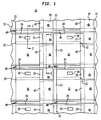
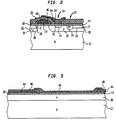
- FIGS. of the drawings are not necessarily drawn to scale.
- FIGS, 1, 2 and 3 there is shown a solid-state image sensor 10 in accordance with the present invention.
- FIG. 1 is a top view. To simplify FIG. 1, metal contacts are not shown and it assumed that dielectric layers thereof are transparent.
- FIG. 2 is a sectional view taken along line 2-2 of FIG. 1.
- FIG. 3 is a sectional view taken along line 3-3 of FIG. 1.
- Image sensor 10 comprises a substrate 12 of a semiconductor material, such as single crystalline silicon, of one conductivity type, such as p-type, having a major surface 14.
- the photodetectors 16 are arranged in lines, such as rows and columns, to form an area array.
- a shift register 18 shown as a CCD shift register, which extends along a line of the photodetectors 16.
- a drain 20 with an anti-blooming barrier 22 being between each drain 20 and its adjacent photodetector 16.
- a shutter gate 24 for controlling the potential barrier between the photodetector 16 and the drain 20 of the adjacent photodetector 16.
- a sepate transfer gate 42 is shown between each of the photodiodes 16 and shift registers 18.
- each photodetector 16 is a photodiode formed in a portion of substrate 12 and comprises a first region 26 of a conductivity type opposite that of the substrate 12, shown as n-type, and a second region 28 which is within a portion of region 26 and is of the same conductivity type as the substrate 12, shown as p-type, and which extends to the major surface 14.
- the conductivity of the first region 26 is about 1017 impurities/cm3.
- the conductivity of the second region 28 is about 1017 impurities/cm3.
- the second region 28 forms a pn junction 30 with the first region 26.
- the first region 26 extends under the drain 20 and the anti-blooming barrier 22, and the second region 28 extends to the anti-blooming barrier region 34.
- the second region 28 is connected to ground through channel stop regions 21 (shown only in FIG. 1) which extend along the photodiodes 16.
- the substrate 12, first region 26 and second region 28 form a "pinned" diode. Although other types of photodiodes can be used, a "pinned" diode is preferable since it eliminates differences in reset levels resulting from the separate gates 24 and 42.
- Thel drain 20 comprises a region 32 of the same conductivity type as the first region 26 but of higher conductivity, shown as n+ type, in the substrate 12 and extending to the major surface 14 and within a portion of the first region 26.
- the conductivity of the drain region 32 is about 1019 impurities/cm3.
- the anti-blooming barrier 22 is a virtual gate and comprises a region 34 of the same conductivity type as the second region 28 but of higher conductivity, shown as p+ type, in the substrate 12 and extending to the major surface 14 and within a portion of the first region 26.
- the anti-blooming barrier region 34 is of a conductivity of about 1018 impurities/cm3.
- the anti-blooming barrier region 34 extends along an edge of the second region 28 between the second region 28 and the drain region 32.
- each of the CCD shift registers 18 comprises a buried channel 36 comprising a region of a conductivity type opposite that of the aubstrate 12, shown as n-type, in the substrate 12 and extending to the major surface 14.
- the channel region 36 is typically of a conductivity of about 1017 impurities/cm3.
- the channel region 36 extends between two columns of the photodetectors 16 for the full length of the columns with the channel region 36 being spaced from the photodetectors 16 in both of the adjacent columns.
- a thin layer 38 of an insulating materiel, typically silicon dioxide, is on the major surface 14 over the channel region 36 and the areas of the major surface 14 between adjacent photodetectors 16 in each column.
- a first set of CCD gates 40 are on the silicon dioxide layer 38 and are spaced along the channel region 36. Each of the first gates 40 contacts one of the transfer gates 42 which extends actoss the space between the channel region 36 and the first region 26 of the photodetector 16 and serves as a transfer gate.
- a second set of CCD gates 44 are on the silicon dioxide layer 38 with each second gate 44 being between a pair of the first gates 40. Each of the first gates 40 overlaps a portion of each of its adjacent second sates 44 and is insulated therefrom by a layer of an insulating material 46, typically silicon dioxide.
- a transfer region, not shown, of a conductivity type opposite that of the channel region 36 may be provided in the channel region under an edge of each gate 40 and 44.
- the gates 24, 40, 42, 44 and 48 are of a conductive material, typically doped polycrystalline silicon.
- the shutter gate 24 is an extension of one of the second gates 44 which is on the silicon dioxide layer 38 and extends across the space between the first regions 26 of adjacent photodetectors 16 in each column.
- Each of the gates 42 has an extension 48 which extends over a shutter gate 24 and is insulated therefrom by a portion of the silicon dioxide layer 46.
- a thick layer 50 of an insulating material, typically silicon dioxide, extends over the photodetectors 16 and the CCD shift registers 18 to protect them.
- a conductive contact 52 which may be a film of a metal, extends through an opening 54 in the insulating layer 50 to make contact with each drain region 32 so as to allow each drain 20 to be connected to a voltage source.
- the contact layer 52 also extends over the adjacent shutter gate 24 and CCD shift registers 18 of FIG. 1 to shield these regions from the impinging light.
- the potential 22P in the anti-blooming barrier region 34 is lower than the potentials 16P and 20P in the photodetector 16 and drain 20 respectively because of the higher doping level in the barrier region 34.
- the potential 22P is higher than the potential under the CCD transfer gate 42.
- the photodetectors 16 are reset. As shown in FIG. 5, the photodetectors 16 are reset by applying a voltage to the shutter gates. 24 through the second gates 44 of the CCD shift register so as to raise the potential 24P under the shutter gates 24 to a level above the potential 16P in the photodetectors 16. This allows the charge carriers in the photodetectors 16 to flow across the area under the shutter gates 24 into the drain 20 as indicated by the arrow 56. Once the photodetectors 16 have been dumped of the charge carriers, the voltage on the shutter gate 24 is lowered to provide the potential barrier 24P shown in FIG. 4.
- the charge carriers collected in the photodetectors 16 during the exposure time are transferred to the CCD shift register 18. This is achieved by applying a potential to each of the first gates 40 so that the potential under each transfer gate 42 is raised above that in the photodetectors 16. The charge carriers will then flow across the space under the transfer gates 42 into the shift register channel 36. Although, the first gates 42 have an extension 48 over the area between each photodetector 16 and the drain 20 of the adjacent photodetector 16, the effect of the voltage on the gate extension 48 is shielded by the shutter gate 24. Thus, the voltage on the first gates 42 does not cause the charge carriers in the photodetectors 16 to flow into the drains 20 of the adjacent photodetectors 16.
- the CCD shift register 18 is then operated in the normal manner to transfer the charge carriers along the shift register 18 to a read-out of the imager 10.
- the voltages applied to the gates 40 and 44 to move the charge carriers along the channel region 32 are less than those applied to the gates during the reset and transfer periods so as not to reduce the barriers under transfer gate 42 and exposure gate 24.
- a solid state image sensor 10 in which the drain 20 serves the dual purpose of an anti-blooming drain and a drain for resetting the photodetectors 16 to achieve a desired exposure control.
- the exposure control shutter 24 is a part of the gates of the CCD shift registers 18 and merely extends across the necessary space between adjacent photodetectors 16 in each column.
- both exposure control and anti-blooming are achieved using a minimum number of elements and without taking up any substantial amount of additional space on the substrate 12 so that the fill factor of the imager is not substantially lowered.
- the solid-state image sensor 10 has been shown as having pn junction type photodiodes as the photodetectors 16, other types of photodetectors can be used.
- the shift registers 18 have been shown as being CCD shift registers, another type of shift register can be used which has a gate which can also be used as the shutter gate 24.
Landscapes
- Solid State Image Pick-Up Elements (AREA)
- Transforming Light Signals Into Electric Signals (AREA)
Claims (10)
- Halbleiter-Bildsensor bestehend aus:- einem Substrat aus dem Halbleitermaterial (12) eines Leitfähigkeitstyps mit einer Hauptfläche (14);- einer Vielzahl von im Substrat (12) an der Hauptfläche in Reihen und Spalten (14) angeordneten Fotodetektoren (16);- Schieberegistern (18), die sich benachbart zu und entlang jeder Spalte von Fotodetektoren erstrecken;- Mitteln (42) zum selektiven übertragen von Ladungsträgern von jedem Fotodetektor (16) zum benachbarten Schieberegister (18);- einer jedem Fotodetektor (16) zugeordneten Drain-Elektrode (20), die in dem die Fotodetektoren spaltenweise voneinander trennenden Zwischenraum angeordnet ist;- einer zwischen jedem Fotodetektor (16) und der ihm zugeordneten Drain-Elektrode (20) angeordneten Potentialsperrschicht (22), die den übergang von Ladungsträgern vom Fotodetektor (16) zur Drain-Elektrode derart steuert, daß ein überstrahlen verhindert wird; und- einem Verschlußgatter(24), das sich von einem Gatter des benachbarten Schieberegisters (18) über den Zwischenraum zwischen spaltenweise benachbarten Fotodetektoren erstreckt, um die Ladungsträger jedes Fotodetektors selektiv zur Drain-Elektrode (20) des anderen in der Spalte benachbarten Fotodetektors zur Rückstellung jedes Fotodetektors zu übertragen.
- Bildsensor nach Anspruch 1, dadurch gekennzeichnet, daß im Substrat an der Hauptfläche (14) jeder Fotodetektor (16) einen ersten Bereich (26) von entgegengesetztem Leitfähigkeitstyp und die Drain-Elektrode einen Bereich (32) von entgegengesetztem Leitfähigkeitstyp innerhalb des ersten Bereichs des ihr zugeordneten Fotodetektors und benachbart zu einer Kante des ersten Bereichs aufweisen.
- Bildsensor nach Anspruch 1 oder 2, dadurch gekennzeichnet, daß die Potentialspekrschicht (22) im Substrat an der Hauptfläche sowie innerhalb des ersten Bereichs (26) und sich quer über diesen erstreckend einen hochleitfähigen Sperrbereich (34) des einen Leitfähigkeitstyps aufweist.
- Bildsensor nach Anspruch 2 oder 3, dadurch gekennzeichnet, daß das Verschlußgatter (24) oberhalb der Hauptfläche (14) und gegenüber dieser isoliert ein sich über den Zwischenraum zwischen benachbarten ersten Bereichen (26) spaltenweise benachbarter Fotodetektoren erstrekkendes leitendes Gatter aufweist.
- Bildsensor nach Anspruch 4, dadurch gekennzeichnet, daß jeder Fotodetektor im Substrat an der Hauptfläche (14) und innerhalb des ersten Bereichs (26) einen zweiten Bereich (28) des einen Leitfähigkeitstyps aufweist.
- Bildsensor nach Anspruch 5, dadurch gekennzeichnet, daß der Sperrbereich (34) eine höhere Leitfähigkeit als der zweite Bereich des Fotodetektors aufweist und sich entlang einer Kante des zweiten Bereichs zwischen dem zweiten Bereich (28) und dem benachbarten Bereich (32) der Drain-Elektrode erstreckt.
- Bildsensor nach Anspruch 6, dadurch gekennzeichnet, daß jedes Schieberegister (18) ein ladungsgekoppeltes Schieberegister ist, das einen Kanalbereich (36), der sich in den benachbarten Spalten entlang der Fotodetektoren (16) und von diesen beabstandet erstreckt, und eine Vielzahl von leitenden Gattern (40,44) aufweist, die sich über die Hauptfläche und gegenüber dieser isoliert sowie quer über den Kanalbereich (36) erstrecken.
- Bildsensor nach Anspruch 7, dadurch gekennzeichnet, daß das Schieberegister (18) eine erste Gruppe leitender, im Abstand entlang des Kanalbereichs (36) angeordneter Gatter (40) und eine zweite Gruppe leitender, in den Lücken zwischen den Gattern der ersten Gruppe angeordneter Gatter aufweist.
- Bildsensor nach Anspruch 8, dadurch gekennzeichnet, daß die Mittel zum selektiven übertragen von Ladungsträgern von den Fotodetektoren zum Schieberegister eine Verlängerung (42) jedes Gatters (40) der ersten Gruppe aufweisen, die sich quer über den Zwischenraum zwischen einem Fotodetektor (16) und dem Kanalbereich (36) erstreckt.
- Bildsensor nach Anspruch 9, dadurch gekennzeichnet, daß jedes der Verschlußgatter (24), das sich zwischen spaltenweise benachbarten Fotodetektoren (16) erstreckt, eine Verlängerung eines der Gatter (44) der zweiten Gruppe von Gattern des benachbarten Schieberegisters (18) bildet.
Applications Claiming Priority (3)
| Application Number | Priority Date | Filing Date | Title |
|---|---|---|---|
| US420869 | 1989-10-12 | ||
| US07/420,869 US4974043A (en) | 1989-10-12 | 1989-10-12 | Solid-state image sensor |
| PCT/US1990/005496 WO1991006124A1 (en) | 1989-10-12 | 1990-10-01 | Solid-state image sensor |
Publications (2)
| Publication Number | Publication Date |
|---|---|
| EP0453530A1 EP0453530A1 (de) | 1991-10-30 |
| EP0453530B1 true EP0453530B1 (de) | 1996-01-31 |
Family
ID=23668168
Family Applications (1)
| Application Number | Title | Priority Date | Filing Date |
|---|---|---|---|
| EP90915584A Expired - Lifetime EP0453530B1 (de) | 1989-10-12 | 1990-10-01 | Festkörper-bildsensor |
Country Status (5)
| Country | Link |
|---|---|
| US (1) | US4974043A (de) |
| EP (1) | EP0453530B1 (de) |
| JP (1) | JPH04502236A (de) |
| DE (1) | DE69025173T2 (de) |
| WO (1) | WO1991006124A1 (de) |
Families Citing this family (11)
| Publication number | Priority date | Publication date | Assignee | Title |
|---|---|---|---|---|
| US5130774A (en) * | 1990-07-12 | 1992-07-14 | Eastman Kodak Company | Antiblooming structure for solid-state image sensor |
| US6356305B1 (en) * | 1997-01-30 | 2002-03-12 | Nikon Corporation | Image-pickup apparatus and method for reading accumulated signal changes through transfer lines |
| US5929471A (en) * | 1997-05-30 | 1999-07-27 | Dalsa, Inc. | Structure and method for CCD sensor stage selection |
| US6100552A (en) * | 1998-01-14 | 2000-08-08 | Dalsa, Inc. | Multi-tapped bi-directional CCD readout register |
| US5990503A (en) * | 1998-01-14 | 1999-11-23 | Dalsa, Inc. | Selectable resolution CCD sensor |
| JPH11274454A (ja) * | 1998-03-19 | 1999-10-08 | Canon Inc | 固体撮像装置及びその形成方法 |
| TW425563B (en) * | 1998-06-03 | 2001-03-11 | Nippon Electric Co | Solid state image pickup device and driving method therefore |
| US6331873B1 (en) * | 1998-12-03 | 2001-12-18 | Massachusetts Institute Of Technology | High-precision blooming control structure formation for an image sensor |
| KR101016539B1 (ko) * | 2002-08-12 | 2011-02-24 | 소니 주식회사 | 고체 촬상 소자 및 그 제조 방법 |
| JP4613305B2 (ja) * | 2004-10-19 | 2011-01-19 | 国立大学法人静岡大学 | 埋め込みフォトダイオード構造による撮像装置 |
| US9369648B2 (en) * | 2013-06-18 | 2016-06-14 | Alexander Krymski | Image sensors, methods, and pixels with tri-level biased transfer gates |
Family Cites Families (10)
| Publication number | Priority date | Publication date | Assignee | Title |
|---|---|---|---|---|
| JPS5795771A (en) * | 1980-12-05 | 1982-06-14 | Fuji Photo Film Co Ltd | Solid-state image pickup device |
| JPS5819080A (ja) * | 1981-07-27 | 1983-02-03 | Sony Corp | 固体撮像素子 |
| US4696021A (en) * | 1982-06-03 | 1987-09-22 | Nippon Kogaku K.K. | Solid-state area imaging device having interline transfer CCD means |
| JPS60254770A (ja) * | 1984-05-31 | 1985-12-16 | Fujitsu Ltd | イメージセンサ |
| US4679212A (en) * | 1984-07-31 | 1987-07-07 | Texas Instruments Incorporated | Method and apparatus for using surface trap recombination in solid state imaging devices |
| US4613402A (en) * | 1985-07-01 | 1986-09-23 | Eastman Kodak Company | Method of making edge-aligned implants and electrodes therefor |
| GB8517081D0 (en) * | 1985-07-05 | 1985-08-14 | Gen Electric Co Plc | Image sensors |
| US4851915A (en) * | 1986-08-11 | 1989-07-25 | Xian Northwest Telecommunication Engineering Inst. | Method and apparatus for obtaining clear images of high speed moving objects |
| US4984047A (en) * | 1988-03-21 | 1991-01-08 | Eastman Kodak Company | Solid-state image sensor |
| FR2631188A1 (fr) * | 1988-05-03 | 1989-11-10 | Thomson Csf | Photodetecteur matriciel a transfert de charges avec dispositif integre de filtrage de charges |
-
1989
- 1989-10-12 US US07/420,869 patent/US4974043A/en not_active Expired - Lifetime
-
1990
- 1990-10-01 DE DE69025173T patent/DE69025173T2/de not_active Expired - Fee Related
- 1990-10-01 JP JP2514521A patent/JPH04502236A/ja active Pending
- 1990-10-01 EP EP90915584A patent/EP0453530B1/de not_active Expired - Lifetime
- 1990-10-01 WO PCT/US1990/005496 patent/WO1991006124A1/en not_active Ceased
Also Published As
| Publication number | Publication date |
|---|---|
| JPH04502236A (ja) | 1992-04-16 |
| US4974043A (en) | 1990-11-27 |
| DE69025173T2 (de) | 1996-08-29 |
| EP0453530A1 (de) | 1991-10-30 |
| WO1991006124A1 (en) | 1991-05-02 |
| DE69025173D1 (de) | 1996-03-14 |
Similar Documents
| Publication | Publication Date | Title |
|---|---|---|
| KR970007711B1 (ko) | 오버-플로우 드레인(ofd)구조를 가지는 전하결합소자형 고체촬상장치 | |
| KR100262774B1 (ko) | 상부 버스 가상 위상 프레임 행간 전송 ccd 영상 감지기 | |
| JP3177514B2 (ja) | 固体イメージセンサ | |
| JP3200436B2 (ja) | Ccd撮像器及びその駆動方法 | |
| US4168444A (en) | Imaging devices | |
| JPS5819080A (ja) | 固体撮像素子 | |
| US5130774A (en) | Antiblooming structure for solid-state image sensor | |
| US5306931A (en) | CCD image sensor with improved antiblooming characteristics | |
| JPS5917581B2 (ja) | 固体撮像装置 | |
| JPS58138187A (ja) | 固体イメ−ジセンサ | |
| US5798542A (en) | Image sensor having ITO electrodes with overlapping color filters for increased sensitivity | |
| KR100265269B1 (ko) | 수직 오버플로우 드레인 및 저항성 게이트 전하 전송소자를 가지는 고체촬상소자 및 그 제어방법 | |
| EP0453530B1 (de) | Festkörper-bildsensor | |
| WO1990016083A1 (en) | Charge-coupled imager with dual gate anti-blooming structure | |
| JP2858179B2 (ja) | Ccd映像素子 | |
| KR101159032B1 (ko) | 고체 촬상 소자 | |
| US5804845A (en) | Image sensor having ITO electrodes with an ONO layer | |
| US5047862A (en) | Solid-state imager | |
| JP2917361B2 (ja) | 固体撮像素子 | |
| JPH0642540B2 (ja) | ブルーミング防止障壁を有する電荷転送デバイス | |
| US4654683A (en) | Blooming control in CCD image sensors | |
| EP0756759B1 (de) | Ladungsgekoppelte bildaufnahmeanordnung | |
| JPS6134263B2 (de) | ||
| KR950002194B1 (ko) | 프레임 트랜스퍼방식의 ccd 영상센서 | |
| JPH0697416A (ja) | 固体撮像装置及びその製造方法 |
Legal Events
| Date | Code | Title | Description |
|---|---|---|---|
| PUAI | Public reference made under article 153(3) epc to a published international application that has entered the european phase |
Free format text: ORIGINAL CODE: 0009012 |
|
| AK | Designated contracting states |
Kind code of ref document: A1 Designated state(s): DE FR GB |
|
| 17P | Request for examination filed |
Effective date: 19911019 |
|
| 17Q | First examination report despatched |
Effective date: 19931125 |
|
| GRAA | (expected) grant |
Free format text: ORIGINAL CODE: 0009210 |
|
| AK | Designated contracting states |
Kind code of ref document: B1 Designated state(s): DE FR GB |
|
| REF | Corresponds to: |
Ref document number: 69025173 Country of ref document: DE Date of ref document: 19960314 |
|
| ET | Fr: translation filed | ||
| PG25 | Lapsed in a contracting state [announced via postgrant information from national office to epo] |
Ref country code: GB Effective date: 19961001 |
|
| PLBE | No opposition filed within time limit |
Free format text: ORIGINAL CODE: 0009261 |
|
| STAA | Information on the status of an ep patent application or granted ep patent |
Free format text: STATUS: NO OPPOSITION FILED WITHIN TIME LIMIT |
|
| 26N | No opposition filed | ||
| GBPC | Gb: european patent ceased through non-payment of renewal fee |
Effective date: 19961001 |
|
| PG25 | Lapsed in a contracting state [announced via postgrant information from national office to epo] |
Ref country code: FR Effective date: 19970630 |
|
| PG25 | Lapsed in a contracting state [announced via postgrant information from national office to epo] |
Ref country code: DE Effective date: 19970701 |
|
| REG | Reference to a national code |
Ref country code: FR Ref legal event code: ST |