EP0452981B1 - Régulateur résonant limité en fréquence - Google Patents
Régulateur résonant limité en fréquence Download PDFInfo
- Publication number
- EP0452981B1 EP0452981B1 EP91110240A EP91110240A EP0452981B1 EP 0452981 B1 EP0452981 B1 EP 0452981B1 EP 91110240 A EP91110240 A EP 91110240A EP 91110240 A EP91110240 A EP 91110240A EP 0452981 B1 EP0452981 B1 EP 0452981B1
- Authority
- EP
- European Patent Office
- Prior art keywords
- voltage
- frequency
- coupled
- amplifier
- operating frequency
- Prior art date
- Legal status (The legal status is an assumption and is not a legal conclusion. Google has not performed a legal analysis and makes no representation as to the accuracy of the status listed.)
- Expired - Lifetime
Links
Images
Classifications
-
- G—PHYSICS
- G05—CONTROLLING; REGULATING
- G05F—SYSTEMS FOR REGULATING ELECTRIC OR MAGNETIC VARIABLES
- G05F1/00—Automatic systems in which deviations of an electric quantity from one or more predetermined values are detected at the output of the system and fed back to a device within the system to restore the detected quantity to its predetermined value or values, i.e. retroactive systems
- G05F1/10—Regulating voltage or current
- G05F1/12—Regulating voltage or current wherein the variable actually regulated by the final control device is ac
- G05F1/13—Regulating voltage or current wherein the variable actually regulated by the final control device is ac using ferroresonant transformers as final control devices
-
- H—ELECTRICITY
- H02—GENERATION; CONVERSION OR DISTRIBUTION OF ELECTRIC POWER
- H02M—APPARATUS FOR CONVERSION BETWEEN AC AND AC, BETWEEN AC AND DC, OR BETWEEN DC AND DC, AND FOR USE WITH MAINS OR SIMILAR POWER SUPPLY SYSTEMS; CONVERSION OF DC OR AC INPUT POWER INTO SURGE OUTPUT POWER; CONTROL OR REGULATION THEREOF
- H02M3/00—Conversion of dc power input into dc power output
- H02M3/22—Conversion of dc power input into dc power output with intermediate conversion into ac
- H02M3/24—Conversion of dc power input into dc power output with intermediate conversion into ac by static converters
- H02M3/28—Conversion of dc power input into dc power output with intermediate conversion into ac by static converters using discharge tubes with control electrode or semiconductor devices with control electrode to produce the intermediate ac
- H02M3/325—Conversion of dc power input into dc power output with intermediate conversion into ac by static converters using discharge tubes with control electrode or semiconductor devices with control electrode to produce the intermediate ac using devices of a triode or a transistor type requiring continuous application of a control signal
- H02M3/335—Conversion of dc power input into dc power output with intermediate conversion into ac by static converters using discharge tubes with control electrode or semiconductor devices with control electrode to produce the intermediate ac using devices of a triode or a transistor type requiring continuous application of a control signal using semiconductor devices only
- H02M3/337—Conversion of dc power input into dc power output with intermediate conversion into ac by static converters using discharge tubes with control electrode or semiconductor devices with control electrode to produce the intermediate ac using devices of a triode or a transistor type requiring continuous application of a control signal using semiconductor devices only in push-pull configuration
- H02M3/3376—Conversion of dc power input into dc power output with intermediate conversion into ac by static converters using discharge tubes with control electrode or semiconductor devices with control electrode to produce the intermediate ac using devices of a triode or a transistor type requiring continuous application of a control signal using semiconductor devices only in push-pull configuration with automatic control of output voltage or current
-
- Y—GENERAL TAGGING OF NEW TECHNOLOGICAL DEVELOPMENTS; GENERAL TAGGING OF CROSS-SECTIONAL TECHNOLOGIES SPANNING OVER SEVERAL SECTIONS OF THE IPC; TECHNICAL SUBJECTS COVERED BY FORMER USPC CROSS-REFERENCE ART COLLECTIONS [XRACs] AND DIGESTS
- Y02—TECHNOLOGIES OR APPLICATIONS FOR MITIGATION OR ADAPTATION AGAINST CLIMATE CHANGE
- Y02B—CLIMATE CHANGE MITIGATION TECHNOLOGIES RELATED TO BUILDINGS, e.g. HOUSING, HOUSE APPLIANCES OR RELATED END-USER APPLICATIONS
- Y02B70/00—Technologies for an efficient end-user side electric power management and consumption
- Y02B70/10—Technologies improving the efficiency by using switched-mode power supplies [SMPS], i.e. efficient power electronics conversion e.g. power factor correction or reduction of losses in power supplies or efficient standby modes
Definitions
- This invention relates to resonant regulator power supplies.
- EP-A-107003 and EP-A-107770 each discloses a resonant power supply having a source of alternating voltage of controllable frequency, a resonant circuit excited by the source, means coupled to the resonant circuit for generating an output voltage and a control circuit responsive to the output voltage to control the frequency of operation of the source to regulate the output voltage.
- the control circuit includes a limiting circuit for preventing the frequency of operation of the source passing through the resonance frequency of the resonant circuit.
- the resonant circuit is a parallel resonant circuit.
- the resonant circuit is a series resonant circuit.
- FR-A-8007449 (US-A-4336584) relates to a resonant regulator which varies the frequency of operation to regulate the output voltage. There is no provision to avoid resonance.
- a resonant regulator operating on the positive slope of the resonant transfer characteristic curve regulates in an operating frequency range below the resonance frequency of the resonant circuit. If the control circuit of the resonant regulator attempts to locate the operating point above resonance, regulation is lost since the feedback changes from negative to positive feedback.
- the frequency control loop is therefore designed to avoid placing the operating point of the regulator on the side of the resonance frequency curve producing positive feedback under all expected operating conditions.
- the elements of the frequency control loop are subject to tolerances in the values of the resonant L and C components, to tolerances in the voltage feedback components, such as voltage divider resistors, and generally to tolerances throughout the control loop. Because of the large number of elements associated with the frequency control loop, it is relatively impractical to hold all tolerances small enough to insure that the operating point of the resonant regulator is below the resonance frequency under all foreseeable operating conditions. This is especially true when it is desirable to operate very close to the resonance frequency, where the slope of resonant transfer characteristic curve is steep and provides good loop response.
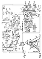
- a source 21 of AC mains voltage is coupled between input terminals 22 and 23 of a full-wave bridge rectifier 19, to develop a DC unregulated input voltage V in between a supply terminal 24 and a current return or ground terminal 25 that is electrically nonisolated from mains source 21.
- Filtering of voltage V in is provided by equal-valued, series-coupled, capacitors C1 and C2.
- the unregulated DC voltages V il and V i2 developed across respective capacitors C1 and C2, are substantially equal in magnitude, at one-half the magnitude of voltage V in .
- a voltage regulator 33 supplies a low DC voltage +V for the control circuitry of resonant regulator 20.
- An LC resonant circuit 10 includes an inductor L0 and a capacitor C0 series coupled at one end to an intermediate supply terminal 26 via a DC blocking capacitor C3, and at the other end to a square-wave input terminal 30.
- Resonant circuit 10 is coupled to and excited by a source 40 of alternating, square-wave, input voltage V sq , controllable in frequency f.
- Square-wave voltage source 40 comprises a frequency controllable oscillator 41, that generates a square-wave oscillator voltage V osc , a driver stage 42, and push-pull switches S1 and S2.
- switch S1 is coupled between supply terminal 24 and square-wave input terminal 30, and switch S2 is coupled between input terminal 30 and nonisolated ground.
- the output of driver 42 is inverted by an inverter 43 before being applied to switch S2.
- Capacitor C3 blocks any residual DC introduced by asymmetrical switching operation or by unequal values for capacitors C1 and C2.
- square-wave input voltage V sq excites resonant circuit 10 into oscillation to develop a generally sinusoidal supply voltage V0 across resonant capacitor C0.
- Voltage V0 has a fundamental frequency at the exciting or operating frequency f of square-wave input voltage V sq .
- the voltage developed across resonant inductor L0 is also a generally sinusoidal wave of frequency f that, however, exhibits step changes in voltage magnitude during leading and trailing edge transitions of voltage V sq .
- the phasing between square-wave voltage V sq and the sinusoidal components of the inductive and capacitive voltage varies with load and with AC mains voltage variations.
- a primary winding W1 of a power transformer T1 is coupled across resonant capacitor C0 of resonant circuit 10.
- the inductance exhibited by winding W1 may affect the resonance frequency of resonant circuit 10, depending on its value relative to that of inductor L0.
- Voltage V0 is applied across primary winding W1 and develops sinusoidal output voltages across tightly coupled secondary windings W3-W5. These voltages are rectified and filtered by respective elements 27-29 to develop respective DC supply voltages V1-V3 that energize respective load circuits not shown in FIGURE 1.
- Power transformer T1 also provides electrical shock hazard isolation between mains voltage source 21 and the load circuits energized by supply voltages V1-V3. Thus, the current return path or ground termination for the secondary side load circuits of transformer T1 is electrically isolated from ground 25 on the primary side.
- a frequency control circuit 50 forms a negative feedback loop that regulates supply voltages V1-V3 with variations in main supply voltage and loading.
- one of the output voltages illustratively voltage V1 is directly coupled to the emitter of a PNP error amplifier transistor Q1 via a level shifting, voltage reference, zener diode Z1.
- Voltage V1 is also coupled to the base of transistor Q1 via a voltage divider resistance network R1-R4, with the base being coupled to an adjustable intermediate point of the voltage divider.
- the collector of transistor Q1 is coupled via a collector load resistor R8 to an input pin 1 of an opto-isolator amplifier U3 for developing a feedback voltage V f across load resistor R16 coupled to an output pin 4.
- Amplifier U3 may be selected as opto-isolator CNY51, manufactured by the Semiconductor Products Department, General Electric Company, Auburn, New York.
- Feedback voltage V f is coupled to a noninverting input terminal of an amplifier U1 to develop at the output of amplifier U1 a frequency control voltage V c1 .
- the inverting input terminal of amplifier U1 is grounded via a resistor R17.
- Linear operation of amplifier U1 is provided by feeding back voltage V c1 to the inverting input terminal via resistors R18 and R19.
- the gain of amplifier U1 is determined by the value of this feedback resistance.
- frequency control voltage V c1 is applied to a frequency control input pin 4 of oscillator 41 via a resistor R20 and a pass-through diode D4.
- the frequency control voltage V co that is developed across a resistor R21 coupled to frequency control pin 4, varies in accordance with feedback frequency control voltage V c1 .
- FIGURE 2 illustrates typical resonant transfer characteristic curves associated with the operation of resonant regulator 20.
- Frequency control circuit 50 controls operating frequency f so as to establish an operating point P1 on curve 31 at a frequency f1 that regulates output supply voltage V1 to its desired level. From the location of operating point P1 on the positive slope of transfer characteristic curve 31, one notes that frequency control circuit 50 is designed to regulate at frequencies below, or to the left side of, resonance frequency f res .
- the resonant transfer characteristic curve of resonant circuit 10 for the new operating condition is curve 32 of FIGURE 2.
- the resonance frequency for curve 32 will be very close to that of resonance frequency f res of curve 31. Due, however, to the increased loading on resonant circuit 10, the peak of curve 32 is lower than that of curve 31, and the slope of the curve on either side of resonance is less steep.
- Frequency control circuit 50 operates in the following manner to, for example, increase the operating frequency as increased loading attempts to decrease supply voltage V1.
- the decrease in supply voltage V1 being directly coupled to the emitter of transistor Q1 via zener diode Z1, while being only proportionally coupled to the base via divider R1-R4, produces a decrease in transistor conduction.
- the decrease in conduction of transistor Q1 produces a decrease in feedback voltage V f that is amplified by amplifier U1 to produce a decrease in frequency control voltage V c1 .
- the decrease in frequency control voltage V c1 is passed through diode D4 as a decrease in oscillator frequency control voltage V co developed at frequency control pin 4 of the oscillator.
- resonant regulator 20 It may be desirable to design resonant regulator 20 to have a normal operating frequency range that closely approaches the resonance frequency of resonant circuit 10 at the extremes of the operating range. Such a design choice insures that the regulator operates on the relatively steep portion of the resonant transfer characteristic curve, thereby providing good loop response and a relatively wide range of regulation.
- the operating point of the regulator on a given transfer characteristic curve may be so close to the resonance frequency that frequency control circuit 50 will attempt to locate the operating point on the negative slope of, for example, curve 32. Should a situation arise where the operating frequency passes through the resonance frequency regulation is completely lost, because frequency control circuit 50 will now operate in a positive feedback mode. For example, control circuit 50 will respond to a decrease in supply voltage V1 by increasing rather than decreasing the operating frequency, which produces a further decrease in supply voltage.
- resonant regulator 20 includes a frequency limiting circuit 60 that prevents the operating frequency from passing through resonance.
- a frequency limiting circuit 60 that prevents the operating frequency from passing through resonance.
- the operating frequency is near but below resonance, the AC voltage across capacitor C O is greater than the AC voltage across inductor L O .
- the operating frequency slightly exceeds resonance, the AC voltage across inductor L O is greater than the AC voltage across capacitor C O .
- the AC voltages across capacitor C O and inductor L O are equal.
- the voltage developed by inductive element L0 of resonant circuit 10 is sensed by a secondary winding W s magnetically coupled to inductor L0.
- Frequency limiting circuit 60 also senses the amplitude of voltage V0 developed across capacitive element C0 of resonant circuit 10.
- the capacitive voltage is sensed by a secondary winding W2 of transformer T1 that is tightly coupled with primary winding W1.
- the voltage V CAC across winding W2 is a transformed voltage representative of capacitive voltage V0. Without regulation, the AC voltage across capacitor C0 decreases with increasing operating frequency. However, the amplitude of voltage V CAC tends to remain unchanged under normal operating conditions due to the regulation provided by resonant regulator 20.
- Capacitive voltage V CAC is lowpass filtered by a resistor R5 and a capacitor C5, rectified by a diode D1 to charge a capacitor C8 that develops a positive DC sense voltage +V C , having a magnitude that is in accordance with the amplitude of voltage V CAC .
- Inductive voltage V LAC is lowpass filtered by a resistor R6 and a capacitor C6, rectified by a diode D2 to charge a capacitor C9 that develops a negative DC sense voltage -V L having a magnitude that is in accordance with the amplitude of voltage V LAC .
- Capacitive sense voltage +V C and inductive sense voltage -V L are algebraically summed via respective resistors R9 and R10 to develop a difference voltage V dif across a resistor R11 coupled to a summing junction terminal 34.
- Voltage V dif is therefore related to the difference in magnitudes between the capacitive sense voltage and the inductive sense voltage, or V dif ⁇ (V C -V L ).
- Voltage V dif is applied to the inverting input terminal of an amplifier U2 having a noninverting input terminal that is grounded.
- the output of amplifier U2 is coupled to frequency control pin 4 of oscillator 41 via a resistor R15 and a diode D3.
- Negative feedback for amplifier U2 is provided by resistors R13 and R14 series coupled between the output terminal and the inverting input terminal.
- Amplifiers U1 and U2 may each be selected as CA3140, manufactured by the Solid State Division of RCA Corporation, Somerville, New Jersey.
- resonant circuit 10 When the AC voltages across inductor L O and capacitor C O are equal, resonant circuit 10 is operating at its resonant frequency.
- the embodiment provides an arrangement for limiting the operating frequency to a predetermined amount below resonance by limiting the increase in operating frequency in response to a predetermined minimum difference between the voltages across inductor L O and capacitor C O . Since such voltage difference does not decrease beyond its predetermined minimum value, the resonant frequency of resonant circuit 10 is never reached.
- the magnitude of inductive sense voltage V L is maintained smaller than the magnitude of the capacitance sense voltage V C , within the normal operating frequency range below resonance.
- the difference voltage V dif is a positive value.
- a positive voltage V dif when applied to the inverting input terminal of amplifier U2, produces cutoff of amplifier U2. Since the voltage at frequency control pin 4 is positive during normal operation of resonant regulator 20, diode D3 is reverse biased and blocks the voltage at the output of amplifier U2 from passing through to pin 4 and affecting the normal operation of the negative feedback loop formed by frequency control circuit 50.
- the feedback resistance of amplifier U2 is selected to be much greater than the feedback resistance of amplifier U1, illustratively 10 or more times greater.
- the voltage gain of amplifier U2 is therefore much greater than the voltage gain of amplifier U1.
- Frequency limiting circuit 60 automatically holds the upper frequency limit of operation to a given design guard band below the resonance frequency, even though the resonance frequency itself may vary due to component tolerances, temperature, and aging effects.
- the relative magnitudes of the AC voltages across inductive element L0 and capacitive element C0 of resonant circuit 10 tend to inversely track each other near resonance.
- Voltage V dif which is indicative of the closeness of the operating frequency to resonance, is related to the difference in magnitudes of the inductive and capacitive voltages.
- Voltage V dif is a monotonic function in the region of interest to either side of resonance on the transfer characteristic curve, with voltage V dif reversing polarity as the frequency closes to near resonance.
- voltage limiting circuit 60 may be activated at an amount below resonance that is relatively independent of tolerances, temperature and component aging which would change the resonant frequency itself.
- frequency limit circuit 60 still provides a limiting action.
- the regulator operating point and frequency will be driven to just below resonance to, for example, point P′ m2 , at a high-limit frequency f′ m2 .
- voltage V dif is monotonic through resonance, voltage V dif is able to limit the operating frequency without experiencing a reversal from negative feedback operation to positive feedback operation.
- Frequency limiting circuit 60 advantageously provides frequency limiting under short-circuit load conditions. Should a short-circuit load be developed by power transformer T1, input voltage V0 and capacitive sense voltage +V C will be absent or much reduced in amplitude, while inductive sense voltage -V L will be substantially increased in amplitude. The difference voltage V dif will become negative and drive control voltage V co to a relatively large value that blocks diode D4 and drives the operating frequency below resonance.
- inductor L0 has an inductance of 440 microhenry and a ratio of turns for W s to turns for L0 of 7:67.
- Transformer T1 develops an effective inductance across capacitor C0 of 800 microhenry and a ratio of turns W2 to turns W1 of 5:49.
- Illustrative operating frequencies for nominal component values are the following: an operating frequency of 56.4 kilohertz at a high AC mains voltage of 270 VAC, RMS and at an equivalent load of 100 watts; an operating frequency of 67 kilohertz at a low AC mains voltage of 180 VAC, RMS and at an equivalent load of 100 watts.
- the resonance frequency is approximately 77 kilohertz, with the high-limit frequency being approximately 75.5 kilohertz.
Claims (5)
- Alimentation électrique pour régulateur résonant, comprenant :
une source (S1, S2) de tension d'entrée alternative, qui peut être commandée en fréquence de fonctionnement,
un circuit résonant (10) couplé à et excité par ladite source et comportant associée à lui une fréquence de résonance, ledit circuit résonant comprenant un élément inducteur (L₀) et un élément capacitif (C₀) ;
un moyen (W3) couplé audit circuit résonant (10) pour générer une tension d'alimentation de sortie (V1) ; et
un circuit de commande (50) couplé à ladite source (S1, S2) et sensible à ladite tension d'alimentation de sortie (V1) pour modifier ladite fréquence de fonctionnment suivant une boucle de contre-réaction afin de réguler ladite tension d'alimentation de sortie comprenant un premier amplificateur (U1) pour amplifier une tension de contre-réaction représentative de ladite tension d'alimentation de sortie ; et
un circuit limitateur de fréquence (60) pour empêcher ladite fréquence de fonctionnement de passer par ladite fréquence de résonance ;
caractérisée en ce que le circuit de limitation est couplé au circuit résonant et comprend une source (Ws, W2, R5, R6, R9, C9, R10) de tension de détection de fréquence (Vdif) qui indique la proximité de ladite fréquence de fonctionnement vis à vis de ladite fréquence de résonance et un second amplificateur (U2) possédant une entrée couplée pour recevoir ladite tension de détection et une sortie couplée audit circuit de commande de fréquence (50). - Alimentation électrique selon la revendication 1, dans lequelle le second amplificateur (U2) possède un gain qui est sensiblement plus grand que celui dudit premier amplificateur.
- Alimentation électrique selon la revendication 1 ou 2, comprenant de plus
un moyen (D3, D4) pour combiner les sorties desdits premier (U1) et second (U2) amplificateurs, dans lequel une valeur de sortie dudit premier amplificateur (U1) tend à varier dans un sens donné lorsque ladite fréquence de fonctionnement varie dans une première direction, tandis qu'une valeur de sortie dudit second amplificateur (U2) tend à varier dans un sens opposé. - Alimentation en énergie selon la revendication 1, 2 ou 3 , comprenant de plus
un agencement de commutation (D3, D4) couplé aux deux amplificateurs (U1, U2) pour empêcher ladite source (S1, S2) de tension d'entrée alternative de répondre à ladite tension de détection de fréquence lorsque ladite fréquence de fonctionnement se situe à l'intérieur d'une première gamme de fréquences se trouvant d'un côté de ladite fréquence de résonance et pour empêcher ladite source de répondre à ladite tension de contre-réaction lorsque ladite fréquence de fonctionnement se situe à l'intérieur d'une limite donnée de ladite fréquence de résonance. - Alimentation électrique selon la revendication 4 dans laquelle ledit agencement de commutation comprend des première (D4) et seconde (D3) diodes couplées en série avec les sorties respectives desdits premier (U1) et second (U2) amplificateurs , ladite tension de détection de fréquence bloquant la conduction de ladite première diode (D4) lorsque ladite fréquence de fonctionnement s'approche de ladite fréquence de résonance à l'intérieur de ladite limite donnée .
Applications Claiming Priority (3)
| Application Number | Priority Date | Filing Date | Title |
|---|---|---|---|
| US946867 | 1986-12-29 | ||
| US06/946,867 US4729085A (en) | 1986-12-29 | 1986-12-29 | Frequency limited resonant regulator useful in, for example, a half-bridge inverter |
| EP87311352A EP0275698B1 (fr) | 1986-12-29 | 1987-12-23 | Régulateur résonnant limité en fréquence |
Related Parent Applications (1)
| Application Number | Title | Priority Date | Filing Date |
|---|---|---|---|
| EP87311352.6 Division | 1987-12-23 |
Publications (3)
| Publication Number | Publication Date |
|---|---|
| EP0452981A2 EP0452981A2 (fr) | 1991-10-23 |
| EP0452981A3 EP0452981A3 (en) | 1991-12-27 |
| EP0452981B1 true EP0452981B1 (fr) | 1995-08-23 |
Family
ID=25485087
Family Applications (2)
| Application Number | Title | Priority Date | Filing Date |
|---|---|---|---|
| EP87311352A Expired - Lifetime EP0275698B1 (fr) | 1986-12-29 | 1987-12-23 | Régulateur résonnant limité en fréquence |
| EP91110240A Expired - Lifetime EP0452981B1 (fr) | 1986-12-29 | 1987-12-23 | Régulateur résonant limité en fréquence |
Family Applications Before (1)
| Application Number | Title | Priority Date | Filing Date |
|---|---|---|---|
| EP87311352A Expired - Lifetime EP0275698B1 (fr) | 1986-12-29 | 1987-12-23 | Régulateur résonnant limité en fréquence |
Country Status (10)
| Country | Link |
|---|---|
| US (1) | US4729085A (fr) |
| EP (2) | EP0275698B1 (fr) |
| JP (1) | JPH084384B2 (fr) |
| KR (1) | KR960005611B1 (fr) |
| AT (2) | ATE126946T1 (fr) |
| DE (2) | DE3751480T2 (fr) |
| ES (2) | ES2030745T3 (fr) |
| FI (1) | FI96728C (fr) |
| HK (2) | HK39897A (fr) |
| SG (1) | SG27295G (fr) |
Families Citing this family (13)
| Publication number | Priority date | Publication date | Assignee | Title |
|---|---|---|---|---|
| GB8702299D0 (en) * | 1987-02-02 | 1987-03-11 | British Telecomm | Power supply |
| US4833584A (en) * | 1987-10-16 | 1989-05-23 | Wisconsin Alumni Research Foundation | Quasi-resonant current mode static power conversion method and apparatus |
| US4872100A (en) * | 1988-10-12 | 1989-10-03 | Zenith Electronics Corporation | High voltage DC to AC converter |
| CA2019525C (fr) * | 1989-06-23 | 1995-07-11 | Takuya Ishii | Dispositif d'alimentation a decoupage |
| DE59400222D1 (de) * | 1993-02-05 | 1996-05-30 | Siemens Ag | Verfahren zum Begrenzen der Frequenz eines spannungsgesteuerten Oszillators in einer Steuerschaltung eines Resonanzwandler-Schaltnetzteils und Steuerschaltung für ein Resonanzwandler-Schaltnetzteil |
| JP2001218466A (ja) * | 2000-02-03 | 2001-08-10 | Sony Corp | 高電圧安定化回路 |
| DE10128687A1 (de) * | 2001-06-13 | 2002-12-19 | Philips Corp Intellectual Pty | Spannungswandler |
| US6535399B2 (en) * | 2001-08-14 | 2003-03-18 | Bose Corporation | Tracking power supply controlling |
| JP2004301554A (ja) | 2003-03-28 | 2004-10-28 | Canon Inc | 電位測定装置及び画像形成装置 |
| WO2007129468A1 (fr) * | 2006-05-10 | 2007-11-15 | Masatoshi Imori | retour permettant de stabiliser la tension CC produite À partir d'un circuit de rÉsonance |
| JP5412651B2 (ja) * | 2006-05-10 | 2014-02-12 | 正敏 井森 | 共振回路から生成される直流電圧を安定化する帰還回路の構成法 |
| FR2907614B1 (fr) * | 2006-10-19 | 2008-12-26 | Renault Sas | Procede de reglage d'une alimentation electrique a decoupage |
| US8837172B2 (en) * | 2007-09-01 | 2014-09-16 | Masatosi Imori | Carrier wave amplitude control in power source for stabilizing DC voltage by utilizing frequency dependence of resonance |
Family Cites Families (12)
| Publication number | Priority date | Publication date | Assignee | Title |
|---|---|---|---|---|
| US3699424A (en) * | 1971-07-06 | 1972-10-17 | Bell Telephone Labor Inc | Overvoltage protection of dc to dc converters using ferroresonance |
| US3739255A (en) * | 1971-12-16 | 1973-06-12 | D Leppert | High frequency ferroresonant transformer |
| US3894280A (en) * | 1974-04-02 | 1975-07-08 | Western Electric Co | Frequency limited ferroresonant power converter |
| IT1118548B (it) * | 1979-04-04 | 1986-03-03 | Wabco Westinghouse Spa | Convertitore statico autorisonante a regolazione estesa |
| DE2943269A1 (de) * | 1979-10-26 | 1981-05-07 | Brown, Boveri & Cie Ag, 6800 Mannheim | Steuerverfahren und schaltungsanordnung fuer einen schwingkreisumrichter |
| US4301398A (en) * | 1980-05-29 | 1981-11-17 | Exide Electronics Corporation | Method and apparatus for controlling a resonant power module |
| US4460949A (en) * | 1982-09-30 | 1984-07-17 | General Electric Company | High frequency parallel resonant dc-dc converter |
| US4477868A (en) * | 1982-09-30 | 1984-10-16 | General Electric Company | High frequency series resonant dc-dc converter |
| US4504895A (en) * | 1982-11-03 | 1985-03-12 | General Electric Company | Regulated dc-dc converter using a resonating transformer |
| US4631652A (en) * | 1984-11-30 | 1986-12-23 | Rca Corporation | Frequency controlled resonant regulator |
| US4672528A (en) * | 1986-05-27 | 1987-06-09 | General Electric Company | Resonant inverter with improved control |
| US4670832A (en) * | 1986-06-12 | 1987-06-02 | General Electric Company | Resonant inverter having improved control at enablement |
-
1986
- 1986-12-29 US US06/946,867 patent/US4729085A/en not_active Expired - Lifetime
-
1987
- 1987-12-22 FI FI875664A patent/FI96728C/fi not_active IP Right Cessation
- 1987-12-23 DE DE3751480T patent/DE3751480T2/de not_active Expired - Fee Related
- 1987-12-23 ES ES198787311352T patent/ES2030745T3/es not_active Expired - Lifetime
- 1987-12-23 EP EP87311352A patent/EP0275698B1/fr not_active Expired - Lifetime
- 1987-12-23 DE DE8787311352T patent/DE3778524D1/de not_active Expired - Fee Related
- 1987-12-23 ES ES91110240T patent/ES2076415T3/es not_active Expired - Lifetime
- 1987-12-23 EP EP91110240A patent/EP0452981B1/fr not_active Expired - Lifetime
- 1987-12-23 AT AT91110240T patent/ATE126946T1/de not_active IP Right Cessation
- 1987-12-23 AT AT87311352T patent/ATE75332T1/de not_active IP Right Cessation
- 1987-12-28 JP JP62336697A patent/JPH084384B2/ja not_active Expired - Fee Related
- 1987-12-28 KR KR1019870015050A patent/KR960005611B1/ko not_active IP Right Cessation
-
1995
- 1995-02-17 SG SG27295A patent/SG27295G/en unknown
-
1997
- 1997-04-03 HK HK39897A patent/HK39897A/xx not_active IP Right Cessation
- 1997-04-03 HK HK40097A patent/HK40097A/xx not_active IP Right Cessation
Also Published As
| Publication number | Publication date |
|---|---|
| US4729085A (en) | 1988-03-01 |
| KR960005611B1 (ko) | 1996-04-26 |
| HK40097A (en) | 1997-04-11 |
| EP0275698A1 (fr) | 1988-07-27 |
| EP0452981A2 (fr) | 1991-10-23 |
| SG27295G (en) | 1995-08-18 |
| DE3751480T2 (de) | 1996-04-11 |
| DE3751480D1 (de) | 1995-09-28 |
| HK39897A (en) | 1997-04-11 |
| DE3778524D1 (de) | 1992-05-27 |
| FI875664A (fi) | 1988-06-30 |
| ES2076415T3 (es) | 1995-11-01 |
| ATE75332T1 (de) | 1992-05-15 |
| JPH027116A (ja) | 1990-01-11 |
| FI875664A0 (fi) | 1987-12-22 |
| KR880008525A (ko) | 1988-08-31 |
| EP0275698B1 (fr) | 1992-04-22 |
| ATE126946T1 (de) | 1995-09-15 |
| FI96728C (fi) | 1996-08-12 |
| FI96728B (fi) | 1996-04-30 |
| EP0452981A3 (en) | 1991-12-27 |
| JPH084384B2 (ja) | 1996-01-17 |
| ES2030745T3 (es) | 1992-11-16 |
Similar Documents
| Publication | Publication Date | Title |
|---|---|---|
| US4964028A (en) | Current limited quasi-resonant voltage converting power supply | |
| EP0452981B1 (fr) | Régulateur résonant limité en fréquence | |
| US4656412A (en) | Ferroresonant flux coupled battery charger | |
| US4843202A (en) | Magnetron with frequency control for power regulation | |
| US5648716A (en) | Power control circuit for a battery charger | |
| US4366390A (en) | Emergency power unit | |
| US4866590A (en) | Supply having a load invariant auxiliary power supply supplied from a main transformer and a current suppressing inductor | |
| US6088249A (en) | Frequency modulated ballast with loosely coupled transformer | |
| CA1305211C (fr) | Circuit generateur de signal de commande du ballast d'une lampe a decharge | |
| EP0059633B1 (fr) | Alimentation en puissance à commutation | |
| US6141232A (en) | Fixed frequency flyback converter | |
| US4584517A (en) | Self-oscillating DC-DC switching voltage regulator | |
| US4791546A (en) | Voltage regulator circuit | |
| EP0556116B1 (fr) | Circuit de contrÔle de puissance pour cuisinière à chauffage par induction | |
| US5363323A (en) | Power supply with plural outputs supplying dynamic and steady loads | |
| US20030117752A1 (en) | Microprocessor-controlled DC to DC converter with fault protection | |
| US5436820A (en) | Power converter with dual PWM control | |
| US4930063A (en) | Variable resonance regulator for power supply | |
| US4731720A (en) | High-voltage power source apparatus | |
| EP0083216A2 (fr) | Appareil pour stabiliser une source d'alimentation | |
| US20030053322A1 (en) | Power supply regulating | |
| US5861768A (en) | Resolver exciter having a simple power source unit | |
| US20040169977A1 (en) | Overcurrent protection switched mode power supply | |
| JPH06141541A (ja) | 直列共振形コンバータの制御方法及び制御回路 | |
| JPH03253260A (ja) | 過電流垂下点制御方式 |
Legal Events
| Date | Code | Title | Description |
|---|---|---|---|
| PUAI | Public reference made under article 153(3) epc to a published international application that has entered the european phase |
Free format text: ORIGINAL CODE: 0009012 |
|
| 17P | Request for examination filed |
Effective date: 19910705 |
|
| AC | Divisional application: reference to earlier application |
Ref document number: 275698 Country of ref document: EP |
|
| AK | Designated contracting states |
Kind code of ref document: A2 Designated state(s): AT BE DE ES FR GB IT |
|
| PUAL | Search report despatched |
Free format text: ORIGINAL CODE: 0009013 |
|
| AK | Designated contracting states |
Kind code of ref document: A3 Designated state(s): AT BE DE ES FR GB IT |
|
| RAP1 | Party data changed (applicant data changed or rights of an application transferred) |
Owner name: RCA THOMSON LICENSING CORPORATION |
|
| 17Q | First examination report despatched |
Effective date: 19940207 |
|
| GRAA | (expected) grant |
Free format text: ORIGINAL CODE: 0009210 |
|
| AC | Divisional application: reference to earlier application |
Ref document number: 275698 Country of ref document: EP |
|
| AK | Designated contracting states |
Kind code of ref document: B1 Designated state(s): AT BE DE ES FR GB IT |
|
| REF | Corresponds to: |
Ref document number: 126946 Country of ref document: AT Date of ref document: 19950915 Kind code of ref document: T |
|
| ET | Fr: translation filed | ||
| REF | Corresponds to: |
Ref document number: 3751480 Country of ref document: DE Date of ref document: 19950928 |
|
| REG | Reference to a national code |
Ref country code: ES Ref legal event code: FG2A Ref document number: 2076415 Country of ref document: ES Kind code of ref document: T3 |
|
| ITF | It: translation for a ep patent filed |
Owner name: ING. C. GREGORJ S.P.A. |
|
| PLBE | No opposition filed within time limit |
Free format text: ORIGINAL CODE: 0009261 |
|
| STAA | Information on the status of an ep patent application or granted ep patent |
Free format text: STATUS: NO OPPOSITION FILED WITHIN TIME LIMIT |
|
| 26N | No opposition filed | ||
| PGFP | Annual fee paid to national office [announced via postgrant information from national office to epo] |
Ref country code: AT Payment date: 19991209 Year of fee payment: 13 |
|
| PGFP | Annual fee paid to national office [announced via postgrant information from national office to epo] |
Ref country code: BE Payment date: 19991229 Year of fee payment: 13 |
|
| PG25 | Lapsed in a contracting state [announced via postgrant information from national office to epo] |
Ref country code: AT Free format text: LAPSE BECAUSE OF NON-PAYMENT OF DUE FEES Effective date: 20001223 |
|
| PG25 | Lapsed in a contracting state [announced via postgrant information from national office to epo] |
Ref country code: BE Free format text: LAPSE BECAUSE OF NON-PAYMENT OF DUE FEES Effective date: 20001231 |
|
| BERE | Be: lapsed |
Owner name: RCA THOMSON LICENSING CORP. Effective date: 20001231 |
|
| REG | Reference to a national code |
Ref country code: GB Ref legal event code: IF02 |
|
| REG | Reference to a national code |
Ref country code: FR Ref legal event code: D6 |
|
| REG | Reference to a national code |
Ref country code: GB Ref legal event code: 746 Effective date: 20030110 |
|
| PGFP | Annual fee paid to national office [announced via postgrant information from national office to epo] |
Ref country code: ES Payment date: 20041216 Year of fee payment: 18 |
|
| PGFP | Annual fee paid to national office [announced via postgrant information from national office to epo] |
Ref country code: GB Payment date: 20051024 Year of fee payment: 19 |
|
| PGFP | Annual fee paid to national office [announced via postgrant information from national office to epo] |
Ref country code: DE Payment date: 20051216 Year of fee payment: 19 |
|
| PG25 | Lapsed in a contracting state [announced via postgrant information from national office to epo] |
Ref country code: ES Free format text: LAPSE BECAUSE OF NON-PAYMENT OF DUE FEES Effective date: 20051224 |
|
| PGFP | Annual fee paid to national office [announced via postgrant information from national office to epo] |
Ref country code: FR Payment date: 20051226 Year of fee payment: 19 |
|
| PGFP | Annual fee paid to national office [announced via postgrant information from national office to epo] |
Ref country code: IT Payment date: 20061231 Year of fee payment: 20 |
|
| REG | Reference to a national code |
Ref country code: ES Ref legal event code: FD2A Effective date: 20051224 |
|
| PG25 | Lapsed in a contracting state [announced via postgrant information from national office to epo] |
Ref country code: DE Free format text: LAPSE BECAUSE OF NON-PAYMENT OF DUE FEES Effective date: 20070703 |
|
| GBPC | Gb: european patent ceased through non-payment of renewal fee |
Effective date: 20061223 |
|
| REG | Reference to a national code |
Ref country code: FR Ref legal event code: ST Effective date: 20070831 |
|
| PG25 | Lapsed in a contracting state [announced via postgrant information from national office to epo] |
Ref country code: GB Free format text: LAPSE BECAUSE OF NON-PAYMENT OF DUE FEES Effective date: 20061223 |
|
| PG25 | Lapsed in a contracting state [announced via postgrant information from national office to epo] |
Ref country code: FR Free format text: LAPSE BECAUSE OF NON-PAYMENT OF DUE FEES Effective date: 20070102 |