EP0450985A2 - Dünnschichttransistor aus Diamant - Google Patents
Dünnschichttransistor aus Diamant Download PDFInfo
- Publication number
- EP0450985A2 EP0450985A2 EP91303046A EP91303046A EP0450985A2 EP 0450985 A2 EP0450985 A2 EP 0450985A2 EP 91303046 A EP91303046 A EP 91303046A EP 91303046 A EP91303046 A EP 91303046A EP 0450985 A2 EP0450985 A2 EP 0450985A2
- Authority
- EP
- European Patent Office
- Prior art keywords
- layer
- thin film
- diamond
- film transistor
- transistor according
- Prior art date
- Legal status (The legal status is an assumption and is not a legal conclusion. Google has not performed a legal analysis and makes no representation as to the accuracy of the status listed.)
- Granted
Links
Images


Classifications
-
- H—ELECTRICITY
- H10—SEMICONDUCTOR DEVICES; ELECTRIC SOLID-STATE DEVICES NOT OTHERWISE PROVIDED FOR
- H10D—INORGANIC ELECTRIC SEMICONDUCTOR DEVICES
- H10D30/00—Field-effect transistors [FET]
- H10D30/01—Manufacture or treatment
-
- H—ELECTRICITY
- H10—SEMICONDUCTOR DEVICES; ELECTRIC SOLID-STATE DEVICES NOT OTHERWISE PROVIDED FOR
- H10D—INORGANIC ELECTRIC SEMICONDUCTOR DEVICES
- H10D30/00—Field-effect transistors [FET]
- H10D30/60—Insulated-gate field-effect transistors [IGFET]
- H10D30/67—Thin-film transistors [TFT]
- H10D30/674—Thin-film transistors [TFT] characterised by the active materials
- H10D30/6741—Group IV materials, e.g. germanium or silicon carbide
-
- H—ELECTRICITY
- H10—SEMICONDUCTOR DEVICES; ELECTRIC SOLID-STATE DEVICES NOT OTHERWISE PROVIDED FOR
- H10D—INORGANIC ELECTRIC SEMICONDUCTOR DEVICES
- H10D62/00—Semiconductor bodies, or regions thereof, of devices having potential barriers
- H10D62/80—Semiconductor bodies, or regions thereof, of devices having potential barriers characterised by the materials
- H10D62/83—Semiconductor bodies, or regions thereof, of devices having potential barriers characterised by the materials being Group IV materials, e.g. B-doped Si or undoped Ge
- H10D62/8303—Diamond
Definitions
- This invention relates generally to thin film transistors, and more particularly concerns a large area thin film transistor.
- a hydrogenated amorphous silicon is used as the active semiconducting layer. Since the amorphous silicon is photoconductive, incident light must be shielded from the active layer of the thin film transistor to avoid any impact to the on-off ratio of the transistor. A light shielding layer is used to isolate the active layer from incident light. The necessity of a light shielding layer results in additional manufacturing steps, as well as, larger more complex structures for the transistors. Furthermore, since amorphous silicon is used for the active layer, the electric field mobility is low, thereby reducing the current driving power of the transistor. Diamond films naturally exhibit insulating properties and will exhibit semiconductive properties when doped with suitable impurities. For example, Japanese Patent Publication No.
- U-S. Patent No. 4,740,263 issued to lmai et al. in 1988 describes a process for preparing a diamond thin film by electron assisted chemical vapor deposition (EACVD).
- EACVD electron assisted chemical vapor deposition
- a boron doped P-type diamond semiconductor is prepared by the addition of a trace amount of diborane in a mixed gas of hydrogen and a hydrocarbon.
- Also disclosed is a potential use of a P-type diamond film in the field of diodes, especially high-frequency rectification.
- Fujimori "Field-Effect Transistors using Boron-Doped Diamond Epitaxial Films," Japanese Journal of Applied Physics, Vol. 28, No. 12, December 1989, teaches the production of a planar field effect transistor device based on a diamond film.
- the device disclosed comprises a single crystal diamond substrate on which a single crystal epitaxial layer of boron doped diamond is deposited, thereby producing a P-type semiconductive layer. Titanium (Ti) source and drain contacts, as well as, an aluminum (Al) gate Schottky contact are deposited on the diamond film.
- U.S. Patent No. 4,571,447 issued to Prins in 1986 discloses a unit for generating electric power including a diamond or diamond like material containing a P-type semiconducting layer, an N-type semiconducting layer and a P-N junction.
- amorphous silicon active layer which results in limited electric field mobility.
- the electric field mobility is less than 1.0 centimeter2 ⁇ Volt ⁇ 1 ⁇ second ⁇ 1 (cm2/V ⁇ sec). This results in the current driving power and frequency response of the transistors being small. Therefore, when an amorphous silicon thin film transistor is employed as a switching element for the display electrode of an active type liquid crystal display, for example, its operating speed is comparatively low.
- Table 1 compares typical electron mobility levels for the three states of silicon and the single crystal state of diamond.
- the use of a polycrystalline diamond thin film as the semiconductive layer in a large area thin film transistor application will, by applying a reasonable interpolation of the data in Table 1, enable carrier mobilities within the polycrystalline diamond layer on an order of 20 times greater than current amorphous silicon technology. This interpolation is considered to be reasonable due to the isoelectronic nature of silicon and carbon.
- a thin film transistor device of the type having a gate electrode electrically isolated from a source electrode and a drain electrode, characterised by;
- a semiconducting layer including a diamond layer and having a charge carrier mobility of at least 1 cm2/V ⁇ sec, said semiconducting layer having the source electrode and the drain electrode formed on one surface thereof with the other surface of said semiconducting layer being in integral contact with the other surface of said electrically insulating layer.
- FIG. 1 illustrates one embodiment of a thin film metal insulator semiconductor field effect transistor (MISFET) of the present invention in a staggered configuration.
- a transparent insulating substrate 20 of glass or similar material has the conductive source and drain electrodes, 26 and 28 respectively, deposited on one surface thereof.
- Active layer 30 overlaps and is interposed between source and drain electrodes 26 and 28.
- a gate insulating film 32 of SiN x or SiO2 is formed over active layer 30, and a metallic gate electrode 34 is formed on gate insulating layer 32.
- Active layer 30 is formed of polycrystalline diamond, possibly doped with a group lll element such as boron (B) or an interstitial monovalent atom such as lithium (Li).
- the gate insulating film 32 and the metallic gate electrode 34 are deposited one after the other on active layer 30 in a conventional manner. Since the optical energy gap of the active layer 30 is large, the thin film transistor is free from the influence of visible light incident upon active layer 30. With an optical energy gap of approximately 5.7 eV, there is no significant photosensitivity to visible light
- FIG. 2 there is shown another embodiment of a thin film metal insulator semiconductor field effect transistor (MISFET) of the present invention in an inverted staggered configuration.
- MISFET thin film metal insulator semiconductor field effect transistor
- metallic gate electrode 34 is deposited on one surface of insulating substrate 20.
- a gate insulating film 32 is formed over active layer 30 and gate electrode 34.
- Active layer 30 is formed over gate insulating film 32.
- Conductive source and drain electrodes 26 and 28 are spaced from one another and deposited on the outer surface of active layer 30.
- Active layer 30 is made from a polycrystalline diamond film formed by using a chemical vapor deposition ((VD) process which relies on the thermal dissociation of a hydrocarbon gas, such as methane (CH4) gas, in the presence of hydrogen and oxygen.
- VD chemical vapor deposition
- a hot filament, microwave source, or flame is used to drive the dissociation process, causing deposition of the diamond film.
- Nucleation of the diamond crystals is initiated and controlled by the disbursement of nucleation causing particles on the surface to be coated by the film, thereby providing a method for patterning of the polycrystalline diamond deposits.
- Recent advances have lead to highly reliable production techniques to control the nucleation, deposition, and properties of polycrystalline diamond films thereby improving adhesion to, and broadening the range of, available substrate material.
- the process used to produce the polycrystalline diamond film was optimized using a mixture of methane, hydrogen and oxygen gases.
- optimized is hereinafter intended to represent the maximization of the tetrahedral, or diamond, bonding, while minimizing the trigonal, or graphitic, bonding within the polycrystalline film, thereby maximizing the resistivity of the film.
- the relative proportions of both diamond and graphitic bonding can be determined by analyzing the relative height of Raman spectrographic peaks produced by characterization of the polycrystalline films.
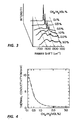
- Figure 3 as illustrated by A. Ono, T. Baba, H. Funamoto, A. Nishikawa, "Thermal Conductivity of Diamond Films Synthesized by Microwave Plasma-CVD", Japanese Journal of Applied Physics, Vol.
- Figure 4 from A. Ono, T. Baba, H. Funamoto, A. Nishikawa, ibid., which illustrates the thermal conductivity of a number of diamond thin films prepared at various methane/hydrogen gas ratios, indicates the increase in the thermal conductivity of the film when lower methane/hydrogen gas ratios are used.
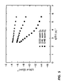
- Figures 5 and 6 indicate the impact of oxygen gas on the relative proportion of diamond-graphitic bonding within the thin film. As illustrated in Figure 5, which shows the electrical conductivity of diamond films as a function of temperature, the electrically insulating property of diamond is maximized, for a range of temperatures, when oxygen is introduced to the process at a rate of approximately 0.46 sccm.
- Figure 6 which illustrates the comparative Raman spectrographic responses of two diamond films, indicates the importance of the introduction of oxygen to the CVD process.
- the upper curve of Figure 6 represents the characterization of a film produced with an oxygen flow rate of 0.46 sccm, while the lower curve characterizes a film produced in the absence of oxygen in the CVD process.
- the relative proportions of the diamond versus the graphitic bonding peaks provide evidence of the predominance of tetrahedral, or diamond, bonding when the film is produced in the presence of oxygen.
- Production of acceptable diamond thin films has been achieved using oxygen flow rates in the range of 0.1 - 1.0 sccm, optimization of the flow rate is therefore, also dependent upon the methane/hydrogen gas ratio in conjunction with other process parameters.
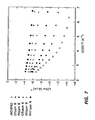
- the room temperature resistivity of polycrystalline diamond thin films is a strong function of the substrate temperature and exhibits a maximum at about 500 - 800 °C. This is consistent with the observation that the graphitic bonding in the film goes through a minimum in the same temperature range and the separate determination, from Figures 6 and 7, that the resistivity of the films correlates inversely with the graphitic content.
- the preferred temperature range for the fabrication of polycrystalline diamond MISFET transistors is therefore within this range, with optimization of the film at about 650 - 750 °C.
- Figure 8 illustrates the relative importance of boron doping to the resistivity of the diamond film as a function of operating temperature.
- the polycrystalline diamond film is observed to consistently exhibit a higher resistivity than that achievable by the intentional doping of the films with varying levels of boron. From Figure 8, it is apparent that the effective resistivity, and hence functionality of the polycrystalline diamond film as a field effect semiconductive layer, are optimized at low dopant or undoped concentrations of boron.
- a monovalent dopant such as lithium
- a monovalent dopant such as lithium
- the introduction of dopants is not intended to increase the conductivity of the film, but rather to counterbalance the effects caused by the presence of unintentional dopants within the polycrystalline diamond films.
- intentional dopants those introduced intentionally during the preparation of the thin film transistor, may be necessary to reduce the effects of the unintentional dopants that exist within the polycrystalline diamond film as produced. For this reason, the intentional dopant level will be optimally very small, or ideally non-existent, thereby rendering a polycrystalline diamond film with increased resistivity and therefore capable of exhibiting a maximum field effect response.
- the present invention is directed to a thin film field effect transistor made from a thin polycrystalline diamond film formed on one surface of a gate insulating film which has a gate electrode formed on the other surface thereof. Source and drain electrodes are formed on the other surface of the polycrystalline diamond film.
Landscapes
- Thin Film Transistor (AREA)
- Electrodes Of Semiconductors (AREA)
Applications Claiming Priority (2)
| Application Number | Priority Date | Filing Date | Title |
|---|---|---|---|
| US505754 | 1983-06-20 | ||
| US07/505,754 US5099296A (en) | 1990-04-06 | 1990-04-06 | Thin film transistor |
Publications (3)
| Publication Number | Publication Date |
|---|---|
| EP0450985A2 true EP0450985A2 (de) | 1991-10-09 |
| EP0450985A3 EP0450985A3 (en) | 1991-11-06 |
| EP0450985B1 EP0450985B1 (de) | 1995-03-15 |
Family
ID=24011692
Family Applications (1)
| Application Number | Title | Priority Date | Filing Date |
|---|---|---|---|
| EP91303046A Expired - Lifetime EP0450985B1 (de) | 1990-04-06 | 1991-04-05 | Dünnschichttransistor aus Diamant |
Country Status (4)
| Country | Link |
|---|---|
| US (1) | US5099296A (de) |
| EP (1) | EP0450985B1 (de) |
| JP (1) | JPH04225571A (de) |
| DE (1) | DE69108080T2 (de) |
Cited By (1)
| Publication number | Priority date | Publication date | Assignee | Title |
|---|---|---|---|---|
| GB2252202A (en) * | 1991-01-28 | 1992-07-29 | Kobe Steel Ltd | Semiconducting polycrystalline diamond electronic devices employing an insulating diamond layer |
Families Citing this family (15)
| Publication number | Priority date | Publication date | Assignee | Title |
|---|---|---|---|---|
| GB9021689D0 (en) * | 1990-10-05 | 1990-11-21 | De Beers Ind Diamond | Diamond neutron detector |
| JP3255960B2 (ja) * | 1991-09-30 | 2002-02-12 | 株式会社神戸製鋼所 | 冷陰極エミッタ素子 |
| JPH05299705A (ja) * | 1992-04-16 | 1993-11-12 | Kobe Steel Ltd | ダイヤモンド薄膜電子デバイス及びその製造方法 |
| USH1287H (en) | 1992-06-16 | 1994-02-01 | The United States Of America As Represented By The Secretary Of The Navy | Ion implanted diamond metal-insulator-semiconductor field effect transistor |
| US5300188A (en) * | 1992-11-13 | 1994-04-05 | Kobe Development Corp. | Process for making substantially smooth diamond |
| JP3334286B2 (ja) * | 1993-09-30 | 2002-10-15 | ソニー株式会社 | ダイアモンド半導体の製造方法 |
| US5738731A (en) * | 1993-11-19 | 1998-04-14 | Mega Chips Corporation | Photovoltaic device |
| JP3501552B2 (ja) * | 1995-06-29 | 2004-03-02 | 株式会社神戸製鋼所 | ダイヤモンド電極 |
| US5653800A (en) * | 1995-08-03 | 1997-08-05 | Eneco, Inc. | Method for producing N-type semiconducting diamond |
| US6011356A (en) * | 1998-04-30 | 2000-01-04 | St. Clair Intellectual Property Consultants, Inc. | Flat surface emitter for use in field emission display devices |
| CN1265465C (zh) | 2001-04-04 | 2006-07-19 | 三菱电机株式会社 | 半导体器件 |
| CA2419709C (en) * | 2002-02-26 | 2008-09-23 | Smith International, Inc. | Semiconductive polycrystalline diamond |
| US7402835B2 (en) * | 2002-07-18 | 2008-07-22 | Chevron U.S.A. Inc. | Heteroatom-containing diamondoid transistors |
| JP2013232600A (ja) * | 2012-05-01 | 2013-11-14 | Denso Corp | 熱電子発電素子 |
| US10418475B2 (en) * | 2016-11-28 | 2019-09-17 | Arizona Board Of Regents On Behalf Of Arizona State University | Diamond based current aperture vertical transistor and methods of making and using the same |
Family Cites Families (11)
| Publication number | Priority date | Publication date | Assignee | Title |
|---|---|---|---|---|
| US4265990A (en) * | 1977-05-04 | 1981-05-05 | Xerox Corporation | Imaging system with a diamine charge transport material in a polycarbonate resin |
| US4546009A (en) * | 1979-10-01 | 1985-10-08 | Exxon Research Engineering Co | High-mobility amorphous silicon displaying non-dispersive transport properties |
| JPS58141572A (ja) * | 1982-02-18 | 1983-08-22 | Seiko Epson Corp | 半導体装置 |
| JPS59213126A (ja) * | 1983-05-19 | 1984-12-03 | Sumitomo Electric Ind Ltd | ダイヤモンド半導体素子の製造法 |
| US4571447A (en) * | 1983-06-24 | 1986-02-18 | Prins Johan F | Photovoltaic cell of semi-conducting diamond |
| JPS60221395A (ja) * | 1984-04-19 | 1985-11-06 | Yoshio Imai | ダイヤモンド薄膜の製造方法 |
| JPS60246627A (ja) * | 1984-05-21 | 1985-12-06 | Sumitomo Electric Ind Ltd | ダイヤモンド半導体素子 |
| US4849797A (en) * | 1987-01-23 | 1989-07-18 | Hosiden Electronics Co., Ltd. | Thin film transistor |
| DE3725700A1 (de) * | 1987-08-03 | 1989-02-16 | Siemens Ag | Neues halbleitergrundmaterial |
| GB8812216D0 (en) * | 1988-05-24 | 1988-06-29 | Jones B L | Diamond transistor method of manufacture thereof |
| US4925701A (en) * | 1988-05-27 | 1990-05-15 | Xerox Corporation | Processes for the preparation of polycrystalline diamond films |
-
1990
- 1990-04-06 US US07/505,754 patent/US5099296A/en not_active Expired - Fee Related
-
1991
- 1991-03-29 JP JP3066932A patent/JPH04225571A/ja active Pending
- 1991-04-05 DE DE69108080T patent/DE69108080T2/de not_active Expired - Fee Related
- 1991-04-05 EP EP91303046A patent/EP0450985B1/de not_active Expired - Lifetime
Cited By (2)
| Publication number | Priority date | Publication date | Assignee | Title |
|---|---|---|---|---|
| GB2252202A (en) * | 1991-01-28 | 1992-07-29 | Kobe Steel Ltd | Semiconducting polycrystalline diamond electronic devices employing an insulating diamond layer |
| GB2252202B (en) * | 1991-01-28 | 1994-12-14 | Kobe Steel Ltd | Semiconducting polycrystalline diamond electronic devices employing an insulating diamond layer and method of making same |
Also Published As
| Publication number | Publication date |
|---|---|
| EP0450985A3 (en) | 1991-11-06 |
| US5099296A (en) | 1992-03-24 |
| EP0450985B1 (de) | 1995-03-15 |
| DE69108080T2 (de) | 1995-11-09 |
| JPH04225571A (ja) | 1992-08-14 |
| DE69108080D1 (de) | 1995-04-20 |
Similar Documents
| Publication | Publication Date | Title |
|---|---|---|
| EP0450985B1 (de) | Dünnschichttransistor aus Diamant | |
| US5170231A (en) | Silicon carbide field-effect transistor with improved breakdown voltage and low leakage current | |
| US6458699B1 (en) | Methods of forming a contact to a substrate | |
| US4814842A (en) | Thin film transistor utilizing hydrogenated polycrystalline silicon | |
| US4409605A (en) | Amorphous semiconductors equivalent to crystalline semiconductors | |
| US4741964A (en) | Structure containing hydrogenated amorphous silicon and process | |
| EP0322161B1 (de) | Siliciumcarbidsperre zwischen einem Siliciumsubstrat und einer Metallschicht | |
| EP0276002A2 (de) | Dünnschichttransistor | |
| GB2147316A (en) | A method of making p-doped silicon films and devices made therefrom | |
| US7923322B2 (en) | Method of forming a capacitor | |
| WO2009129391A2 (en) | Low temperature thin film transistor process, device property, and device stability improvement | |
| IE54526B1 (en) | Current enhanced photovoltaic device | |
| EP0061923A1 (de) | Halbleiteranordnung mit einer dünnen polykristallinen Schicht | |
| GB2124826A (en) | Amorphous semiconductor materials | |
| CA1153480A (en) | Thin film transistor | |
| US5216264A (en) | Silicon carbide MOS type field-effect transistor with at least one of the source and drain regions is formed by the use of a schottky contact | |
| JP2003298077A (ja) | 太陽電池 | |
| JP3117563B2 (ja) | ダイヤモンド薄膜電界効果トランジスタ | |
| Futagi et al. | Highly conductive and wide optical band gap n‐type μc‐SiC prepared by electron cyclotron resonance plasma‐enhanced chemical vapor deposition | |
| US4839312A (en) | Fluorinated precursors from which to fabricate amorphous semiconductor material | |
| CN117238914B (zh) | 一种集成SBD的SiC器件及制备方法 | |
| JP2523679B2 (ja) | 薄膜トランジスタおよびその製造方法 | |
| JPH0521798A (ja) | 薄膜トランジスタ | |
| JPH0554692B2 (de) | ||
| JPH0435019A (ja) | 薄膜トランジスター |
Legal Events
| Date | Code | Title | Description |
|---|---|---|---|
| PUAI | Public reference made under article 153(3) epc to a published international application that has entered the european phase |
Free format text: ORIGINAL CODE: 0009012 |
|
| PUAL | Search report despatched |
Free format text: ORIGINAL CODE: 0009013 |
|
| AK | Designated contracting states |
Kind code of ref document: A2 Designated state(s): DE FR GB |
|
| AK | Designated contracting states |
Kind code of ref document: A3 Designated state(s): DE FR GB |
|
| 17P | Request for examination filed |
Effective date: 19920429 |
|
| 17Q | First examination report despatched |
Effective date: 19940422 |
|
| GRAA | (expected) grant |
Free format text: ORIGINAL CODE: 0009210 |
|
| AK | Designated contracting states |
Kind code of ref document: B1 Designated state(s): DE FR GB |
|
| REF | Corresponds to: |
Ref document number: 69108080 Country of ref document: DE Date of ref document: 19950420 |
|
| ET | Fr: translation filed | ||
| PLBE | No opposition filed within time limit |
Free format text: ORIGINAL CODE: 0009261 |
|
| STAA | Information on the status of an ep patent application or granted ep patent |
Free format text: STATUS: NO OPPOSITION FILED WITHIN TIME LIMIT |
|
| 26N | No opposition filed | ||
| REG | Reference to a national code |
Ref country code: GB Ref legal event code: IF02 |
|
| REG | Reference to a national code |
Ref country code: GB Ref legal event code: 746 Effective date: 20050404 |
|
| PGFP | Annual fee paid to national office [announced via postgrant information from national office to epo] |
Ref country code: DE Payment date: 20070329 Year of fee payment: 17 |
|
| PGFP | Annual fee paid to national office [announced via postgrant information from national office to epo] |
Ref country code: GB Payment date: 20070404 Year of fee payment: 17 |
|
| PGFP | Annual fee paid to national office [announced via postgrant information from national office to epo] |
Ref country code: FR Payment date: 20070411 Year of fee payment: 17 |
|
| GBPC | Gb: european patent ceased through non-payment of renewal fee |
Effective date: 20080405 |
|
| PG25 | Lapsed in a contracting state [announced via postgrant information from national office to epo] |
Ref country code: DE Free format text: LAPSE BECAUSE OF NON-PAYMENT OF DUE FEES Effective date: 20081101 |
|
| REG | Reference to a national code |
Ref country code: FR Ref legal event code: ST Effective date: 20081231 |
|
| PG25 | Lapsed in a contracting state [announced via postgrant information from national office to epo] |
Ref country code: FR Free format text: LAPSE BECAUSE OF NON-PAYMENT OF DUE FEES Effective date: 20080430 |
|
| PG25 | Lapsed in a contracting state [announced via postgrant information from national office to epo] |
Ref country code: GB Free format text: LAPSE BECAUSE OF NON-PAYMENT OF DUE FEES Effective date: 20080405 |