EP0449319A2 - Schaltung zur Mikrofoniereduzierung - Google Patents
Schaltung zur Mikrofoniereduzierung Download PDFInfo
- Publication number
- EP0449319A2 EP0449319A2 EP91105092A EP91105092A EP0449319A2 EP 0449319 A2 EP0449319 A2 EP 0449319A2 EP 91105092 A EP91105092 A EP 91105092A EP 91105092 A EP91105092 A EP 91105092A EP 0449319 A2 EP0449319 A2 EP 0449319A2
- Authority
- EP
- European Patent Office
- Prior art keywords
- circuit
- capacitor
- voltage
- microphony
- capacitors
- Prior art date
- Legal status (The legal status is an assumption and is not a legal conclusion. Google has not performed a legal analysis and makes no representation as to the accuracy of the status listed.)
- Granted
Links
Images

Classifications
-
- H—ELECTRICITY
- H03—ELECTRONIC CIRCUITRY
- H03L—AUTOMATIC CONTROL, STARTING, SYNCHRONISATION OR STABILISATION OF GENERATORS OF ELECTRONIC OSCILLATIONS OR PULSES
- H03L7/00—Automatic control of frequency or phase; Synchronisation
- H03L7/06—Automatic control of frequency or phase; Synchronisation using a reference signal applied to a frequency- or phase-locked loop
- H03L7/08—Details of the phase-locked loop
- H03L7/085—Details of the phase-locked loop concerning mainly the frequency- or phase-detection arrangement including the filtering or amplification of its output signal
- H03L7/093—Details of the phase-locked loop concerning mainly the frequency- or phase-detection arrangement including the filtering or amplification of its output signal using special filtering or amplification characteristics in the loop
Definitions
- the invention relates to a method for reducing microphony in a circuit which includes ceramic surface-mounted capacitors.
- the invention also relates to a circuit by means of which the method according to the invention is implemented.
- Microphony of a ceramic capacitor means that the voltage between the capacitor terminals changes under mechanical action.
- the mechanical action may consist of impacts or vibration, causing deformation of the capacitor and appearing, for example, in a radio telephone which is portable or installed in an automobile.
- Efforts have been made to reduce microphony by placing the critical capacitors in a location where their fastening is as firm as possible, i.e. where their deformation is minimal. Special attention must also be paid to the fastening of the printed circuit board which serves as the substrate for the surface-mounted capacitor.
- the object of the invention is thus to find for the problem a new solution by which the effects of the microphony of ceramic surface-mounted capacitors are reduced.
- a method is presented in the characterizing clause of Claim 1 as a solution to this problem. If the direct voltage effective across the capacitor is eliminated, microphony does not substantially cause non-desirable interference voltage.
- Embodiments of the invention are presented in the non-independent claims.
- the loop filter is a filter coupled between the phase comparator and the VCO, here a second-degree active filter by means of which the operating parameters of the loop are determined at the frequency and time levels (e.g. settling time, modulation response).
- the loop filter functions within the audio frequency range, the typical cut-off frequency of the low-pass stage being approx. 200 Hertz. With practical component values, this usually leads to the use of components in an order of magnitude of 10 - 47 nF. Implemented by the surface-mounting technique, ceramic components of this magnitude are quite microphonic. Passive-stage capacitors connected after the active loop filter are particularly prone to develop microphony, since even an interference voltage of 1 millivolt in the VCO control line corresponds the highest possible speech volume as the modulation of the transmission signal of a mobile telephone.
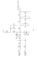
- Figure 1 depicts the circuit diagram of the loop filter of the frequency synthesizer used in a radio telephone. This circuit has been implemented using surface-mounted components. In the loop filter the ceramic surface-mounted capacitors C30 - C33 (22 nF) to the right of the transistor pair V20 are coupled between the signal lead and the ground. When the circuit board is subjected to an impact, owing to the microphony of the capacitors an interference voltage with a strongly varying amplitude is produced in the circuit (in the output VCO Control Voltage).
- the invention is based on an idea model of the production of a non-desirable, i.e. interference voltage: when a capacitor is bent mechanically, its capacitance value changes. Since the electric charge of the capacitor remains unchanged (electrons do not disappear), from this follows between the capacitor terminals a voltage change proportional to the change in the component value, i.e. the capacitance.
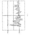
- Figure 2 depicts an oscillogram which shows the strong impact response (oscillation of the voltage) of the capacitor.
- Channel 2 (indicated by CH2 gnd) has the interference voltage caused by the capacitor coupled according to the principle of Figure 1
- channel 1 indicated by CH1 gnd
- the ceramic piece capacitor e.g. C30
- the oscilloscope settings and test coupling amplifications were fully identical.
- the effect of the invention was verified, i.e. the reduction of the interference voltage, even to the extent that the arrangement according to the invention can be deemed to prevent substantially the production of an interference voltage due to capacitor microphony.
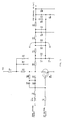
- the method according to the invention can be implemented by arranging a circuit which eliminates the direct voltage effective across ceramic capacitors.
- the loop filter circuit of Figure 1 is used as an example.
- the signal ground of the capacitors was separated from the actual ground potential by means of a tantalum capacitor.
- Figure 3 depicts a circuit like this, with a tantalum capacitor C40 (1 ⁇ F).
- microphony may appear on the ceramic capacitors C30 - C36 (22 nF).
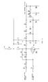
- Figure 5 finally depicts a loop filter implemented using operational amplifiers.
- the operational amplifiers N10A and N10B are coupled in such a manner that they actively cancel any possible direct-voltage differential V1-V2.
- the apparent ground potential is formed by a tantalum capacitor C40 (10 ⁇ F).
- FIG. 3 A comparison of Figures 3 - 5 to the loop filter according to Figure 1 shows that they have certain additional components due to practical circuit design.
- the components essential from the viewpoint of the invention were mentioned above in connection with the figures. It is hardly necessary to describe the operation of the circuits of Figures 1, 3 - 5 in greater detail in this context, since it is evident for an expert in the art and does not as such relate to the application of the invention.
- the method according to the invention can also be implemented in a plurality of other ways which may occur to an expert in the art upon reading this specification.
- the described loop filter of a frequency synthesizer is only one example of the circuits in which the method according to the invention can be applied for reducing microphony.
Landscapes
- Filters And Equalizers (AREA)
- Reverberation, Karaoke And Other Acoustics (AREA)
- Networks Using Active Elements (AREA)
- Measurement Of Velocity Or Position Using Acoustic Or Ultrasonic Waves (AREA)
- Ultra Sonic Daignosis Equipment (AREA)
- Developing Agents For Electrophotography (AREA)
- Control Of El Displays (AREA)
- Circuit For Audible Band Transducer (AREA)
- Details Of Audible-Bandwidth Transducers (AREA)
- Stabilization Of Oscillater, Synchronisation, Frequency Synthesizers (AREA)
Applications Claiming Priority (2)
| Application Number | Priority Date | Filing Date | Title |
|---|---|---|---|
| FI901583A FI88829C (fi) | 1990-03-29 | 1990-03-29 | Foerfarande och krets foer reducering av mikrofoni |
| FI901583 | 1990-03-29 |
Publications (3)
| Publication Number | Publication Date |
|---|---|
| EP0449319A2 true EP0449319A2 (de) | 1991-10-02 |
| EP0449319A3 EP0449319A3 (de) | 1991-10-16 |
| EP0449319B1 EP0449319B1 (de) | 1995-10-04 |
Family
ID=8530155
Family Applications (1)
| Application Number | Title | Priority Date | Filing Date |
|---|---|---|---|
| EP91105092A Expired - Lifetime EP0449319B1 (de) | 1990-03-29 | 1991-03-28 | Schaltung zur Mikrofoniereduzierung |
Country Status (7)
| Country | Link |
|---|---|
| US (1) | US5153468A (de) |
| EP (1) | EP0449319B1 (de) |
| JP (1) | JPH04348608A (de) |
| AT (1) | ATE128798T1 (de) |
| CA (1) | CA2039363A1 (de) |
| DE (1) | DE69113498T2 (de) |
| FI (1) | FI88829C (de) |
Families Citing this family (4)
| Publication number | Priority date | Publication date | Assignee | Title |
|---|---|---|---|---|
| GB2313001B (en) * | 1996-05-07 | 2000-11-01 | Nokia Mobile Phones Ltd | Frequency modulation using a phase-locked loop |
| GB2317512B (en) * | 1996-09-12 | 2001-01-24 | Nokia Mobile Phones Ltd | Frequency modulation using a phase-locked loop |
| FI105426B (fi) * | 1998-05-29 | 2000-08-15 | Nokia Mobile Phones Ltd | Digitaalinen vaihevertailija ilman kuollutta aluetta |
| KR100554137B1 (ko) * | 1998-09-17 | 2006-05-12 | 주식회사 하이닉스반도체 | 필터 회로 |
Family Cites Families (7)
| Publication number | Priority date | Publication date | Assignee | Title |
|---|---|---|---|---|
| DE2443581B2 (de) * | 1974-09-12 | 1979-11-29 | Blaupunkt-Werke Gmbh, 3200 Hildesheim | Schaltungsanordnung zur Detektion von Störsignalanteilen |
| DE2734112C2 (de) * | 1977-07-28 | 1982-11-11 | Siemens AG, 1000 Berlin und 8000 München | Verstärkende Zweikreis-Bandfilteranordnung |
| US4392254A (en) * | 1980-09-29 | 1983-07-05 | Motorola Inc. | Mechanical tuner with microphonics elimination circuitry |
| US4752749A (en) * | 1986-12-22 | 1988-06-21 | Rockwell International Corporation | Fast response tuner |
| FR2612707B1 (fr) * | 1987-03-17 | 1989-05-26 | Thomson Semiconducteurs | Oscillateur hyperfrequence integre dans un guide d'ondes |
| JPH0770975B2 (ja) * | 1988-01-26 | 1995-07-31 | シャープ株式会社 | 波形変換回路 |
| US4994774A (en) * | 1988-02-19 | 1991-02-19 | U.S. Philips Corporation | Integrated low-pass filter arrangement |
-
1990
- 1990-03-29 FI FI901583A patent/FI88829C/fi not_active IP Right Cessation
-
1991
- 1991-03-27 US US07/676,199 patent/US5153468A/en not_active Expired - Lifetime
- 1991-03-28 AT AT91105092T patent/ATE128798T1/de active
- 1991-03-28 DE DE69113498T patent/DE69113498T2/de not_active Expired - Fee Related
- 1991-03-28 CA CA002039363A patent/CA2039363A1/en not_active Abandoned
- 1991-03-28 EP EP91105092A patent/EP0449319B1/de not_active Expired - Lifetime
- 1991-03-29 JP JP3089273A patent/JPH04348608A/ja active Pending
Also Published As
| Publication number | Publication date |
|---|---|
| ATE128798T1 (de) | 1995-10-15 |
| EP0449319B1 (de) | 1995-10-04 |
| CA2039363A1 (en) | 1991-09-30 |
| FI901583L (fi) | 1991-09-30 |
| US5153468A (en) | 1992-10-06 |
| FI88829C (fi) | 1993-07-12 |
| DE69113498D1 (de) | 1995-11-09 |
| JPH04348608A (ja) | 1992-12-03 |
| DE69113498T2 (de) | 1996-04-25 |
| FI88829B (fi) | 1993-03-31 |
| EP0449319A3 (de) | 1991-10-16 |
| FI901583A0 (fi) | 1990-03-29 |
Similar Documents
| Publication | Publication Date | Title |
|---|---|---|
| US5399996A (en) | Circuit and method for minimizing electromagnetic emissions | |
| US6163207A (en) | Integrator-filter circuit | |
| AU706217B2 (en) | A loop filter of a phase-locked loop | |
| US20110170698A1 (en) | Frequency modulator and fm transmission circuit using the same | |
| US5144264A (en) | Wideband voltage controlled oscillator having open loop gain compensation | |
| US9859843B2 (en) | Device for controlling a capacitor having an adjustable capacitance | |
| CN1951016A (zh) | 用于压控频率发生器中的干扰补偿的方法和装置 | |
| US6792121B2 (en) | Audio signal amplifier circuit and portable telephone set and portable electronic device using the same audio signal amplifier circuit | |
| EP0449319A2 (de) | Schaltung zur Mikrofoniereduzierung | |
| KR19990077877A (ko) | 주파수 신시사이저를 포함하는 전자장치 및 주파수 신시사이저를 제어하는 방법 | |
| JP4685862B2 (ja) | 干渉に堅固な水晶発振器用バッファ | |
| EP1485993B1 (de) | R.f. ausgangsleistungsreglung | |
| EP0522425B1 (de) | Einrichtung zur Erzeugung eines Signals | |
| JPH09190229A (ja) | 電気通信端末装置および集積回路 | |
| CN114900158B (zh) | 松弛振荡器及其自校准方法 | |
| US4296381A (en) | Distortion reduction circuit for an inverting feedback amplifier | |
| US20080024239A1 (en) | Coil-less overtone crystal oscillator | |
| KR100338643B1 (ko) | 위상동기루프에서 위상잡음을 감소시키기 위한 장치 | |
| EP3614565A1 (de) | Filter mit gleichstrompegelschiebung und zugehöriger phasenregelkreis | |
| US7573414B2 (en) | Maintaining a reference voltage constant against load variations | |
| JP2004146882A (ja) | デジタル制御温度補償基準発振器およびそれを用いた電子装置 | |
| JP2000284836A (ja) | 安定化電源回路 | |
| JP3366483B2 (ja) | フィルタ回路 | |
| US7667553B2 (en) | Frequency modulator using PLL | |
| JPH05129833A (ja) | 発振回路 |
Legal Events
| Date | Code | Title | Description |
|---|---|---|---|
| PUAI | Public reference made under article 153(3) epc to a published international application that has entered the european phase |
Free format text: ORIGINAL CODE: 0009012 |
|
| PUAL | Search report despatched |
Free format text: ORIGINAL CODE: 0009013 |
|
| AK | Designated contracting states |
Kind code of ref document: A2 Designated state(s): AT BE CH DE DK ES FR GB GR IT LI LU NL SE |
|
| AK | Designated contracting states |
Kind code of ref document: A3 Designated state(s): AT BE CH DE DK ES FR GB GR IT LI LU NL SE |
|
| 17P | Request for examination filed |
Effective date: 19920402 |
|
| 17Q | First examination report despatched |
Effective date: 19920805 |
|
| GRAA | (expected) grant |
Free format text: ORIGINAL CODE: 0009210 |
|
| AK | Designated contracting states |
Kind code of ref document: B1 Designated state(s): AT BE CH DE DK ES FR GB GR IT LI LU NL SE |
|
| PG25 | Lapsed in a contracting state [announced via postgrant information from national office to epo] |
Ref country code: IT Free format text: LAPSE BECAUSE OF FAILURE TO SUBMIT A TRANSLATION OF THE DESCRIPTION OR TO PAY THE FEE WITHIN THE PRE;WARNING: LAPSES OF ITALIAN PATENTS WITH EFFECTIVE DATE BEFORE 2007 MAY HAVE OCCURRED AT ANY TIME BEFORE 2007. THE CORRECT EFFECTIVE DATE MAY BE DIFFERENT FROM THE ONE RECORDED.SCRIBED TIME-LIMIT Effective date: 19951004 Ref country code: AT Effective date: 19951004 Ref country code: CH Effective date: 19951004 Ref country code: DK Effective date: 19951004 Ref country code: ES Free format text: THE PATENT HAS BEEN ANNULLED BY A DECISION OF A NATIONAL AUTHORITY Effective date: 19951004 Ref country code: GR Free format text: LAPSE BECAUSE OF FAILURE TO SUBMIT A TRANSLATION OF THE DESCRIPTION OR TO PAY THE FEE WITHIN THE PRESCRIBED TIME-LIMIT Effective date: 19951004 Ref country code: LI Effective date: 19951004 Ref country code: FR Effective date: 19951004 Ref country code: BE Effective date: 19951004 Ref country code: NL Free format text: LAPSE BECAUSE OF FAILURE TO SUBMIT A TRANSLATION OF THE DESCRIPTION OR TO PAY THE FEE WITHIN THE PRESCRIBED TIME-LIMIT Effective date: 19951004 |
|
| REF | Corresponds to: |
Ref document number: 128798 Country of ref document: AT Date of ref document: 19951015 Kind code of ref document: T |
|
| REF | Corresponds to: |
Ref document number: 69113498 Country of ref document: DE Date of ref document: 19951109 |
|
| PG25 | Lapsed in a contracting state [announced via postgrant information from national office to epo] |
Ref country code: SE Effective date: 19960104 |
|
| EN | Fr: translation not filed | ||
| NLV1 | Nl: lapsed or annulled due to failure to fulfill the requirements of art. 29p and 29m of the patents act | ||
| PG25 | Lapsed in a contracting state [announced via postgrant information from national office to epo] |
Ref country code: LU Free format text: LAPSE BECAUSE OF NON-PAYMENT OF DUE FEES Effective date: 19960331 |
|
| REG | Reference to a national code |
Ref country code: CH Ref legal event code: PL |
|
| PLBE | No opposition filed within time limit |
Free format text: ORIGINAL CODE: 0009261 |
|
| STAA | Information on the status of an ep patent application or granted ep patent |
Free format text: STATUS: NO OPPOSITION FILED WITHIN TIME LIMIT |
|
| 26N | No opposition filed | ||
| REG | Reference to a national code |
Ref country code: GB Ref legal event code: IF02 |
|
| REG | Reference to a national code |
Ref country code: GB Ref legal event code: 732E |
|
| PGFP | Annual fee paid to national office [announced via postgrant information from national office to epo] |
Ref country code: GB Payment date: 20040324 Year of fee payment: 14 |
|
| PGFP | Annual fee paid to national office [announced via postgrant information from national office to epo] |
Ref country code: DE Payment date: 20040408 Year of fee payment: 14 |
|
| PG25 | Lapsed in a contracting state [announced via postgrant information from national office to epo] |
Ref country code: GB Free format text: LAPSE BECAUSE OF NON-PAYMENT OF DUE FEES Effective date: 20050328 |
|
| PG25 | Lapsed in a contracting state [announced via postgrant information from national office to epo] |
Ref country code: DE Free format text: LAPSE BECAUSE OF NON-PAYMENT OF DUE FEES Effective date: 20051001 |
|
| GBPC | Gb: european patent ceased through non-payment of renewal fee |
Effective date: 20050328 |