EP0448735A1 - Procédé pour l'exposition des bords de plaquettes semi-conductrices - Google Patents
Procédé pour l'exposition des bords de plaquettes semi-conductrices Download PDFInfo
- Publication number
- EP0448735A1 EP0448735A1 EP90105588A EP90105588A EP0448735A1 EP 0448735 A1 EP0448735 A1 EP 0448735A1 EP 90105588 A EP90105588 A EP 90105588A EP 90105588 A EP90105588 A EP 90105588A EP 0448735 A1 EP0448735 A1 EP 0448735A1
- Authority
- EP
- European Patent Office
- Prior art keywords
- wafer
- exposure
- photoresist
- peripheral part
- exposing
- Prior art date
- Legal status (The legal status is an assumption and is not a legal conclusion. Google has not performed a legal analysis and makes no representation as to the accuracy of the status listed.)
- Granted
Links
Images

Classifications
-
- G—PHYSICS
- G03—PHOTOGRAPHY; CINEMATOGRAPHY; ANALOGOUS TECHNIQUES USING WAVES OTHER THAN OPTICAL WAVES; ELECTROGRAPHY; HOLOGRAPHY
- G03F—PHOTOMECHANICAL PRODUCTION OF TEXTURED OR PATTERNED SURFACES, e.g. FOR PRINTING, FOR PROCESSING OF SEMICONDUCTOR DEVICES; MATERIALS THEREFOR; ORIGINALS THEREFOR; APPARATUS SPECIALLY ADAPTED THEREFOR
- G03F7/00—Photomechanical, e.g. photolithographic, production of textured or patterned surfaces, e.g. printing surfaces; Materials therefor, e.g. comprising photoresists; Apparatus specially adapted therefor
- G03F7/20—Exposure; Apparatus therefor
- G03F7/2022—Multi-step exposure, e.g. hybrid; backside exposure; blanket exposure, e.g. for image reversal; edge exposure, e.g. for edge bead removal; corrective exposure
- G03F7/2026—Multi-step exposure, e.g. hybrid; backside exposure; blanket exposure, e.g. for image reversal; edge exposure, e.g. for edge bead removal; corrective exposure for the removal of unwanted material, e.g. image or background correction
- G03F7/2028—Multi-step exposure, e.g. hybrid; backside exposure; blanket exposure, e.g. for image reversal; edge exposure, e.g. for edge bead removal; corrective exposure for the removal of unwanted material, e.g. image or background correction of an edge bead on wafers
-
- G—PHYSICS
- G03—PHOTOGRAPHY; CINEMATOGRAPHY; ANALOGOUS TECHNIQUES USING WAVES OTHER THAN OPTICAL WAVES; ELECTROGRAPHY; HOLOGRAPHY
- G03F—PHOTOMECHANICAL PRODUCTION OF TEXTURED OR PATTERNED SURFACES, e.g. FOR PRINTING, FOR PROCESSING OF SEMICONDUCTOR DEVICES; MATERIALS THEREFOR; ORIGINALS THEREFOR; APPARATUS SPECIALLY ADAPTED THEREFOR
- G03F7/00—Photomechanical, e.g. photolithographic, production of textured or patterned surfaces, e.g. printing surfaces; Materials therefor, e.g. comprising photoresists; Apparatus specially adapted therefor
- G03F7/16—Coating processes; Apparatus therefor
- G03F7/162—Coating on a rotating support, e.g. using a whirler or a spinner
Definitions
- This invention relates to a method of exposing a peripheral part of wafer which is used for a fine pattern formation process in the production of ICs, LSIs or other electronics elements. More particulary, this invention relates to removing, in a development step, an unnecessary portion of a photoresist coated on a semiconductor substrate, typically a silicon wafer, or a substrate consisting of a dielectric, a metal or an insulator.
- a photoresist pattern is formed by coating a photoresist on a silicon wafer or the like and exposing and developing the coated photoresist.
- the photoresist pattern thus formed is used as a mask to effect ion implantation, etching, lifting-off and other steps.
- the photoresist is coated by spin coating.
- the wafer is spun while pouring photoresist onto the center position of the right side of the wafer, and the poured photoresist is coated on the wafer by centrifugal forces.
- the photoresist gets off a peripheral part of the wafer and is brought to the wrong side of the wafer.
- Fig.2 is a cross sectional view showing photoresist coated on a wafer.
- reference numeral 1 designates a wafer, 1p a peripheral part of wafer, 1a a photoresist portion on a pattern formation part of the wafer, 1b a photoresist portion on a peripheral part 1p, and 1c a photoresist portion brought to the wrong side of the wafer 1 from the edge thereof.
- the photoresist portion 1c brought to the back side of the wafer is not illuminated in an exposure step for pattern formation, and if it is a positive photoresist, it remains after the development.
- Fig.3 is a typical view showing a circuit pattern formed by exposure on the wafer.
- Each area labeled T corresponds to one circuit pattern.
- a correct circuit pattern can not be formed in many cases, or it can be formed with a inferior yield.
- the photoresist portion 1b on a peripheral part of wafer is substantially unnecessary in the circuit pattern formation. Even if the peripheral part of wafer is exposed by a stepper, the photoresist remains unnecessarily after the development.
- the remaining of unnecessary photoresist coated on the peripheral part and brought to the wrong side of the wafer gives rise to the following problem.
- the wafer with the photoresist coated is conveyed in various steps and by various systems or units.
- a peripheral part of the wafer thus is sometimes mechanically chucked and sometimes rubs a wall of wafer cassette or like wafer accommodation means.
- the unnecessary photoresist portion on the peripheral part of wafer is liable to be removed and re-attached to a pattern formation portion of wafer. In this case, correct pattern formation can no longer be obtained, thus reducing the yield.
- the solvent is sprayed on the wrong side of the peripheral part of wafer, solving the unnecessary photoresist.
- the photoresist 1c as shown in Fig.2 can be removed, the unnecessary photoresist 1b on the right side of the peripheral part of wafer can not be removed.
- the borderline between the unnecessary photoresist 1b on the peripheral part of wafer and photoresist 1a necessary for the pattern formation as a mask layer for a subsequent ion implantation process or the like, as shown in Fig.2, can be sharply and with high controllability, so that this method is superior to the solvent spray method.
- An object of the invention is to provide a method of exposing a peripheral part of wafer, which is free from generation of bubbles in the photoresist and also free from pattern defects and permits high yield and productivity to be obtained.
- the portions with bubbles are spattered when the wafer rubs a wall of wafer cassette or the like.
- the spattered photoresist is attached as "refuse" to the pattern formation part of the wafer to bring about the problem of pattern defects as noted above.
- the illumination intensity in a first exposure the illumination intensity is set to a low level so that gases generated in the photoresist material will not be concentrated in any area but are emitted gradually to the outside of the photoresist material. Thus, no bubbles are formed in the photoresist material.
- the illumination intensity can be increased without possibility of bubble formation because gases have been substantially emitted at the time of the first exposure.
- the turning speed of the wafer can be increased to shorten the exposure time.
- a peripheral part of the wafer to light guided by single optical fiber lightguide at a first illumination intensity while turning said wafer, exposing the same area to light guided by said single optical fiber lightguide at a second illumination intensity which is higher than the first illumination intensity while continuously turning said wafer again.
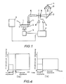
- Fig.1 schematically shows a main portion of an exposure apparatus for carrying out one embodiment of method of exposing a peripheral part of wafer according to the invention.
- reference numeral 1 designates a wafer
- 2 is a stage, on which the wafer 1 is set
- 3 is a stage drive system for turning the stage 2
- 4 is a system controller
- 5 is a wafer transport system for transporting the wafer 1 onto the stage 2
- 6 is a shutter actuator
- 7 is a shutter opened and closed by the shutter actuator 6
- 8 is a actuator of a light-reducing filter
- 9 is a light-reducing filter consisting of a metal mesh or the like to control the transmission of exposure light
- 10 is an optical fiber lightguide for guiding exposure light
- 11 is a light emission end of the optical fiber lightguide
- 12 is a plane mirror
- 13 is an oval light collector
- 14 is a discharge mercury lamp of short arc type (hereinafter referred to as lamp).
- rotary solenoids can be used for instance.
- the wafer transport system 5 transports the wafer 1 and sets it on the stage 2 according to a signal from the system controller 4.
- the stage 2, on which the wafer 1 is set chucks the wafer 1 by a vacuum chuck mechanism (not shown). Subsequently, the stage 2 is caused to turn, and the shutter 7 is opened by the shutter actuator 6 according to a signal from the system controller 4.
- the light-reducing filter 9 remains to be on an light path. Light from the lamp 14 is reduced by the filter 9 and emitted from the light emission end 11 of the optical fiber lightguide 10 to effect exposure of the peripheral part of the wafer 1. This exposure is done at reduced illumination intensity and is called first exposure. The first exposure continues while wafer 1 turns at an angle of 360 degree(1 cycle).
- the finish of first exposure is monitored by monitoring mechanism of turning angle(not shown, such as a counter for counting the number of pulses of a pulse motor for stage driving system 3, or a rotary encoder).
- monitoring mechanism of turning angle such as a counter for counting the number of pulses of a pulse motor for stage driving system 3, or a rotary encoder.
- system controller 4 Monitoring the wafer 1 turns at angle of 360 degree(finishing first exposure), system controller 4 sends a signal to filter actuator 8 to take away filter 9 from light path. Then the second exposure starts. From the first exposure to second exposure, turning motion of wafer 1 may be continued or stopped. If turning motion is stopped, the shutter 7 is used.
- the peripheral part of wafer 1 is exposed at higher illumination intensity because light-reducing filter 9 is taken away from light-path.
- the second exposure finishes after added 1 or more cycle of turning of wafer 1.
- the wafer 1 is transported from the stage 2 to a wafer cassette by the wafer transport system 5, and photoresist on the peripheral part of wafer is removed in development process by well-known means.
- Figs.4(a) and 4(b) show the illumination intensity for the first exposure and for the second and following exposures, respectively.
- the illumination intensity is set to 200 mW/cm2 in the first exposure and 2000 mW/cm2 in the second exposure.
- the illumination intensity in each exposure, exposure time and turning speed of course vary depending on the material of the photoresist.
- the exposure time for the first exposure can be reduced to about one-third. This is so because the gases produced by the exposure are quickly dispersed in the photoresist material and emitted to the outside thereof, while the photoresist is heated.
- the temperature in heating should be less than that of heat-resistance of the photoresist.
- each lightguide is set so that it may expose the peripheral part of wafer as shown in Fig.4 (a) or (b).
- the illumination intensity for the first exposure it is important to set the illumination intensity for the first exposure to be lower than that for the second exposure so that no bubbles will be formed in the photoresist in the first exposure. Therefore, for instance using two lightguides, illumination intensity of light form of one lightguide is set lower than another lightguide.
- illumination control means it is possible to control power supply to the lamp, or use a half mirror or filter in addition to the use of the light-reducing filter.
Priority Applications (2)
| Application Number | Priority Date | Filing Date | Title |
|---|---|---|---|
| EP19900105588 EP0448735B1 (fr) | 1990-03-23 | 1990-03-23 | Procédé pour l'exposition des bords de plaquettes semi-conductrices |
| DE1990631212 DE69031212T2 (de) | 1990-03-23 | 1990-03-23 | Randbelichtungsverfahren für Halbleiterscheiben |
Applications Claiming Priority (1)
| Application Number | Priority Date | Filing Date | Title |
|---|---|---|---|
| EP19900105588 EP0448735B1 (fr) | 1990-03-23 | 1990-03-23 | Procédé pour l'exposition des bords de plaquettes semi-conductrices |
Publications (2)
| Publication Number | Publication Date |
|---|---|
| EP0448735A1 true EP0448735A1 (fr) | 1991-10-02 |
| EP0448735B1 EP0448735B1 (fr) | 1997-08-06 |
Family
ID=8203803
Family Applications (1)
| Application Number | Title | Priority Date | Filing Date |
|---|---|---|---|
| EP19900105588 Expired - Lifetime EP0448735B1 (fr) | 1990-03-23 | 1990-03-23 | Procédé pour l'exposition des bords de plaquettes semi-conductrices |
Country Status (2)
| Country | Link |
|---|---|
| EP (1) | EP0448735B1 (fr) |
| DE (1) | DE69031212T2 (fr) |
Cited By (5)
| Publication number | Priority date | Publication date | Assignee | Title |
|---|---|---|---|---|
| WO2001082345A1 (fr) * | 2000-04-25 | 2001-11-01 | Advanced Micro Devices, Inc. | Systeme et procede d'eclairage d'un systeme de traitement de semi-conducteurs |
| WO2001084603A1 (fr) * | 2000-04-25 | 2001-11-08 | Advanced Micro Devices, Inc. | Dispositif d'eclairage pour systeme de traitement de semi-conducteurs et procede correspondant |
| WO2003091805A1 (fr) * | 2002-04-24 | 2003-11-06 | Obducat Ab | Procede, dispositif et produit de programme informatique pour lithographie |
| KR100787701B1 (ko) | 2002-04-24 | 2007-12-21 | 오브듀캇 아베 | 리소그래피용 방법, 장치 및 컴퓨터 판독가능한 기록 매체 |
| CN102479689A (zh) * | 2010-11-25 | 2012-05-30 | 拉碧斯半导体株式会社 | 基板处理系统及基板处理方法 |
Citations (4)
| Publication number | Priority date | Publication date | Assignee | Title |
|---|---|---|---|---|
| FR2151130A1 (en) * | 1971-09-01 | 1973-04-13 | Ibm | Photo mask mfr - eliminating defects by successive partial exposures |
| DE3314156A1 (de) * | 1983-04-19 | 1984-10-25 | Siemens AG, 1000 Berlin und 8000 München | Verfahren zur beschichtung scheibenfoermiger halbleitersubstrate mit photolack |
| DE3425761A1 (de) * | 1983-07-13 | 1985-02-07 | Fuji Photo Film Co., Ltd., Minami-Ashigara, Kanagawa | Seitenrandkopiervorrichtung |
| EP0325930A1 (fr) * | 1988-01-29 | 1989-08-02 | Ushio Denki | Procédé pour l'exposition des bords de plaquettes semi-conductrices |
-
1990
- 1990-03-23 EP EP19900105588 patent/EP0448735B1/fr not_active Expired - Lifetime
- 1990-03-23 DE DE1990631212 patent/DE69031212T2/de not_active Expired - Lifetime
Patent Citations (4)
| Publication number | Priority date | Publication date | Assignee | Title |
|---|---|---|---|---|
| FR2151130A1 (en) * | 1971-09-01 | 1973-04-13 | Ibm | Photo mask mfr - eliminating defects by successive partial exposures |
| DE3314156A1 (de) * | 1983-04-19 | 1984-10-25 | Siemens AG, 1000 Berlin und 8000 München | Verfahren zur beschichtung scheibenfoermiger halbleitersubstrate mit photolack |
| DE3425761A1 (de) * | 1983-07-13 | 1985-02-07 | Fuji Photo Film Co., Ltd., Minami-Ashigara, Kanagawa | Seitenrandkopiervorrichtung |
| EP0325930A1 (fr) * | 1988-01-29 | 1989-08-02 | Ushio Denki | Procédé pour l'exposition des bords de plaquettes semi-conductrices |
Non-Patent Citations (1)
| Title |
|---|
| PATENT ABSTRACTS OF JAPAN vol. 6, no. 264 (E-150)(1142) 23 December 1982, & JP-A-57 162336 (FUJITSU K.K.) 06 October 1982, * |
Cited By (11)
| Publication number | Priority date | Publication date | Assignee | Title |
|---|---|---|---|---|
| WO2001082345A1 (fr) * | 2000-04-25 | 2001-11-01 | Advanced Micro Devices, Inc. | Systeme et procede d'eclairage d'un systeme de traitement de semi-conducteurs |
| WO2001084603A1 (fr) * | 2000-04-25 | 2001-11-08 | Advanced Micro Devices, Inc. | Dispositif d'eclairage pour systeme de traitement de semi-conducteurs et procede correspondant |
| US6572252B1 (en) | 2000-04-25 | 2003-06-03 | Advanced Micro Devices, Inc. | System and method for illuminating a semiconductor processing system |
| US6632283B1 (en) | 2000-04-25 | 2003-10-14 | Advanced Micro Devices, Inc. | System and method for illuminating a semiconductor processing system |
| WO2003091805A1 (fr) * | 2002-04-24 | 2003-11-06 | Obducat Ab | Procede, dispositif et produit de programme informatique pour lithographie |
| CN1313884C (zh) * | 2002-04-24 | 2007-05-02 | 奥博杜卡特股份公司 | 光刻术的方法和装置 |
| KR100787701B1 (ko) | 2002-04-24 | 2007-12-21 | 오브듀캇 아베 | 리소그래피용 방법, 장치 및 컴퓨터 판독가능한 기록 매체 |
| US7468784B2 (en) | 2002-04-24 | 2008-12-23 | Obducat Ab | Method and device for forming optical or magnetic memory media or a template for the same |
| CN102479689A (zh) * | 2010-11-25 | 2012-05-30 | 拉碧斯半导体株式会社 | 基板处理系统及基板处理方法 |
| US20120135610A1 (en) * | 2010-11-25 | 2012-05-31 | Lapis Semiconductor Co., Ltd. | System and method for processing substrate |
| JP2012114259A (ja) * | 2010-11-25 | 2012-06-14 | Lapis Semiconductor Co Ltd | 基板処理システム及び基板処理方法 |
Also Published As
| Publication number | Publication date |
|---|---|
| EP0448735B1 (fr) | 1997-08-06 |
| DE69031212T2 (de) | 1998-01-29 |
| DE69031212D1 (de) | 1997-09-11 |
Similar Documents
| Publication | Publication Date | Title |
|---|---|---|
| US4899195A (en) | Method of exposing a peripheral part of wafer | |
| US6307620B1 (en) | Substrate holding apparatus, substrate transfer system, exposure apparatus, coating apparatus, method for making a device, and method for cleaning a substrate holding section | |
| US5204224A (en) | Method of exposing a peripheral part of a wafer | |
| US7417709B2 (en) | Method and apparatus for exposing semiconductor substrates | |
| EP0448735B1 (fr) | Procédé pour l'exposition des bords de plaquettes semi-conductrices | |
| GB2135793A (en) | Bilevel ultraviolet resist system for patterning substrates of high reflectivity | |
| KR100526527B1 (ko) | 포토마스크와 그를 이용한 마스크 패턴 형성 방법 | |
| JPH09293675A (ja) | 周辺露光装置 | |
| US6403285B1 (en) | Method for exposing semiconductor wafers in a manner that promotes radial processing uniformity | |
| JPH03242922A (ja) | ウエハ周辺露光方法及びウエハ周辺露光装置 | |
| JPH0750677B2 (ja) | ウエハ周辺露光方法 | |
| JP2610601B2 (ja) | ウエハ周辺露光装置 | |
| JPH0471224A (ja) | 露光装置 | |
| KR20040061442A (ko) | 기판의 에지 비드 제거장치 및 방법 | |
| KR200161792Y1 (ko) | 반도체 노광장치 | |
| KR100917822B1 (ko) | 웨이퍼 에지의 노광 장치 및 노광 방법 | |
| JPS61226750A (ja) | 半導体装置の製造方法 | |
| KR20040011792A (ko) | 기판 주변 노광 장치 | |
| KR20060122556A (ko) | 불순물 제거 기능을 가지는 반도체 장비 | |
| KR20050059622A (ko) | 웨이퍼 에지 노광 장치 | |
| KR19990031795A (ko) | 노광장치 및 이를 이용한 노광방법 | |
| JPS63301519A (ja) | レジストパタ−ン形成方法 | |
| JPH0341718A (ja) | 周辺露光装置 | |
| KR20020081927A (ko) | 반도체 웨이퍼의 에지 노광 방법 | |
| KR20020063964A (ko) | 웨이퍼 에지 노광장치 |
Legal Events
| Date | Code | Title | Description |
|---|---|---|---|
| PUAI | Public reference made under article 153(3) epc to a published international application that has entered the european phase |
Free format text: ORIGINAL CODE: 0009012 |
|
| AK | Designated contracting states |
Kind code of ref document: A1 Designated state(s): DE FR GB NL |
|
| 17P | Request for examination filed |
Effective date: 19920306 |
|
| 17Q | First examination report despatched |
Effective date: 19941117 |
|
| GRAG | Despatch of communication of intention to grant |
Free format text: ORIGINAL CODE: EPIDOS AGRA |
|
| GRAH | Despatch of communication of intention to grant a patent |
Free format text: ORIGINAL CODE: EPIDOS IGRA |
|
| GRAH | Despatch of communication of intention to grant a patent |
Free format text: ORIGINAL CODE: EPIDOS IGRA |
|
| GRAA | (expected) grant |
Free format text: ORIGINAL CODE: 0009210 |
|
| AK | Designated contracting states |
Kind code of ref document: B1 Designated state(s): DE FR GB NL |
|
| REF | Corresponds to: |
Ref document number: 69031212 Country of ref document: DE Date of ref document: 19970911 |
|
| ET | Fr: translation filed | ||
| PLBE | No opposition filed within time limit |
Free format text: ORIGINAL CODE: 0009261 |
|
| STAA | Information on the status of an ep patent application or granted ep patent |
Free format text: STATUS: NO OPPOSITION FILED WITHIN TIME LIMIT |
|
| 26N | No opposition filed | ||
| REG | Reference to a national code |
Ref country code: GB Ref legal event code: IF02 |
|
| PGFP | Annual fee paid to national office [announced via postgrant information from national office to epo] |
Ref country code: NL Payment date: 20090324 Year of fee payment: 20 |
|
| PGFP | Annual fee paid to national office [announced via postgrant information from national office to epo] |
Ref country code: GB Payment date: 20090324 Year of fee payment: 20 |
|
| PGFP | Annual fee paid to national office [announced via postgrant information from national office to epo] |
Ref country code: DE Payment date: 20090529 Year of fee payment: 20 |
|
| PGFP | Annual fee paid to national office [announced via postgrant information from national office to epo] |
Ref country code: FR Payment date: 20090318 Year of fee payment: 20 |
|
| REG | Reference to a national code |
Ref country code: NL Ref legal event code: V4 Effective date: 20100323 |
|
| REG | Reference to a national code |
Ref country code: GB Ref legal event code: PE20 Expiry date: 20100322 |
|
| PG25 | Lapsed in a contracting state [announced via postgrant information from national office to epo] |
Ref country code: GB Free format text: LAPSE BECAUSE OF EXPIRATION OF PROTECTION Effective date: 20100322 |
|
| PG25 | Lapsed in a contracting state [announced via postgrant information from national office to epo] |
Ref country code: NL Free format text: LAPSE BECAUSE OF EXPIRATION OF PROTECTION Effective date: 20100323 |
|
| PG25 | Lapsed in a contracting state [announced via postgrant information from national office to epo] |
Ref country code: DE Free format text: LAPSE BECAUSE OF EXPIRATION OF PROTECTION Effective date: 20100323 |