EP0448086A2 - Circuit de commande d'un tube image monochrome - Google Patents
Circuit de commande d'un tube image monochrome Download PDFInfo
- Publication number
- EP0448086A2 EP0448086A2 EP91104363A EP91104363A EP0448086A2 EP 0448086 A2 EP0448086 A2 EP 0448086A2 EP 91104363 A EP91104363 A EP 91104363A EP 91104363 A EP91104363 A EP 91104363A EP 0448086 A2 EP0448086 A2 EP 0448086A2
- Authority
- EP
- European Patent Office
- Prior art keywords
- voltage
- positive
- display
- negative
- amplifier
- Prior art date
- Legal status (The legal status is an assumption and is not a legal conclusion. Google has not performed a legal analysis and makes no representation as to the accuracy of the status listed.)
- Ceased
Links
Images

Classifications
-
- G—PHYSICS
- G09—EDUCATION; CRYPTOGRAPHY; DISPLAY; ADVERTISING; SEALS
- G09G—ARRANGEMENTS OR CIRCUITS FOR CONTROL OF INDICATING DEVICES USING STATIC MEANS TO PRESENT VARIABLE INFORMATION
- G09G1/00—Control arrangements or circuits, of interest only in connection with cathode-ray tube indicators; General aspects or details, e.g. selection emphasis on particular characters, dashed line or dotted line generation; Preprocessing of data
- G09G1/002—Intensity circuits
-
- H—ELECTRICITY
- H04—ELECTRIC COMMUNICATION TECHNIQUE
- H04N—PICTORIAL COMMUNICATION, e.g. TELEVISION
- H04N5/00—Details of television systems
- H04N5/44—Receiver circuitry for the reception of television signals according to analogue transmission standards
- H04N5/57—Control of contrast or brightness
Definitions
- the invention relates to a circuit arrangement for driving a monochrome picture tube with an image signal amplifier with adjustable gain, the input signal polarity of which can be switched to positive or negative representation, different reference potentials being provided for the amplified image signals.
- the first type of representation is referred to as a negative representation
- the control circuits of picture tubes can be switched to change the display type, for what the image signals supplied to the image signal amplifier can be negated or an existing negation can be canceled.
- this is a black potential in the case of a negative representation and a white potential in the case of a positive representation.
- the reference potential in the case of a negative display is set, for example, to a value at which the screen is currently changing to the black state. Starting from this reference potential, the gain of the image signal amplifier can be adjusted to change the contrast. The greater the gain is set, the greater the output voltage swing of the image signal amplifier, and thus the contrast between the background value and the displayed symbol, with the same image signal. If the display type is switched, the reference potential for the modulation of the image signal amplifier also changes. In the case of a contrast setting that produces a gray character on a black background, this switchover causes a gray character to be displayed on a white background. In order to achieve a representation as a black character on a gray background, the brightness and / or the contrast must be adjusted.
- the object of the invention is to provide a circuit arrangement for driving a monochrome picture tube, which makes it unnecessary to readjust the contrast and / or the brightness when switching between positive and negative display.
- the invention solves this problem in a circuit arrangement of the type mentioned above in that the reference potential for positive display can be changed with the amplification of the image signal amplifier such that a predetermined maximum input voltage swing always produces an output voltage swing up to the reference potential for the negative display.
- the invention does not switch the reference potential for the positive display to a fixed, predetermined value, but rather changes it with the amplification of the image signal amplifier, that is to say with its contrast setting.
- This change in switching is carried out in the invention so that for an input signal that has a predetermined maximum input voltage swing, that is, reaches the end values for black and white, the reference potential for the positive display is shifted so that the reference potential of the negative display is reached by the output voltage swing becomes.
- the background value of the negative representation is thus achieved for a character to be displayed darkly by the output voltage swing, while the background of the positive representation is determined by a reference potential that corresponds to the value that was achieved by the output voltage swing for a character in the negative representation.
- the work area for signal control is retained, ie the switch from negative to positive display is no longer associated with a shift in the work area, so that neither Contrast still brightness after such a switch must be adjusted.
- this voltage signal can additionally control a circuit for generating a reference signal which is proportional to the reference potential for the positive display.
- the reference potentials to be set on the picture tube are derived in the control circuit from these proportional reference signals, these being used as a reference variable for regulating the reference potentials. If the dependence between the gain of the image signal amplifier and the voltage signal controlling this gain is known, the circuit for generating the reference signal for the positive display can be controlled by this voltage signal in such a way that the reference signal is shifted in accordance with the invention.
- a drive circuit for a picture tube 10 is shown.
- This circuit contains as essential components two amplifiers 11 and 12, to which the total amplification of the image signal amplifier circuit formed by them is divided, and an input stage 13.
- the input stage 13 is connected to a signal input 14 and has an inverting output 15 and a non-inverting output 16
- a changeover switch 17 is used to switch between the inverted and the non-inverted output signals of the input stage 13 and passes these signals via a coupling capacitor 18 to the first amplifier stage 11 with an input resistor 19.
- the second amplifier stage 12 amplifies the output signals of the first amplifier stage 11 and outputs the amplified image signals to the picture tube 10.
- the gain adjustment of the overall gain of the image signal amplifier circuit is carried out by means of a DC voltage signal, which is taken from an adjustable resistor 20 and is fed to a control input of the first amplifier stage 11.
- the contrast of the image representation on the picture tube 10 is thus set with this voltage signal.
- the second amplifier stage 12 has a second amplifier input which is connected to a capacitor 23, the second connection of which is at ground potential.
- the amplifier input is also connected to a current source 24, which is controlled by an amplifier 25.
- the amplifier 25 is in turn controlled at a first input by a voltage which is tapped at a voltage divider with resistors 26 and 27 and is therefore proportional to the output voltage of the amplifier stage 12, on the other hand it is switched on controlled a DC voltage, which is fed to it via a changeover switch 28.
- This DC voltage can be supplied on the one hand by a voltage divider with resistors 29 and 30, and on the other hand by an amplifier 31 which is fed back via a resistor 32.
- the control voltage, which is fed to the first amplifier stage 11, is fed to the inverting input of this amplifier 31 via a resistor 33.
- the non-inverting amplifier input is connected to a reference voltage source 34.
- control input 35 for the control circuit which is connected to the comparator 25 and supplies a synchronization signal which, as is known per se, is also used to control the line return of the picture tube 10.
- This control is not shown in FIG. 1, nor is the circuit for regulating the brightness of the picture tube via a second control input, since the invention has no necessary connection with this.
- the synchronization signal is used in the circuit arrangement shown here to switch the comparator 25 to effective during the line return of the picture tube 10, so that a control circuit with the voltage divider 26/27, the comparator 25 and the current source 24 exists on the line return times the capacitor 23 is charged. This charging takes place to a potential which is predetermined by the voltage supplied in each case by the changeover switch 28.
- the voltage output by the voltage divider with resistors 29 and 30 is to be dimensioned such that it is proportional to a reference potential for the negative representation.
- the comparator 25 outputs an output signal for charging the capacitor 23 from the current source 24 until the voltage of the voltage supplied by the voltage divider 29/30 is at its other Control input corresponds, which is output from the voltage divider 26/27.
- the resistors 29 and 30 By measuring the resistors 29 and 30, the voltage emitted by them can be dimensioned such that the potential obtained when the signals at the inputs of the comparator 25 are equal to the capacitor 23 corresponds to the reference potential for the black value in the case of a negative representation.
- the switch position of the changeover switch 28 shown in FIG. 1 is designated by N. The same applies to the switch position of the changeover switch 17.
- the changeover switch 28 When this is switched to the P position, the output signals of the input stage 13 are inverted, so that the information characters are displayed darkly on the picture tube 10 on a light background.
- the changeover switch 28 must also be switched to the position P, so that it is appropriately mechanically coupled to the changeover switch 17.
- the comparator 25 In the position P of the changeover switch 28, the comparator 25 is now supplied with a voltage which is output by the negative feedback amplifier 31 and which is related to the reference potential of the reference voltage source 34. This voltage is dependent on the contrast, since it is proportional via the amplifier 31 to the control voltage which is output by the adjustable resistor 20 for adjusting the gain or contrast.
- the resistors 32, 33 determining the gain setting of the amplifier 31 and the voltage of the reference voltage source 34.
- the voltage of the reference voltage source 34 is dependent on the voltage of the voltage divider 29/30 and thus on the reference potential of the negative representation, and on an offset which may be present in the control voltage with a minimal gain setting.
- the specified maximum input voltage swing goes into the gain setting, the ratio of the control voltage to the gain setting of the image signal amplifier and the ratio of the reference potential to the reference variable of the comparator 25.
- the output voltage of the amplifier 31 supplies the comparator 25 with another input voltage which is to be compared with the potential of the voltage divider 26/27 and leads to the charging of the capacitor 23.
- the capacitor 23 is thus charged to a different voltage, which gives the reference value for the background in the positive representation. This voltage depends on the level of the voltage supplied by the amplifier 31.
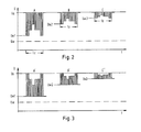
- FIG. 2 shows how the circuit shown in FIG. 1 works in a negative representation, for which the changeover switch 28 is in the N position.
- Three different signal curves are shown over time, which occur at the output of the second amplifier stage 12 and are thus input signals for driving the picture tube 10.
- the signal profiles should each correspond to an image line to be displayed on the picture tube 10 and therefore occur within a picture line time tz. They differ in the amplification set at amplifier stage 11, however, they have the same information content.
- the modulation takes place in the first signal curve between a black potential Us and a white potential Uw1, in the second signal curve between the black potential Us and a white potential Uw2 and in the third signal curve C between the black potential Us and a white potential Uw3.
- Each modulation lies between the black potential Us and a white potential Uw, which corresponds to the white value.
- the white potentials Uw1, Uw2 and Uw3 are gray potentials.
- the reference potential which is supplied to the comparator 25 for the positive display via the changeover switch 28, were only output by a differently dimensioned voltage divider, it would be dimensioned for all signal profiles A ', B' and C 'in such a way that the constant white value Uw is decisive would.
- the signal profiles A ', B' and C 'shown in FIG. 3 would then have matching white values Uw and would not reach the black value Us. The adjustment of the contrast and / or the brightness then required when switching from negative to positive display is thus avoided by the invention.
Landscapes
- Engineering & Computer Science (AREA)
- Computer Hardware Design (AREA)
- Signal Processing (AREA)
- Radar, Positioning & Navigation (AREA)
- Remote Sensing (AREA)
- Physics & Mathematics (AREA)
- Multimedia (AREA)
- General Physics & Mathematics (AREA)
- Theoretical Computer Science (AREA)
- Television Receiver Circuits (AREA)
- Controls And Circuits For Display Device (AREA)
- Liquid Crystal Display Device Control (AREA)
- Transforming Electric Information Into Light Information (AREA)
Applications Claiming Priority (2)
| Application Number | Priority Date | Filing Date | Title |
|---|---|---|---|
| DE4008946 | 1990-03-20 | ||
| DE19904008946 DE4008946C1 (en) | 1990-03-20 | 1990-03-20 | Control circuit for monochrome picture tube - changes positive polarity reference potential with amplification of picture signal amplifier |
Publications (2)
| Publication Number | Publication Date |
|---|---|
| EP0448086A2 true EP0448086A2 (fr) | 1991-09-25 |
| EP0448086A3 EP0448086A3 (en) | 1992-03-04 |
Family
ID=6402652
Family Applications (1)
| Application Number | Title | Priority Date | Filing Date |
|---|---|---|---|
| EP19910104363 Ceased EP0448086A3 (en) | 1990-03-20 | 1991-03-20 | Control circuit for a monochrome picture tube |
Country Status (2)
| Country | Link |
|---|---|
| EP (1) | EP0448086A3 (fr) |
| DE (1) | DE4008946C1 (fr) |
Families Citing this family (1)
| Publication number | Priority date | Publication date | Assignee | Title |
|---|---|---|---|---|
| JPH11205709A (ja) * | 1998-01-08 | 1999-07-30 | Sony Corp | 表示装置 |
Family Cites Families (3)
| Publication number | Priority date | Publication date | Assignee | Title |
|---|---|---|---|---|
| US3249694A (en) * | 1962-08-09 | 1966-05-03 | Hazeltine Research Inc | Black level stabilization system for a television receiver |
| US4679087A (en) * | 1984-03-12 | 1987-07-07 | Loge/Dunn Instruments, Inc. | Method and apparatus for photographing video images of either polarity without CRT brightness or contrast readjustment |
| EP0392100A1 (fr) * | 1989-04-13 | 1990-10-17 | International Business Machines Corporation | Appareil de visualisation à tube à rayons cathodiques avec contrôle d'intensité modifié |
-
1990
- 1990-03-20 DE DE19904008946 patent/DE4008946C1/de not_active Expired - Lifetime
-
1991
- 1991-03-20 EP EP19910104363 patent/EP0448086A3/de not_active Ceased
Also Published As
| Publication number | Publication date |
|---|---|
| EP0448086A3 (en) | 1992-03-04 |
| DE4008946C1 (en) | 1991-06-20 |
Similar Documents
| Publication | Publication Date | Title |
|---|---|---|
| DE69414081T2 (de) | Verstärker mit Offsetgleichspannungskorrektur | |
| DE2845816C2 (de) | Schaltung zur Kontrasterhöhung eines Videosignales | |
| DE2252181C3 (de) | Videoverstärker für ein Farbfernsehbildüberwachungsgerät | |
| DE69125433T2 (de) | Videosignalverarbeitungsschaltung | |
| DE19922540A1 (de) | Bildanzeigevorrichtung | |
| DE864887C (de) | Selbsttaetige Verstaerkungsregelung | |
| DE2819774C3 (de) | Helligkeitsregler für einen Übertragungskanal zur Verarbeitung eines Videosignals | |
| DE3632486C2 (fr) | ||
| DE3744110C2 (fr) | ||
| EP0448086A2 (fr) | Circuit de commande d'un tube image monochrome | |
| DE69431138T2 (de) | Nichtlineare Videosignalverarbeitung | |
| DE4316526B4 (de) | Sender mit einem steuerbaren Leistungsverstärker | |
| EP0750807A1 (fr) | Amplificateur | |
| DE68921427T2 (de) | Vorrichtung zur Wiederherstellung des Gleichstroms. | |
| DE1276134B (de) | Wobbelsender mit elektronischer Frequenzsteuerung | |
| DE69734375T2 (de) | Bildanzeigevorrichtung mit Bus-gesteuerter Kompensationsschaltung unter Verwendung eines Pulsbreitenmodulationssignales # | |
| DE2749767B2 (de) | Schaltungsanordnung zur Helligkeitssteuerung von Leuchtdioden in Leuchtdiodenfeldern | |
| DE4315092C2 (de) | Anzeigemonitor | |
| DE2018923A1 (de) | Schnelle Stromschaltverstärker (Ablenkvers tSrker) | |
| EP0793159B1 (fr) | Circuit pour générer une tension d'alimentation | |
| DE69322699T2 (de) | Weckschaltung für einen Telefonapparat | |
| DE3242127C2 (fr) | ||
| DE2611274C3 (de) | Regelverstärkerschaltung mit Symmetrierwirkung | |
| DE69522623T2 (de) | Steuerschaltung zum Einstellen einer Sperrspannung und einer Ansteuerspannung, z.B. für Kathodenstrahlröhren, und diese Schaltung enthaltende Videoausrüstung | |
| DE1942871A1 (de) | Automatische Synchronisierungsvorrichtung |
Legal Events
| Date | Code | Title | Description |
|---|---|---|---|
| PUAI | Public reference made under article 153(3) epc to a published international application that has entered the european phase |
Free format text: ORIGINAL CODE: 0009012 |
|
| AK | Designated contracting states |
Kind code of ref document: A2 Designated state(s): AT BE CH DE DK ES FR GB GR IT LI LU NL SE |
|
| RBV | Designated contracting states (corrected) |
Designated state(s): FR GB IT NL SE |
|
| PUAL | Search report despatched |
Free format text: ORIGINAL CODE: 0009013 |
|
| REG | Reference to a national code |
Ref country code: DE Ref legal event code: 8566 |
|
| AK | Designated contracting states |
Kind code of ref document: A3 Designated state(s): AT BE CH DE DK ES FR GB GR IT LI LU NL SE |
|
| 17P | Request for examination filed |
Effective date: 19920205 |
|
| 17Q | First examination report despatched |
Effective date: 19931123 |
|
| STAA | Information on the status of an ep patent application or granted ep patent |
Free format text: STATUS: THE APPLICATION HAS BEEN REFUSED |
|
| 18R | Application refused |
Effective date: 19940515 |