EP0445780B1 - Système d'enregistrement et de reproduction de signal d'image - Google Patents
Système d'enregistrement et de reproduction de signal d'image Download PDFInfo
- Publication number
- EP0445780B1 EP0445780B1 EP91103424A EP91103424A EP0445780B1 EP 0445780 B1 EP0445780 B1 EP 0445780B1 EP 91103424 A EP91103424 A EP 91103424A EP 91103424 A EP91103424 A EP 91103424A EP 0445780 B1 EP0445780 B1 EP 0445780B1
- Authority
- EP
- European Patent Office
- Prior art keywords
- signal
- reproducing
- sampling
- reproduced
- image signal
- Prior art date
- Legal status (The legal status is an assumption and is not a legal conclusion. Google has not performed a legal analysis and makes no representation as to the accuracy of the status listed.)
- Expired - Lifetime
Links
Images


Classifications
-
- H—ELECTRICITY
- H04—ELECTRIC COMMUNICATION TECHNIQUE
- H04N—PICTORIAL COMMUNICATION, e.g. TELEVISION
- H04N9/00—Details of colour television systems
- H04N9/79—Processing of colour television signals in connection with recording
- H04N9/793—Processing of colour television signals in connection with recording for controlling the level of the chrominance signal, e.g. by means of automatic chroma control circuits
-
- H—ELECTRICITY
- H04—ELECTRIC COMMUNICATION TECHNIQUE
- H04N—PICTORIAL COMMUNICATION, e.g. TELEVISION
- H04N9/00—Details of colour television systems
- H04N9/79—Processing of colour television signals in connection with recording
- H04N9/797—Processing of colour television signals in connection with recording for recording the signal in a plurality of channels, the bandwidth of each channel being less than the bandwidth of the signal
- H04N9/7973—Processing of colour television signals in connection with recording for recording the signal in a plurality of channels, the bandwidth of each channel being less than the bandwidth of the signal by dividing the luminance or colour component signal samples or frequency bands among a plurality of recording channels
-
- H—ELECTRICITY
- H04—ELECTRIC COMMUNICATION TECHNIQUE
- H04N—PICTORIAL COMMUNICATION, e.g. TELEVISION
- H04N9/00—Details of colour television systems
- H04N9/79—Processing of colour television signals in connection with recording
- H04N9/87—Regeneration of colour television signals
Definitions
- This invention relates to an image signal recording and reproducing system for recording an image signal on a recording medium and for reproducing the image signal recorded on the recording medium.
- a still video system (hereinafter referred to as the SV system) has been known as an apparatus for recording and reproducing a still image signal.
- the SV system is arranged to frequency-modulate the current TV signal of, for example, the NTSC system and to record the frequency-modulated TV signal on a magnetic disc called a video floppy disc. Therefore, the image signal recorded and reproduced by the SV system has been arranged to have a degree of resolution which approximately conforms to the current TV system.
- the HDTV system has about 1000 scanning lines which are about twice as many as those of the current NTSC system and also has a horizontal signal band matching with those many scanning lines.
- CHSV compatible high-definition still video
- a luminance signal which has been offset-sampled at intervals of time Ts as shown in Fig. 1 of the accompanying drawings is first divided into four field image planes Ai, Bi, Ci and Di (i: 1, 2, ---) and recorded in four tracks on a video floppy disc in accordance with the current SV format.
- the reproduced signal is re-sampled to restore the offset-sampled luminance signal.
- the signal thus restored is stored in a frame memory.
- a picture element interpolation process is carried out with picture elements stored in the frame memory.
- the above-stated CHSV system performs "analog transmission of sampled values" in a manner as shown in Fig. 2 through a transmission path consisting of frequency-modulating, frequency-demodulating and electro-magnetic converting elements and by performing re-sampling at the time of reproduction.
- a series of sample values to be supplied to the transmission path is not in an impulse state as shown in Fig. 2 but has a finite width as shown in Fig. 3. Since the transmission path has a low-pass filter characteristic (Nyquist characteristics), it is necessary, for accurate restoration of the signal, to make aperture correction for the signal after it has passed through the transmission path as shown in Fig. 3.
- the transmission path has a low-pass filter characteristic and (ii) that the re-sampling process is correctly performed on the signal receiving side.
- a phase reference signal which serves as a reference to the phase of re-sampling is added to the image signal to be transmitted. Then, on the signal receiving side, the phase of re-sampling can be controlled in accordance with the phase reference signal included in the image signal transmitted.
- Fig. 4 is a block diagram showing in outline the arrangement of an image signal reproducing apparatus conforming to the CHSV system. To simplify the description, Fig. 4 includes only luminance signal reproducing blocks.
- a signal recorded on a video floppy disc 501 is reproduced by a reproducing head 502.
- the reproduced signal is supplied to a reproduction processing circuit 503.
- the reproduction processing circuit 503 then performs frequency demodulation and deemphasis processes, etc. on the signal and outputs a reproduced image signal.
- the reproduced image signal is subjected to an aperture correction process which is performed by an aperture correction filter 505, to a clamping process which is performed by a clamp circuit 506 and is then supplied to an analog-to-digital (A/D) converter 507.
- an aperture correction process which is performed by an aperture correction filter 505
- a clamping process which is performed by a clamp circuit 506 and is then supplied to an analog-to-digital (A/D) converter 507.
- a re-sampling clock signal generating circuit 504 separates, from the signal reproduced by the reproducing head 502, only a time base correcting pilot signal component which has been frequency-multiplexed with the image signal at the time of recording.
- a PLL (phase-locked loop) circuit disposed within the re-sampling clock signal generating circuit 504 then forms, on the basis of the pilot signal, a re-sampling clock signal fs which follows time base variations taking place in the reproduced image signal.
- the re-sampling clock signal fs which is thus output from the re-sampling clock signal generating circuit 504 is supplied to a variable delay circuit 508.
- the variable delay circuit 508 controls the phase of the re-sampling clock signal and supplies it to the A/D converter 507.
- the phase controlling action of the variable delay circuit 508 on the re-sampling clock signal fs is performed under the control of a phase control signal generating circuit 509.
- the phase control signal generating circuit 509 is arranged to receive a re-sampled image signal from the A/D converter 507 and to form a phase control signal PC from the re-sampled image signal according to a sample value corresponding to the phase reference signal part thereof.
- the phase control signal PC thus formed is supplied to the variable delay circuit 508 to adjust the phase of the re-sampling clock signal to a correct phase.
- the re-sampling clock signal which is thus adjusted to have a correct phase is supplied to the A/D converter 507 to be used for digitizing the reproduced image signal.
- the digital reproduced image signal thus obtained is Nyquist-equalized by an automatic equalizer 510.
- the automatic equalizer 510 is formed by a digital filter.
- the equalizing characteristic of the automatic equalizer 510 is arranged to be adjustable by varying the tap coefficient of the digital filter.
- the tap coefficient of the digital filter is arranged to be variable by means of a coefficient control circuit 511.
- the tap coefficient varying action is performed as follows:
- a subtracter 512 is arranged to receive the re-sampled image signal output from the automatic equaliger 510 and an ideal response waveform signal In generated by an oscillator which is not shown.
- the subtracter 512 produces a difference between the ideal response waveform signal In and the re-sample value of the phase reference signal part of the re-sampled image signal as a result of subtraction.
- the coefficient control circuit 511 forms and produces a tap coefficient selection signal for changing the tap coefficient of the digital filter included in the automatic equalizer 510.
- the automatic equalizer 510 selects a tap coefficient most apposite to the digital filter.
- the re-sampled image signal is thus automatically Nyquist-equalized.
- the digital reproduced image signal which has been thus equalized is stored in an image memory 513.
- the above-stated reproduced signal processing action is performed on the signal reproduced from each of the four tracks of the video floppy disc 501.
- a series of sample values which is shown in Fig. 2 and which corresponds to the offset sampled luminance signal shown in Fig. 1 is eventually stored in the image memory 513.
- An interpolation circuit 514 then performs an interpolation process by using the sample data stored in the image memory 513. After the interpolation process, the sample data is read out from the image memory 513. The data read out is converted into an analog signal by a digital-to-analog (D/A) converter 515. The analog signal thus obtained is output through an LPF (low-pass filter) 516 as a reproduced image signal.
- D/A digital-to-analog
- phase reference signal to be added to the image signal either an impulse type signal or a step type signal is employed. Further, to let the phase reference signal have an advantage over a noise or the like which might mix therewith, the phase reference signal is generally added at about a 100% level relative to the white level of the image signal.
- Fig. 5 shows the waveform of the phase reference signal reproduced by the reproducing operation in a case where the impulse type phase reference signal is added to the image signal in recording. If the step type phase reference signal is added to the image signal in recording, the waveform of the reproduced phase reference signal becomes as shown in Fig. 6.
- a signal of the type having a sudden level change brings about a ringing component which is a transient vibration. Such a ringing component occurs not only in the phase reference signal part but also in other parts where the level of the image signal suddenly changes.
- the dynamic range of the A/D converter 507 must be set at a value larger than the above-stated value.
- the dynamic range of the A/D converter being thus broadened, it would increase a quantization noise if the number of quantization bits remains the same.
- the dynamic range of the A/D converter is set at a value which is about 1.4 X A (A: the dynamic range of the input signal of the A/D converter)
- the quantization noise would increase by about 3 dB. The noise deteriorates the quality of the reproduced picture. This presents such a problem that the quantization bits are wasted.
- the document by Nagaoka et al: 'A two-channel recording VCR using orthogonal arrangement of heads' published in IEEE Transactions on Consumer Electronics vol. 35, no. 3, August 1989, NEW YORK, pages 202 - 206 describes a level and gain compensation circuit for a two-channel video tape recorder.
- the circuit comprises a comparator for comparing the resampled signal to a threshold and an AGC amplifier for adjusting the amplitude of the reproduced signal whereby the gain of the AGC amplifier is controlled by the comparison result.
- Fig. 1 shows luminance signal sampling points obtained by the CHSV system.
- Figs. 2 and 3 show the analog transmission of sample values.
- Fig. 4 is a block diagram showing in outline the arrangement of an image signal reproducing apparatus arranged according to the CHSV system.
- Fig. 5 shows the waveform of a reproduced phase reference signal obtained at the time of reproduction in a case where an impulse type phase reference signal is added to an image signal in recording.
- Fig. 6 shows the waveform of a reproduced phase reference signal obtained at the time of reproduction in a case where a step type phase reference signal is added to an image signal in recording.
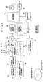
- Fig. 7 is a block diagram showing in outline the arrangement of an image signal reproducing apparatus which conforms to the CHSV system and is arranged according to this invention as a first embodiment thereof.
- Figs. 8(a) and 8(b) show how a quantization range varies in relation to the input signal of an A/D converter according to the correctness or incorrectness of the phase of a re-sampling action performed on a digital reproduced image signal output from the A/D converter.
- Fig. 9 is a block diagram showing in outline the arrangement of an image signal reproducing apparatus which conforms to the CHSV system and is arranged as a second embodiment of the invention.
- Fig. 7 is a block diagram showing in outline the arrangement of an image signal reproducing apparatus which conforms to the CHSV system and is arranged according to this invention as a first embodiment thereof.
- the same components as those of the apparatus shown in Fig. 4 are indicated by the same reference numerals and symbols, and the details of them are omitted from description.
- a reproduced image signal which has undergone the aperture correction process at the aperture correction filter 505 is supplied via a variable-gain amplifier 101 and a clamp circuit 102 to the A/D converter 507.
- the A/D converter 507 then performs a re-sampling action on the reproduced image signal to produce a digital reproduced image signal.
- a phase control signal generating circuit 103 is arranged to form a phase control signal PC according to the sample value of a phase reference signal part which is included in the digital reproduced image signal output from the A/D converter 507.
- the phase control signal PC is supplied to the variable delay circuit 508.
- phase control signal generating circuit 103 detects the re-sampling phase of the digital reproduced image signal output from the A/D converter 507 to find if it is correctly controlled.
- the circuit 103 produces an indication signal P at "0" if the re-sampling phase of the digital reproduced image signal is found to be incorrect and at "1" if the re-sampling phase is found to be correct.
- the above-stated variable-gain amplifier 101 is arranged to change the gain of the reproduced image signal from one value over to another in accordance with a gain control signal VG1 or VG2 which is selected by a switch S1.
- the clamp circuit 102 is arranged to change a clamp potential from one value over to another in accordance with a clamp potential control signal VR1 or VR2 which is selected by a switch S2.
- the switching actions of these switches S1 and S2 are performed according to the above-stated indication signal P in the following manner:
- the switch S1 selects the gain control signal VG1 and the switch S2 the clamp potential control signal VR1 when the indication signal P indicates "0".
- the switch S1 selects the gain control signal VR2 and the Switch S2 the clamp potential control signal VR2 when the indication signal P indicates "1".
- the quantization range of the A/D converter 507 in relation to the input signal is changed as shown in Fig. 8(a) when the indication signal P is at "0" and as shown in Fig. 8(b) when the indication signal P is at "1".
- the quantization range of the A/D converter 507 shown in Fig. 8(b) becomes narrower than that shown in Fig. 8(a) by a minute amount 2 ⁇ .
- the range of the quantizing action of the A/D converter 507 on its input signal is arranged to be changed by varying both the gain control signal VG which controls the gain of the variable-gain amplifier 101 and the clamp potential control signal VR which controls the clamp potential of the clamp circuit 102.
- this arrangement may be changed to vary the quantization range of the A/D converter 507 by varying only one of the gain control signal VG and the clamp potential control signal VR.
- the arrangement of the apparatus can be simplified by this.
- the invention is applied to the image signal reproducing apparatus which is in conformity to the CHSV system.
- the invention is not limited to the CHSV system but is applicable also to other systems using the analog transmission of sample values, such as the MUSE system or the like.
- the embodiment is arranged to change the quantization range of the A/D converter according to the correctness or incorrectness of the phase of the re-sampling action on the digital reproduced image signal output from the A/D converter.
- the dynamic range of the input signal of the A/D converter is changed to minimize the quantization range of the input signal of the A/D converter.
- Fig. 9 is a block diagram showing in outline the arrangement of an image signal reproducing apparatus which conforms to the CHSV system and is arranged also according to this invention as a second embodiment thereof.
- the same components as those of the apparatus shown in Fig. 4 are indicated by the same reference numerals, and the details of them are omitted from description.
- a reproduced image signal which has been subjected to the aperture correction process of the aperture correction filter 505 is supplied via a variable-gain amplifier 201 and a clamp circuit 202 to the A/D converter 507.
- the reproduced image signal is re-sampled and converted into a digital reproduced image signal by the A/D converter 507.
- the digital reproduced image signal is supplied from the A/D converter 507 to the automatic equalizer 510, a phase control signal generating circuit 203 and a maximum-value/minimum-value detecting circuit 517.
- the phase control signal generating circuit 203 forms a phase control signal PC according to a sample value corresponding to a phase reference signal part included in the digital reproduced image signal output from the A/D converter 507.
- the phase control signal PC is supplied to the variable delay circuit 508.
- the maximum-value/minimum-value detecting circuit 517 is arranged to detect the maximum and minimum values of the digital reproduced image signal supplied to the circuit 517 during a given period of time.
- the period of time during which the maximum and minimum values of the digital reproduced image signal are detected by the maximum-value/minimum-value detecting circuit 517 is controlled by a reset pulse supplied from the outside. Further, a reset signal having the same frequency as the frequency of vertical synchronizing pulses may be used for the above-stated reset pulse.
- the maximum and minimum values detected by the maximum-value/minimum-value detecting circuit 517 are supplied to a dynamic range setting circuit 518 as maximum value data "max” and minimum value data "min” respectively.
- the dynamic range setting circuit 518 is arranged to form, from the maximum value data "max” and the minimum value data "min", a clamp potential control signal VR for controlling the clamp potential of the clamp circuit 202 and a gain control signal GR for controlling the gain of the variable-gain amplifier 201.
- the gain of the variable-gain amplifier 201 and the clamp potential of the clamp circuit 202 are controlled in such a way as to have the maximum and minimum levels of quantization close to the maximum and minimum values of the digital reproduced image signal output from the A/D converter 507 respectively.
- the dynamic range of the signal supplied to the A/D converter 507 is controlled to be within a range from "A" to "A + 2B" as shown in Fig. 6, so that the quantization bits can be prevented from being wasted.
- the quantization range of the A/D converter 507 relative to its input signal is arranged to be varied by controlling both the gain of the variable-gain amplifier 201 and the clamp potential of the clamp circuit 202 according to the maximum and minimum values of the digital reproduced image signal output from the A/D converter 507 during a given period of time.
- this arrangement may be changed to vary the quantization range for the input signal of the A/D converter 507 by controlling only one of the gain of the variable-gain amplifier 201 and the clamp potential of the clamp circuit 202.
- the arrangement of the embodiment can be simplified by this modification.
- this embodiment is arranged to automatically adjust the input signal quantization range of the A/D converter in such a way as to be always apposite to the digital reproduced image signal output from the A/D converter. Therefore, the quantization bits of the A/D converter can be prevented from being wasted.
- an image signal recording and reproducing system can be arranged in a simple manner to be capable of recording an image signal on a recording medium and reproducing the recorded image signal without deteriorating the signal.
- An image signal recording and reproducing system for recording an image signal on a recording medium and for reproducing the image signal recorded on the recording medium is arranged to perform a reproducing action on the recording medium on which a sampled image signal formed by sampling the image signal is recorded; to sample a reproduced signal reproduced from the recording medium; and, in outputting a sampled reproduced signal, the level of the reproduced signal to be sampled is controlled according to the sampling phase of the reproduced signal.
Landscapes
- Engineering & Computer Science (AREA)
- Multimedia (AREA)
- Signal Processing (AREA)
- Television Signal Processing For Recording (AREA)
- Picture Signal Circuits (AREA)
Claims (9)
- Système d'enregistrement et de reproduction de signal d'image destiné à enregistrer un signal d'image sur un support d'enregistrement (501) et à reproduire le signal d'image enregistré sur le support d'enregistrement (501), comprenant :(a) un moyen de reproduction (502, 503, 505) destiné à reproduire un signal à partir du support d'enregistrement (501) sur lequel un signal d'image est enregistré et à sortir le signal reproduit à partir du support d'enregistrement (501),(b) un moyen de génération de signal d'horloge d'échantillonnage (504, 508) destiné à générer un signal d'horloge d'échantillonnage qui est verrouillé en phase sur la sortie du signal reproduit provenant dudit moyen de reproduction (502, 503, 505),(c) un moyen d'échantillonnage (507) destiné à échantillonner le signal reproduit qui sort dudit moyen de reproduction (502, 503, 505) conformément au signal d'horloge d'échantillonnage qui sort dudit moyen de génération de signal d'horloge d'échantillonnage (504, 508), et à sortir un signal échantillonné, et(d) un moyen de commande de niveau (101, 102, 103) destiné à commander le niveau du signal reproduit fourni à partir dudit moyen de reproduction (502, 503, 505) audit moyen d'échantillonnage (507) conformément à un état de la phase d'échantillonnage dudit moyen d'échantillonnage (507).
- Système selon la revendication 1, dans lequel ledit moyen d'échantillonnage (507) comprend un convertisseur analogique vers numérique agencé pour convertir le signal reproduit qui sort dudit moyen de reproduction (502, 503, 505) en un signal numérique.
- Système selon la revendication 1 ou 2, dans lequel ledit moyen de commande de niveau (101, 102, 103) comprend :(a) un moyen d'amplification (101) destiné à amplifier le signal reproduit qui sort dudit moyen de reproduction (502, 503, 505) et à sortir le signal amplifié, et/ou(b) un moyen de rétablissement de niveau (102) destiné à rétablir le niveau du signal reproduit amplifié par ledit moyen d'amplification et à sortir le signal à niveau rétabli, et(c) un moyen de commande (103) destiné à commander la caractéristique d'amplification dudit moyen d'amplification (101) et/ou la caractéristique de rétablissement de niveau dudit moyen de rétablissement de niveau (102) conformément au niveau du signal échantillonné qui sort dudit moyen d'échantillonnage (507).
- Système d'enregistrement et de reproduction du signal d'image destiné à enregistrer un signal d'image sur un support d'enregistrement (501) et à reproduire le signal d'image enregistré sur le support d'enregistrement (501), comprenant :(a) un moyen de reproduction (502, 503, 505) destiné à reproduire un signal à partir du support d'enregistrement (501) sur lequel un signal d'image est enregistré et à sortir le signal reproduit à partir du support d'enregistrement (501),(b) un moyen d'échantillonnage (504, 507) destiné à échantillonner le signal reproduit qui sort dudit moyen de reproduction (502, 503, 505) et à sortir le signal échantillonné,(c) un moyen de rétablissement de niveau (202) destiné à rétablir le niveau du signal reproduit qui sort dudit moyen de reproduction (502, 503, 505) et à sortir le signal à niveau rétabli, et(d) un moyen de commande (517, 518) destiné à commander les caractéristiques de rétablissement de niveau dudit moyen de rétablissement de niveau (202) conformément au niveau du signal échantillonné qui sort dudit moyen d'échantillonnage (504, 507).
- Système selon la revendication 4, dans lequel ledit moyen d'échantillonnage (504, 507) comprend un moyen de génération de signal d'horloge d'échantillonnage (504) destiné à générer un signal d'horloge d'échantillonnage qui est verrouillé en phase sur le signal reproduit qui sort dudit moyen de reproduction (502, 503, 505), et le signal reproduit qui sort dudit moyen de reproduction (502, 503, 505) est agencé pour être échantillonné conformément au signal d'horloge d'échantillonnage qui sort dudit moyen de génération de signal d'horloge d'échantillonnage (504) et pour être sorti en tant que signal échantillonné.
- Système selon la revendication 4 ou 5, dans lequel ledit moyen d'échantillonnage (504, 507) comprend un convertisseur analogique vers numérique (507) agencé pour convertir le signal reproduit qui sort dudit moyen de reproduction (502, 503, 505) en un signal numérique.
- Système selon l'une quelconque des revendications précédentes 4 à 6, dans lequel ledit système d'enregistrement et de reproduction de signal d'image comprend en outre un moyen d'amplification (201) destiné à amplifier le signal reproduit qui sort dudit moyen de reproduction (502, 503, 505) et à sortir le signal amplifié.
- Système selon la revendication 7, dans lequel ledit moyen de rétablissement de niveau (202) est agencé pour rétablir le niveau du signal reproduit amplifié par ledit moyen d'amplification (201) et pour sortir le signal à niveau rétabli, et ledit moyen de commande (517, 518) est agencé pour commander la caractéristique d'amplification dudit moyen d'amplification (201).
- Système selon l'une quelconque des revendications précédentes 4 à 8, dans lequel ledit système d'enregistrement et de reproduction de signal d'image comprend en outre un moyen de détection (517) destiné à détecter la plage dynamique ou les valeurs minimum et maximum du signal échantillonné qui sort pendant un intervalle de temps prédéterminé dudit moyen d'échantillonnage (504), 507) et ledit moyen de commande (517, 518) est agencé pour exécuter son opération de commande conformément au résultat de la détection faite par ledit moyen de détection (517).
Applications Claiming Priority (4)
| Application Number | Priority Date | Filing Date | Title |
|---|---|---|---|
| JP53516/90 | 1990-03-07 | ||
| JP2053516A JP2928887B2 (ja) | 1990-03-07 | 1990-03-07 | 画像信号処理装置 |
| JP53515/90 | 1990-03-07 | ||
| JP2053515A JP2928886B2 (ja) | 1990-03-07 | 1990-03-07 | 画像信号処理装置 |
Publications (3)
| Publication Number | Publication Date |
|---|---|
| EP0445780A2 EP0445780A2 (fr) | 1991-09-11 |
| EP0445780A3 EP0445780A3 (en) | 1993-06-09 |
| EP0445780B1 true EP0445780B1 (fr) | 1997-07-09 |
Family
ID=26394220
Family Applications (1)
| Application Number | Title | Priority Date | Filing Date |
|---|---|---|---|
| EP91103424A Expired - Lifetime EP0445780B1 (fr) | 1990-03-07 | 1991-03-06 | Système d'enregistrement et de reproduction de signal d'image |
Country Status (3)
| Country | Link |
|---|---|
| US (1) | US5438558A (fr) |
| EP (1) | EP0445780B1 (fr) |
| DE (1) | DE69126718T2 (fr) |
Families Citing this family (3)
| Publication number | Priority date | Publication date | Assignee | Title |
|---|---|---|---|---|
| US5424881A (en) | 1993-02-01 | 1995-06-13 | Cirrus Logic, Inc. | Synchronous read channel |
| JPH08212736A (ja) * | 1995-02-02 | 1996-08-20 | Toshiba Corp | 磁気ディスク装置におけるサーボ信号検出装置及びサーボ信号検出方法 |
| US20100166257A1 (en) * | 2008-12-30 | 2010-07-01 | Ati Technologies Ulc | Method and apparatus for detecting semi-transparencies in video |
Family Cites Families (15)
| Publication number | Priority date | Publication date | Assignee | Title |
|---|---|---|---|---|
| JPS5327010A (en) * | 1976-08-25 | 1978-03-13 | Sony Corp | Signal tran smitter |
| US4169219A (en) * | 1977-03-30 | 1979-09-25 | Beard Terry D | Compander noise reduction method and apparatus |
| JPS5948447B2 (ja) * | 1977-07-20 | 1984-11-27 | ソニー株式会社 | 信号再生装置の利得補償回路 |
| US4575749A (en) * | 1983-07-28 | 1986-03-11 | Rca Corporation | Component companding in a multiplexed component system |
| US4742392A (en) * | 1983-08-04 | 1988-05-03 | Canon Kabushiki Kaisha | Clamp circuit with feed back |
| JPS6337815A (ja) * | 1986-07-30 | 1988-02-18 | Toshiba Corp | 記録デ−タ再生装置 |
| JPH07105936B2 (ja) * | 1987-03-16 | 1995-11-13 | パイオニア株式会社 | 読取信号の時間軸制御装置 |
| JP2690933B2 (ja) * | 1988-04-06 | 1997-12-17 | 株式会社日立製作所 | 信号判別装置 |
| US4891716A (en) * | 1988-10-03 | 1990-01-02 | Datatape Incorporated | Autocalibration of a data signal channel through simultaneous control signals |
| JPH02185182A (ja) * | 1989-01-12 | 1990-07-19 | Canon Inc | 画像信号再生装置 |
| AU629300B2 (en) * | 1989-02-28 | 1992-10-01 | Sony Corporation | Digital signal reproducing apparatus |
| JP2667522B2 (ja) * | 1989-07-06 | 1997-10-27 | 株式会社日立製作所 | 光ディスク装置 |
| US5077623A (en) * | 1990-03-30 | 1991-12-31 | Ampex Corporation | Method and apparatus for automatically optimizing the record current in a tape recorder using a reference tape |
| US5220466A (en) * | 1991-05-21 | 1993-06-15 | International Business Machines Corporation | Method and apparatus for digital filter control in a partial-response maximum-likelihood disk drive system |
| US5233482A (en) * | 1991-07-31 | 1993-08-03 | International Business Machines Corporation | Thermal asperity compensation for PRML data detection |
-
1991
- 1991-03-06 EP EP91103424A patent/EP0445780B1/fr not_active Expired - Lifetime
- 1991-03-06 DE DE69126718T patent/DE69126718T2/de not_active Expired - Fee Related
-
1993
- 1993-11-10 US US08/150,588 patent/US5438558A/en not_active Expired - Lifetime
Also Published As
| Publication number | Publication date |
|---|---|
| EP0445780A3 (en) | 1993-06-09 |
| EP0445780A2 (fr) | 1991-09-11 |
| DE69126718D1 (de) | 1997-08-14 |
| US5438558A (en) | 1995-08-01 |
| DE69126718T2 (de) | 1998-01-15 |
Similar Documents
| Publication | Publication Date | Title |
|---|---|---|
| US4805040A (en) | Drop-out correction circuit in an apparatus for correcting time base error with inhibition of time-base information during dropout | |
| EP0542540B1 (fr) | Circuit égaliseur de reproduction pour un dispositif de reproduction magnétique numérique | |
| US5270876A (en) | Apparatus for reproducing data recorded on a magnetic recording medium | |
| EP0445780B1 (fr) | Système d'enregistrement et de reproduction de signal d'image | |
| US5296929A (en) | Automatic correction apparatus for video signal of digital VTR | |
| US5212562A (en) | Image signal reproducing apparatus having memory function | |
| EP0414556B1 (fr) | Circuit de compensation pour compenser les distorsions d'un signal vidéo en détectant les distorsions d'un signal en rampe dans le signal vidéo | |
| US5663844A (en) | Signal reproducing apparatus having waveform equalizing function | |
| KR100316675B1 (ko) | 클록신호생성장치 | |
| US5347316A (en) | Image information transmission system having time base variation correcting function | |
| JP2928887B2 (ja) | 画像信号処理装置 | |
| JP2928886B2 (ja) | 画像信号処理装置 | |
| JP2532416B2 (ja) | リンギング軽減装置 | |
| JPH0681293B2 (ja) | 再生装置 | |
| JPS63113982A (ja) | デジタル信号検出回路 | |
| US5481368A (en) | Frequency demodulating apparatus with inversion compensation | |
| JP2801291B2 (ja) | 情報信号再生装置 | |
| JPH08190765A (ja) | 記録装置及び再生装置 | |
| JPH07264540A (ja) | 磁気記録再生装置 | |
| JPH0417512B2 (fr) | ||
| JPS63113981A (ja) | デジタル信号検出回路 | |
| JPS58215711A (ja) | デイジタル信号の再生処理装置 | |
| JPH04183081A (ja) | 画像再生装置 | |
| JPH0677370B2 (ja) | デイジタル記録再生装置における自動等化方法及び装置 | |
| JPS60258761A (ja) | デジタル磁気記録におけるパルス再生回路 |
Legal Events
| Date | Code | Title | Description |
|---|---|---|---|
| PUAI | Public reference made under article 153(3) epc to a published international application that has entered the european phase |
Free format text: ORIGINAL CODE: 0009012 |
|
| AK | Designated contracting states |
Kind code of ref document: A2 Designated state(s): DE FR GB |
|
| PUAL | Search report despatched |
Free format text: ORIGINAL CODE: 0009013 |
|
| AK | Designated contracting states |
Kind code of ref document: A3 Designated state(s): DE FR GB |
|
| 17P | Request for examination filed |
Effective date: 19931026 |
|
| 17Q | First examination report despatched |
Effective date: 19951018 |
|
| GRAG | Despatch of communication of intention to grant |
Free format text: ORIGINAL CODE: EPIDOS AGRA |
|
| GRAH | Despatch of communication of intention to grant a patent |
Free format text: ORIGINAL CODE: EPIDOS IGRA |
|
| GRAH | Despatch of communication of intention to grant a patent |
Free format text: ORIGINAL CODE: EPIDOS IGRA |
|
| GRAH | Despatch of communication of intention to grant a patent |
Free format text: ORIGINAL CODE: EPIDOS IGRA |
|
| GRAA | (expected) grant |
Free format text: ORIGINAL CODE: 0009210 |
|
| AK | Designated contracting states |
Kind code of ref document: B1 Designated state(s): DE FR GB |
|
| ET | Fr: translation filed | ||
| REF | Corresponds to: |
Ref document number: 69126718 Country of ref document: DE Date of ref document: 19970814 |
|
| PLBE | No opposition filed within time limit |
Free format text: ORIGINAL CODE: 0009261 |
|
| STAA | Information on the status of an ep patent application or granted ep patent |
Free format text: STATUS: NO OPPOSITION FILED WITHIN TIME LIMIT |
|
| 26N | No opposition filed | ||
| REG | Reference to a national code |
Ref country code: GB Ref legal event code: IF02 |
|
| PGFP | Annual fee paid to national office [announced via postgrant information from national office to epo] |
Ref country code: GB Payment date: 20090331 Year of fee payment: 19 |
|
| PGFP | Annual fee paid to national office [announced via postgrant information from national office to epo] |
Ref country code: DE Payment date: 20090331 Year of fee payment: 19 |
|
| PGFP | Annual fee paid to national office [announced via postgrant information from national office to epo] |
Ref country code: FR Payment date: 20090325 Year of fee payment: 19 |
|
| GBPC | Gb: european patent ceased through non-payment of renewal fee |
Effective date: 20100306 |
|
| REG | Reference to a national code |
Ref country code: FR Ref legal event code: ST Effective date: 20101130 |
|
| PG25 | Lapsed in a contracting state [announced via postgrant information from national office to epo] |
Ref country code: FR Free format text: LAPSE BECAUSE OF NON-PAYMENT OF DUE FEES Effective date: 20100331 |
|
| PG25 | Lapsed in a contracting state [announced via postgrant information from national office to epo] |
Ref country code: DE Free format text: LAPSE BECAUSE OF NON-PAYMENT OF DUE FEES Effective date: 20101001 |
|
| PG25 | Lapsed in a contracting state [announced via postgrant information from national office to epo] |
Ref country code: GB Free format text: LAPSE BECAUSE OF NON-PAYMENT OF DUE FEES Effective date: 20100306 |