EP0445323A1 - Dispositif semi-conducteur à effet de champ présentant un trajet de courant formé dans une couche conductrice du substrat semi-conducteur - Google Patents
Dispositif semi-conducteur à effet de champ présentant un trajet de courant formé dans une couche conductrice du substrat semi-conducteur Download PDFInfo
- Publication number
- EP0445323A1 EP0445323A1 EP90104279A EP90104279A EP0445323A1 EP 0445323 A1 EP0445323 A1 EP 0445323A1 EP 90104279 A EP90104279 A EP 90104279A EP 90104279 A EP90104279 A EP 90104279A EP 0445323 A1 EP0445323 A1 EP 0445323A1
- Authority
- EP
- European Patent Office
- Prior art keywords
- conductivity type
- layer
- semiconductor substrate
- field effect
- type
- Prior art date
- Legal status (The legal status is an assumption and is not a legal conclusion. Google has not performed a legal analysis and makes no representation as to the accuracy of the status listed.)
- Withdrawn
Links
- 239000004065 semiconductor Substances 0.000 title claims abstract description 72
- 239000000758 substrate Substances 0.000 title claims abstract description 67
- 230000005669 field effect Effects 0.000 title claims abstract description 26
- 238000009792 diffusion process Methods 0.000 claims description 12
- 238000005530 etching Methods 0.000 abstract description 4
- XUIMIQQOPSSXEZ-UHFFFAOYSA-N Silicon Chemical compound [Si] XUIMIQQOPSSXEZ-UHFFFAOYSA-N 0.000 description 66
- 229910052710 silicon Inorganic materials 0.000 description 66
- 239000010703 silicon Substances 0.000 description 66
- 238000004519 manufacturing process Methods 0.000 description 8
- 238000010438 heat treatment Methods 0.000 description 7
- -1 boron ions Chemical class 0.000 description 6
- 230000015556 catabolic process Effects 0.000 description 6
- 229910052796 boron Inorganic materials 0.000 description 4
- 238000002955 isolation Methods 0.000 description 4
- 230000003647 oxidation Effects 0.000 description 4
- 238000007254 oxidation reaction Methods 0.000 description 4
- 229920002120 photoresistant polymer Polymers 0.000 description 4
- 229910021420 polycrystalline silicon Inorganic materials 0.000 description 4
- 229920005591 polysilicon Polymers 0.000 description 4
- 239000012298 atmosphere Substances 0.000 description 3
- 238000000605 extraction Methods 0.000 description 3
- 239000012535 impurity Substances 0.000 description 3
- 229910000838 Al alloy Inorganic materials 0.000 description 2
- OAICVXFJPJFONN-UHFFFAOYSA-N Phosphorus Chemical compound [P] OAICVXFJPJFONN-UHFFFAOYSA-N 0.000 description 2
- 230000001133 acceleration Effects 0.000 description 2
- XAGFODPZIPBFFR-UHFFFAOYSA-N aluminium Chemical compound [Al] XAGFODPZIPBFFR-UHFFFAOYSA-N 0.000 description 2
- 229910052782 aluminium Inorganic materials 0.000 description 2
- 229910052785 arsenic Inorganic materials 0.000 description 2
- QVGXLLKOCUKJST-UHFFFAOYSA-N atomic oxygen Chemical compound [O] QVGXLLKOCUKJST-UHFFFAOYSA-N 0.000 description 2
- 150000002500 ions Chemical class 0.000 description 2
- 238000000034 method Methods 0.000 description 2
- 239000012299 nitrogen atmosphere Substances 0.000 description 2
- 239000001301 oxygen Substances 0.000 description 2
- 229910052760 oxygen Inorganic materials 0.000 description 2
- 238000002161 passivation Methods 0.000 description 2
- 229910052698 phosphorus Inorganic materials 0.000 description 2
- 239000011574 phosphorus Substances 0.000 description 2
- IJGRMHOSHXDMSA-UHFFFAOYSA-N Atomic nitrogen Chemical compound N#N IJGRMHOSHXDMSA-UHFFFAOYSA-N 0.000 description 1
- ZOXJGFHDIHLPTG-UHFFFAOYSA-N Boron Chemical compound [B] ZOXJGFHDIHLPTG-UHFFFAOYSA-N 0.000 description 1
- GRYLNZFGIOXLOG-UHFFFAOYSA-N Nitric acid Chemical compound O[N+]([O-])=O GRYLNZFGIOXLOG-UHFFFAOYSA-N 0.000 description 1
- VYPSYNLAJGMNEJ-UHFFFAOYSA-N Silicium dioxide Chemical compound O=[Si]=O VYPSYNLAJGMNEJ-UHFFFAOYSA-N 0.000 description 1
- 229910052787 antimony Inorganic materials 0.000 description 1
- WATWJIUSRGPENY-UHFFFAOYSA-N antimony atom Chemical compound [Sb] WATWJIUSRGPENY-UHFFFAOYSA-N 0.000 description 1
- 238000007796 conventional method Methods 0.000 description 1
- 229910001873 dinitrogen Inorganic materials 0.000 description 1
- 238000000227 grinding Methods 0.000 description 1
- 238000012986 modification Methods 0.000 description 1
- 230000004048 modification Effects 0.000 description 1
- 229910017604 nitric acid Inorganic materials 0.000 description 1
- 238000005192 partition Methods 0.000 description 1
- 239000005368 silicate glass Substances 0.000 description 1
- 229910052814 silicon oxide Inorganic materials 0.000 description 1
- 239000000126 substance Substances 0.000 description 1
Images

Classifications
-
- H—ELECTRICITY
- H01—ELECTRIC ELEMENTS
- H01L—SEMICONDUCTOR DEVICES NOT COVERED BY CLASS H10
- H01L27/00—Devices consisting of a plurality of semiconductor or other solid-state components formed in or on a common substrate
- H01L27/02—Devices consisting of a plurality of semiconductor or other solid-state components formed in or on a common substrate including semiconductor components specially adapted for rectifying, oscillating, amplifying or switching and having potential barriers; including integrated passive circuit elements having potential barriers
- H01L27/04—Devices consisting of a plurality of semiconductor or other solid-state components formed in or on a common substrate including semiconductor components specially adapted for rectifying, oscillating, amplifying or switching and having potential barriers; including integrated passive circuit elements having potential barriers the substrate being a semiconductor body
- H01L27/08—Devices consisting of a plurality of semiconductor or other solid-state components formed in or on a common substrate including semiconductor components specially adapted for rectifying, oscillating, amplifying or switching and having potential barriers; including integrated passive circuit elements having potential barriers the substrate being a semiconductor body including only semiconductor components of a single kind
- H01L27/085—Devices consisting of a plurality of semiconductor or other solid-state components formed in or on a common substrate including semiconductor components specially adapted for rectifying, oscillating, amplifying or switching and having potential barriers; including integrated passive circuit elements having potential barriers the substrate being a semiconductor body including only semiconductor components of a single kind including field-effect components only
- H01L27/088—Devices consisting of a plurality of semiconductor or other solid-state components formed in or on a common substrate including semiconductor components specially adapted for rectifying, oscillating, amplifying or switching and having potential barriers; including integrated passive circuit elements having potential barriers the substrate being a semiconductor body including only semiconductor components of a single kind including field-effect components only the components being field-effect transistors with insulated gate
- H01L27/092—Devices consisting of a plurality of semiconductor or other solid-state components formed in or on a common substrate including semiconductor components specially adapted for rectifying, oscillating, amplifying or switching and having potential barriers; including integrated passive circuit elements having potential barriers the substrate being a semiconductor body including only semiconductor components of a single kind including field-effect components only the components being field-effect transistors with insulated gate complementary MIS field-effect transistors
- H01L27/0925—Devices consisting of a plurality of semiconductor or other solid-state components formed in or on a common substrate including semiconductor components specially adapted for rectifying, oscillating, amplifying or switching and having potential barriers; including integrated passive circuit elements having potential barriers the substrate being a semiconductor body including only semiconductor components of a single kind including field-effect components only the components being field-effect transistors with insulated gate complementary MIS field-effect transistors comprising an N-well only in the substrate
-
- H—ELECTRICITY
- H01—ELECTRIC ELEMENTS
- H01L—SEMICONDUCTOR DEVICES NOT COVERED BY CLASS H10
- H01L21/00—Processes or apparatus adapted for the manufacture or treatment of semiconductor or solid state devices or of parts thereof
- H01L21/70—Manufacture or treatment of devices consisting of a plurality of solid state components formed in or on a common substrate or of parts thereof; Manufacture of integrated circuit devices or of parts thereof
- H01L21/71—Manufacture of specific parts of devices defined in group H01L21/70
- H01L21/76—Making of isolation regions between components
- H01L21/761—PN junctions
-
- H—ELECTRICITY
- H01—ELECTRIC ELEMENTS
- H01L—SEMICONDUCTOR DEVICES NOT COVERED BY CLASS H10
- H01L21/00—Processes or apparatus adapted for the manufacture or treatment of semiconductor or solid state devices or of parts thereof
- H01L21/70—Manufacture or treatment of devices consisting of a plurality of solid state components formed in or on a common substrate or of parts thereof; Manufacture of integrated circuit devices or of parts thereof
- H01L21/77—Manufacture or treatment of devices consisting of a plurality of solid state components or integrated circuits formed in, or on, a common substrate
- H01L21/78—Manufacture or treatment of devices consisting of a plurality of solid state components or integrated circuits formed in, or on, a common substrate with subsequent division of the substrate into plural individual devices
- H01L21/82—Manufacture or treatment of devices consisting of a plurality of solid state components or integrated circuits formed in, or on, a common substrate with subsequent division of the substrate into plural individual devices to produce devices, e.g. integrated circuits, each consisting of a plurality of components
- H01L21/822—Manufacture or treatment of devices consisting of a plurality of solid state components or integrated circuits formed in, or on, a common substrate with subsequent division of the substrate into plural individual devices to produce devices, e.g. integrated circuits, each consisting of a plurality of components the substrate being a semiconductor, using silicon technology
- H01L21/8232—Field-effect technology
- H01L21/8234—MIS technology, i.e. integration processes of field effect transistors of the conductor-insulator-semiconductor type
- H01L21/8238—Complementary field-effect transistors, e.g. CMOS
- H01L21/823878—Complementary field-effect transistors, e.g. CMOS isolation region manufacturing related aspects, e.g. to avoid interaction of isolation region with adjacent structure
Definitions
- the present invention relates to an IC element having a high breakdown voltage, which is generally used to drive an IC and, more particularly, to a field effect semiconductor device having current paths formed in its semiconductor substrate.
- a circuit element having a high breakdown voltage which is generally used as a driver of an IC, is fabricated such that p- and n-channel DMOS FETs are formed on the same major surface of a semiconductor substrate.
- n ⁇ -type silicon layers are formed on a p-type semiconductor substrate to sandwich each n+-type silicon buried layer, and the n ⁇ -type silicon layers are divided into island regions by the wall of a p+-type silicon isolation layer and are electrically isolated from each other. If an n-channel DMOS FET is formed on one of the n ⁇ -type silicon layers, a p-channel DMOS FET must be formed on the other n ⁇ -type silicon layer. Therefore, current paths and a p-type high-resistance layer as a drain region are formed on a surface of each n ⁇ -type silicon layer by surface diffusion or the like.
- the conventional p-channel DMOS FET Since the current paths and the drain region are formed on the surface of the substrate, the conventional p-channel DMOS FET has limitations in the width and depth directions. Therefore, the sectional areas of the current paths and the drain regions are undesirably limited in relation to the total area of the IC.
- the conventional p-channel DMOS FET In the conventional p-channel DMOS FET, a current flowing through only a portion near the major surface is increased, and the ON resistance of each gate is considerably higher than in the n-channel DMOS FET.
- a drain-drift layer high resistance layer
- extension of the depletion layer from the drain PN junction to the drain-drift layer is restricted. Hence, a sufficient breakdown voltage cannot be obtained.
- the conventional p-channel DMOS FET has a drawback that the switching speed is low because of the high ON resistance.
- a field effect semiconductor device having current paths formed in a conductive layer of a semiconductor substrate, comprising a pot-like buried layer formed in a semiconductor substrate of a first conductivity type, a semiconductor layer of a second conductivity type which is formed to fill a space inside the buried layer and is electrically isolated from the semiconductor substrate of the first conductivity type through the buried layer, a first FET formed on the semiconductor substrate of the first conductivity type and having a channel of the first conductivity type and a drain electrode a part of which is constituted by the conductive layer of the semiconductor substrate, and a second FET formed on the semiconductor layer of the second conductivity type and having a channel of the second conductivity type which is constituted by the semiconductor layer of the second conductivity type.
- Fig. 1 shows a sectional structure of a field effect semiconductor device according to an embodiment of the present invention. More specifically, the field effect semiconductor device is designed such that a p-channel first field effect transistor (FET) Q1 is formed on a semiconductor substrate 1 having a p ⁇ -type conductivity, and an n-channel second FET Q2 is formed on an n ⁇ -type semiconductor layer formed on the semiconductor substrate 1.
- FET field effect transistor
- the first FET Q1 is designed such that an n-type source region 2 is formed in the p-type semiconductor substrate 1, and a source diffusion layers 3a, 3b is formed on the source region 2.
- the source diffusion layers 3a, 3b consists of an n-type silicon layer 3b formed at the center of the source region 2 and p-type silicon layers 3a formed on both of its sides.
- a source electrode 4 consisting of aluminum or an aluminum alloy is formed on part of the surface of the source diffusion layers 3a, 3b.
- a pair of gate electrodes 6a and 6b each consisting of polysilicon are formed on the source diffusion layers 3a, 3b through an insulating film 5 formed around the source electrode 4.
- drain regions 7a and 7b are formed on the p-type semiconductor substrate 1 so as to be separated from the gate electrodes 6a and 6b respectively by a predetermined length l, and drain electrodes 8a and 8b are formed to be respectively connected to the drain regions 7a and 7b.
- the second FET Q2 is designed such that an electrically-isolated pot-like n+-type buried layer 9 is formed in the p-type semiconductor substrate 1, and an n ⁇ -type silicon layer 10 is deposited inside the n+-type silicon buried layer 9.
- a drain region 11 consisting of n-type and n+-type silicon layers is formed on one end of the n+-type silicon buried layer 9.
- a drain electrode 12 is formed on the drain region 11.
- a source region 13 consisting of a p-type silicon layer is formed in the n ⁇ -type silicon layer 10.
- a source diffusion layers 14a consisting of n-type silicon is formed on part of the source region 13, a p-type back gate electrode extraction layer 14b being sandwiched therebetween.
- a source electrode 15 is formed on the source diffusion layers 14a and 14b.
- a pair of gate electrodes 16a and 16b each consisting of polysilicon are formed on the source diffusion layer 14a through the insulating film 5.
- a PSG (Phosphor Doped Silicate Glass) layer 17 having a thickness of about 1 ⁇ m as a top passivation layer is formed on the uppermost layer of the semiconductor substrate 1.
- a bonding pad (not shown) is formed on the semiconductor substrate 1.
- the silicon layer 10 is electrically isolated from the substrate 1 completely, and the reliability of this isolation is high compared with a conventional partition structure using several layers.
- the buried layer has a pot-like shape.
- the buried layer may have a rectangular or semicircular shape as long as the semiconductor substrate 1 and the silicon layer 10 are completely isolated from each other.
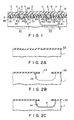
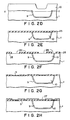
- Figs. 2A to 2O show the steps in manufacturing the field effect semiconductor device according to the embodiment of the present invention (note that the same reference numerals in Figs. 2A to 2D denote the same parts as in Fig. 1).
- a semiconductor having a first conductivity is used as a p-type silicon substrate 1, and the major surface of the p-type silicon substrate 1 is subjected to steam oxidation at a steam temperature of 1,000°C so as to form a silicon oxide film (to be referred to as an oxide film hereinafter) 22 having a thickness of about 1 ⁇ m.
- a silicon oxide film to be referred to as an oxide film hereinafter
- part of the oxide film 22 is dissolved and removed by, e.g., the photo-engraving process (PEP) to form a window 23.
- part of the silicon substrate 1 exposed in the window 23 is etched by an etching solution (HF + HNO3) using the oxide film 22 as a mask so as to form a pot-like hole 24 having a bottom and a depth of about 30 ⁇ m.
- antimony (Sb) is supplied to the surface of the hole 24 formed in the silicon substrate 1 so as to perform thermal diffusion, thus forming an n+-type silicon buried layer 9.
- the oxide film 22 is dissolved and removed by an etching solution (HF) first.
- An n ⁇ -type epitaxial growth layer 10 is formed as a semiconductor layer having a second conductivity type on the silicon substrate 1 including the hole 24 by an epitaxial growth method.
- a portion from the surface of the n ⁇ -type epitaxial growth layer 10 to the surface indicated by a line X - Y is removed by a mechanical or chemical grinding means so as to flatten the major surface of the silicon substrate 1.
- portions of the oxide film 25, which are located at prospective regions of electrodes respectively constituting an n-channel DMOS FET and a p-channel DMOS FET on the major surface of the silicon substrate 1, are selectively removed to form several windows 26.
- thermal oxidation of the silicon substrate 1 is performed to form an oxide film 5 on the oxide film 25 and the windows 26.
- the oxide film is formed by introducing dry oxygen into an atmosphere having a temperature of 1,000°C.
- a 0.5 ⁇ m thick polysilicon film 27 is formed on the oxide film 5.
- the polysilicon film 27 is selectively etched to leave only portions corresponding to gate electrodes 28 of the n-channel and p-channel DMOS-FETs. Electrodes are respectively formed at windows 29a, 29b, 29c, and 29d.
- a photoresist layer 30 is formed on the major surface of the silicon substrate 1 so as to open part of the window 29a. Subsequently, boron (B) ions are implanted in the silicon substrate 1 at an acceleration voltage of 50 keV and a dose of 1 x 1014 cm2.
- a photoresist layer 31 is formed on the silicon substrate 1 so as to open parts of the windows 29b and 29d.
- Phosphorus (P) ions are then implanted in the silicon substrate 1 at an acceleration voltage of 100 keV and a dose of 5 X 1013 cm2. In this case, peak concentration is set at about 1 x 1017 cm ⁇ 3.
- heat treatment of the silicon substrate 1 is performed in a nitrogen gas atmosphere at 1,200°C for one hour.
- the implanted boron ions are diffused in the silicon substrate 1, and an n-type silicon portion which is in contact with the oxide film 5 in the window 29a is formed into a p-type silicon region, thus forming a source region 13.
- the implanted phosphorus ions are diffused in the silicon substrate 1, and a p-type silicon portion which is in contact with the oxide film 5 in the window 29b is formed into an n-type silicon region, thus forming a source region 2.
- a p-type silicon portion which is in contact with the oxide film 5 in the window 29d is formed into an n-type silicon region, thus forming a drain region 11.
- a resist 32 is formed on the silicon substrate 1, and portions of the oxide film 5 which are in contact with the central portions of the windows 29b and 29d and both the sides of the window 29a (i.e., excluding its central portion) are selectively etched and removed. Arsenic ions are then implanted in each portion, from which the oxide film 5 is removed, so as to have a surface concentration of about 1 x 1020 cm ⁇ 3 and a junction depth XJ of 5,000 ⁇ . After the resist 32 is removed, heat treatment of the silicon substrate 1 is performed in a dry oxygen atmosphere at 1,000°C for 30 minutes.
- the implanted arsenic ions are diffused to form an n+-type silicon layer 3b in the n-type silicon region 2, an n+-type silicon layer 14a in the p-type silicon region 13, and an n+-type silicon layer 11a in the n-type silicon region 11.
- the exposed portions of the silicon layer are oxidized, and new oxide films are respectively formed on the central portion of the window 29b, on both the sides of the window 29a excluding its central portion, and in the window 29d.
- a resist 33 is formed on the silicon substrate 1 so as to open the central portion of the window 29a, both sides of the window 29b (excluding its central portion) in the p-type silicon region 2, and the drain electrode extraction portion 29c.
- boron ions are implanted to a surface concentration of about 5 X 1019 cm ⁇ 3 and a junction depth Xj of 7,000 ⁇ .
- the resist 33 is removed from the silicon substrate 1.
- a new oxide film 35 is formed on the oxide film 5 by CVD.
- heat treatment of the silicon substrate 1 is performed in a nitrogen atmosphere at 1,000°C for 20 minutes.
- the implanted boron ions are diffused to form a p+-type silicon layer 3a in the n+-type silicon layer 2, a p+-type silicon layer 14b in the p+-type silicon layer 13, and a p+-type silicon layer 7b in the drain electrode extraction portion.
- contact holes 36 are respectively formed in the gates, sources, and drains of both transistors by selective etching.
- the contact holes 36 are then filled with aluminum or an aluminum alloy, and source, gate, and drain electrodes 4, 6a, and 6b, and the like are formed on the semiconductor substrate 1.
- Heat treatment of the semiconductor substrate 1 is then performed in a nitrogen atmosphere at 400°C for 10 minutes.
- a PSG layer 17 having a thickness of about 1 ⁇ m as a top passivation layer is formed on the uppermost layer of the semiconductor substrate 1.
- the manufacturing method of the present invention allows a greater simplification of the manufacturing process and a greater reduction in the manufacturing cost of a semiconductor device than the conventional method.
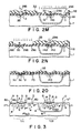
- Fig. 3 shows current paths of the field effect semiconductor device having the arrangement shown in Fig. 1.
- Fig. 3 shows a sectional portion equivalent to that of Fig. 1.
- Arrows e in Fig. 3 indicate the directions of currents.
- the same reference numerals in Fig. 3 denote the same parts as in Fig. 1.
- Each conductive body is defined by a p-type or an n-type.
- the ON resistance is reduced to 1/2 or less.
- the field effect semiconductor device described above is designed such that the p-channel DMOS FET as the first FET Q1 is formed in the p-type silicon substrate, and the n-channel DMOS FET as the second FET Q2 is formed in the n-type silicon region which is electrically isolated from the p-type silicon substrate.
- the FETs may have opposite conductivity types to those described above.
- the present invention can be equally applied to a field effect semiconductor device which is designed such that an n-channel DMOS FET as the first FET Q1 is formed on an n-type silicon substrate, and a p-channel DMOS FET as the second FET Q2 is formed in a p-type silicon region which is electrically isolated from the n-type silicon substrate by a buried layer.
- the field effect semiconductor device of the present invention is designed such that the first and second FETs Q1 and Q2 are electrically isolated from each other by one pot-like buried layer. Since only one buried layer is used, reliability of isolation is high, and the buried layer is easy to form.
- the ON resistance is reduced to 1/2 that of the conventional field effect semiconductor device or less.
- the switching speed of the circuit element is increased.
- the ON resistance can have the same value as in the conventional device, the gate width of the field effect semiconductor device of the present invention can be reduced to 1/2 that of the conventional device, thus realizing a great reduction in element area and cost.
- the source and drain regions of the first and second FETs Q1 and Q2 are simultaneously formed, two types of transistors can be efficiently formed in a single step, thus enabling simplification of the manufacturing process and a reduction in cost.
- the impurity concentration of the substrate and the impurity concentration of the epitaxial growth layer can be controlled independently of each other, thereby obtaining an impurity concentration of the drain high resistance layer, which determines the breakdown voltage of each element. Therefore, a drain high resistance layer having a high breakdown voltage can be obtained with base.
Landscapes
- Engineering & Computer Science (AREA)
- Power Engineering (AREA)
- Physics & Mathematics (AREA)
- Condensed Matter Physics & Semiconductors (AREA)
- General Physics & Mathematics (AREA)
- Computer Hardware Design (AREA)
- Microelectronics & Electronic Packaging (AREA)
- Manufacturing & Machinery (AREA)
- Metal-Oxide And Bipolar Metal-Oxide Semiconductor Integrated Circuits (AREA)
- Insulated Gate Type Field-Effect Transistor (AREA)
Applications Claiming Priority (1)
| Application Number | Priority Date | Filing Date | Title |
|---|---|---|---|
| JP63224021A JP2645100B2 (ja) | 1988-09-07 | 1988-09-07 | 電界効果型半導体装置 |
Publications (1)
| Publication Number | Publication Date |
|---|---|
| EP0445323A1 true EP0445323A1 (fr) | 1991-09-11 |
Family
ID=16807343
Family Applications (1)
| Application Number | Title | Priority Date | Filing Date |
|---|---|---|---|
| EP90104279A Withdrawn EP0445323A1 (fr) | 1988-09-07 | 1990-03-06 | Dispositif semi-conducteur à effet de champ présentant un trajet de courant formé dans une couche conductrice du substrat semi-conducteur |
Country Status (2)
| Country | Link |
|---|---|
| EP (1) | EP0445323A1 (fr) |
| JP (1) | JP2645100B2 (fr) |
Cited By (2)
| Publication number | Priority date | Publication date | Assignee | Title |
|---|---|---|---|---|
| EP0445649A3 (en) * | 1990-02-27 | 1996-03-06 | Oki Electric Ind Co Ltd | Process for producing a semiconductor substrate having therein isolated semiconductor regions |
| DE19501838A1 (de) * | 1995-01-21 | 1996-07-25 | Telefunken Microelectron | Verfahren zum Herstellen von SOI-Strukturen |
Families Citing this family (3)
| Publication number | Priority date | Publication date | Assignee | Title |
|---|---|---|---|---|
| JP2645100B2 (ja) * | 1988-09-07 | 1997-08-25 | 株式会社東芝 | 電界効果型半導体装置 |
| JP3158738B2 (ja) * | 1992-08-17 | 2001-04-23 | 富士電機株式会社 | 高耐圧mis電界効果トランジスタおよび半導体集積回路 |
| JP3711956B2 (ja) | 2002-04-01 | 2005-11-02 | 日産自動車株式会社 | 回転電機の駆動方法 |
Citations (4)
| Publication number | Priority date | Publication date | Assignee | Title |
|---|---|---|---|---|
| US4138782A (en) * | 1976-09-16 | 1979-02-13 | International Business Machines Corporation | Inverter with improved load line characteristic |
| JPS59132671A (ja) * | 1983-01-19 | 1984-07-30 | Nissan Motor Co Ltd | 縦型mosトランジスタ |
| US4566174A (en) * | 1982-10-27 | 1986-01-28 | Tokyo Shibaura Denki Kabushiki Kaisha | Semiconductor device and method for manufacturing the same |
| JPH0272662A (ja) * | 1988-09-07 | 1990-03-12 | Toshiba Corp | 電界効果型半導体装置 |
Family Cites Families (1)
| Publication number | Priority date | Publication date | Assignee | Title |
|---|---|---|---|---|
| JPS6251247A (ja) * | 1985-08-30 | 1987-03-05 | Toshiba Corp | 半導体装置及びその製造方法 |
-
1988
- 1988-09-07 JP JP63224021A patent/JP2645100B2/ja not_active Expired - Fee Related
-
1990
- 1990-03-06 EP EP90104279A patent/EP0445323A1/fr not_active Withdrawn
Patent Citations (4)
| Publication number | Priority date | Publication date | Assignee | Title |
|---|---|---|---|---|
| US4138782A (en) * | 1976-09-16 | 1979-02-13 | International Business Machines Corporation | Inverter with improved load line characteristic |
| US4566174A (en) * | 1982-10-27 | 1986-01-28 | Tokyo Shibaura Denki Kabushiki Kaisha | Semiconductor device and method for manufacturing the same |
| JPS59132671A (ja) * | 1983-01-19 | 1984-07-30 | Nissan Motor Co Ltd | 縦型mosトランジスタ |
| JPH0272662A (ja) * | 1988-09-07 | 1990-03-12 | Toshiba Corp | 電界効果型半導体装置 |
Non-Patent Citations (2)
| Title |
|---|
| PATENT ABSTRACTS OF JAPAN vol. 008, no. 261 (E - 281)<1698> 30 November 1984 (1984-11-30) * |
| PATENT ABSTRACTS OF JAPAN vol. 014, no. 252 (E - 934)<4195> 30 May 1990 (1990-05-30) * |
Cited By (2)
| Publication number | Priority date | Publication date | Assignee | Title |
|---|---|---|---|---|
| EP0445649A3 (en) * | 1990-02-27 | 1996-03-06 | Oki Electric Ind Co Ltd | Process for producing a semiconductor substrate having therein isolated semiconductor regions |
| DE19501838A1 (de) * | 1995-01-21 | 1996-07-25 | Telefunken Microelectron | Verfahren zum Herstellen von SOI-Strukturen |
Also Published As
| Publication number | Publication date |
|---|---|
| JP2645100B2 (ja) | 1997-08-25 |
| JPH0272662A (ja) | 1990-03-12 |
Similar Documents
| Publication | Publication Date | Title |
|---|---|---|
| US6194763B1 (en) | Semiconductor device having SOI-MOSFET | |
| KR100230610B1 (ko) | 자기정렬된 웰탭을 지니는 bicmos 디바이스 및 그 제조방법 | |
| EP0465961A1 (fr) | Dispositif semi-conducteur sur un substrat isolant diélectrique | |
| KR101232662B1 (ko) | 반도체 디바이스를 형성하는 방법 및 그의 구조 | |
| JPH0481337B2 (fr) | ||
| EP0248292B1 (fr) | Dispositif semi-conducteur à haute tension de claquage | |
| US4375717A (en) | Process for producing a field-effect transistor | |
| EP0091686B1 (fr) | Dispositif semi-conducteur ayant une région diffusée à longueur réduite et procédé pour la fabrication de la région | |
| EP0158292B1 (fr) | Dispositif semi-conducteur comportant un élément de circuit driver et un transistor de sortie | |
| US5506158A (en) | BiCMOS process with surface channel PMOS transistor | |
| EP0438167B1 (fr) | Dispositif à semi-conducteur avec un dispositif à transfert de charge, MOSFETs et transistors bipolaires - tous formés dans un seul substrat semi-conducteur | |
| EP0451286B1 (fr) | Dispositif à circuit intégré | |
| US4517731A (en) | Double polysilicon process for fabricating CMOS integrated circuits | |
| EP0445323A1 (fr) | Dispositif semi-conducteur à effet de champ présentant un trajet de courant formé dans une couche conductrice du substrat semi-conducteur | |
| JP3329973B2 (ja) | 半導体装置およびその製造方法 | |
| EP0402851A2 (fr) | Dispositif semi-conducteur comportant des couches d'empêchement de champ d'inversion ayant une pluralité de matériau de concentration d'impuretés selon la direction en profondeur et son procédé de fabrication | |
| JPH11340454A (ja) | 半導体装置およびその製造方法 | |
| JP3105237B2 (ja) | Dmos型半導体装置の製造方法 | |
| JP2778126B2 (ja) | 半導体装置の製造方法 | |
| JPH11330452A (ja) | 半導体装置およびその製造方法 | |
| EP0112662A1 (fr) | Dispositifs MOS empilés à interconnexions en polysilicium | |
| JPH11135783A (ja) | Mosトランジスタ及びその製造方法 | |
| JPH06151740A (ja) | パワー半導体装置 | |
| KR100209744B1 (ko) | 반도체소자 제조방법 | |
| JPH02296342A (ja) | Mosfetの製造方法 |
Legal Events
| Date | Code | Title | Description |
|---|---|---|---|
| PUAI | Public reference made under article 153(3) epc to a published international application that has entered the european phase |
Free format text: ORIGINAL CODE: 0009012 |
|
| 17P | Request for examination filed |
Effective date: 19900306 |
|
| AK | Designated contracting states |
Kind code of ref document: A1 Designated state(s): DE FR GB |
|
| STAA | Information on the status of an ep patent application or granted ep patent |
Free format text: STATUS: THE APPLICATION HAS BEEN WITHDRAWN |
|
| 18W | Application withdrawn |
Withdrawal date: 19921209 |