EP0444925A2 - Bildstabilisierungsschaltung - Google Patents
Bildstabilisierungsschaltung Download PDFInfo
- Publication number
- EP0444925A2 EP0444925A2 EP91301634A EP91301634A EP0444925A2 EP 0444925 A2 EP0444925 A2 EP 0444925A2 EP 91301634 A EP91301634 A EP 91301634A EP 91301634 A EP91301634 A EP 91301634A EP 0444925 A2 EP0444925 A2 EP 0444925A2
- Authority
- EP
- European Patent Office
- Prior art keywords
- signals
- section
- circuit
- synchronising
- output
- Prior art date
- Legal status (The legal status is an assumption and is not a legal conclusion. Google has not performed a legal analysis and makes no representation as to the accuracy of the status listed.)
- Granted
Links
- 230000003019 stabilising effect Effects 0.000 title claims abstract description 19
- 238000000926 separation method Methods 0.000 claims abstract description 32
- 238000000034 method Methods 0.000 claims abstract description 11
- 230000001629 suppression Effects 0.000 claims description 13
- 230000008929 regeneration Effects 0.000 claims description 10
- 238000011069 regeneration method Methods 0.000 claims description 10
- 239000003990 capacitor Substances 0.000 claims description 3
- 230000010354 integration Effects 0.000 claims 2
- 230000000903 blocking effect Effects 0.000 claims 1
- 239000003086 colorant Substances 0.000 description 3
- 230000003111 delayed effect Effects 0.000 description 2
- 238000010586 diagram Methods 0.000 description 2
- 238000006243 chemical reaction Methods 0.000 description 1
- 238000001514 detection method Methods 0.000 description 1
- 230000009977 dual effect Effects 0.000 description 1
- 238000000605 extraction Methods 0.000 description 1
- 230000008570 general process Effects 0.000 description 1
- 230000007274 generation of a signal involved in cell-cell signaling Effects 0.000 description 1
- 238000002955 isolation Methods 0.000 description 1
- 238000004519 manufacturing process Methods 0.000 description 1
- 230000008569 process Effects 0.000 description 1
- 230000000153 supplemental effect Effects 0.000 description 1
- 230000001960 triggered effect Effects 0.000 description 1
Images


Classifications
-
- H—ELECTRICITY
- H04—ELECTRIC COMMUNICATION TECHNIQUE
- H04N—PICTORIAL COMMUNICATION, e.g. TELEVISION
- H04N9/00—Details of colour television systems
- H04N9/64—Circuits for processing colour signals
- H04N9/641—Multi-purpose receivers, e.g. for auxiliary information
Definitions
- the present invention relates to a picture regeneration stabilising circuit, and particularly to the operation of such a circuit during a non-signal input (non-inputting)or blanking period in order to stabilise the colours of the picture by preventing discrimination errors caused by gating noise when discriminating the broadcasting method during tape regeneration (playback).
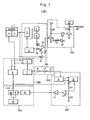
- tuner video signals b which are selected through a switching section 1 in order to switch the tuner line video input, are supplied to a low pass filter 2.
- This low pass filter 2 is a component of a tuner synchronizing separation section 100 which includes the low pass filter 2, a synchronizing isolator 3, a horizontal automatic frequency control section 4, a horizontal oscillator 5, inverters 3A, A, A′, and an AND gate 16.
- the signals which are filtered through the low pass filter 2 are simultaneously supplied to both the synchronizing isolator 3 and the horizontal automatic frequency control section 4.
- the output of the horizontal automatic frequency control section 4 is supplied to the horizontal oscillator 5 in order to control the horizontal synchronizing signal generation, and the horizontal synchronizing signals which are generated through the horizontal oscillator 5 are supplied to an input terminal of the AND gate 16.
- the synchronizing signals which are isolated through the synchronizing isolator 3 are supplied to another input terminal of the AND gate 16 where the signals of the horizontal oscillator 5 are supplied through the other input terminal.
- the output of the AND gate 16 is supplied to the base of a transistor Q2 of a modulator video input muter (suppression) circuit 200 which includes transistors Q2-Q5, and which is for preventing tuner/line interference.
- the output of the AND gate 16 is supplied through the inverter A to the input terminal of the inverter A′, and the output of the inverter A′ is supplied to both a chroma drive 8 and a low pass filter 6 of a Y/C (brightness/colour) separation section 300.
- the section 300 includes the low pass filter 6, the chroma drive 8 and a synchronizing isolator 7, and is connected to the tuner video b.
- a discriminating section 400 which includes a B.G.P. delaying detecting section 11, a burst gate 12, an OP amplifier OP1 and a buffer 13 is supplied to the PAL/MESECAM detection section 10.
- the output of the delay section 500 is also supplied to the input terminal of the B.G.P. delaying detecting section 11, while the output of the B.G.P. delaying detecting section 11 is supplied to the burst gate 12.
- the output signals of the chroma drive section 8, which is for extracting the colour signals from the synchronizing signals supplied to the Y/C separation section 300, are supplied to the burst gate 12.
- the output of the burst gate 12 is supplied to the OP amplifier OP1 which carries out a comparison with the reference voltage as determined by resistances R7,R8.
- the output of the OP amplifier OP1 is supplied through the buffer 13 to a PAL/MESECAM detecting section 10 of a broadcasting method discriminating section 700 which includes a phase detecting section 18, a recognition signal (ID) detecting section 9 and a colour killer 19 in addition to the PAL/MESECAM detecting section 10.
- the output of the PAL/MESECAM detecting section 10 is supplied to both the recognition (ID) signal detecting section 9 and the phase detecting section 18.
- the recognition signal and phase detecting sections 9, 18 are connected to the colour killer 19, and the line video output 'a' which is selected by the switching device 1 is also supplied to both the low pass filter 6 and the chroma drive section 8 of the Y/C separation section 300.
- the modulator video input muter circuit 200 receives through its base the output of the AND gate 16 of the tuner synchronizing separation section 100, and the emitter of the transistor Q2 of the section 200 is grounded.
- the collector of the transistor Q2 is connected to both the emitter of the transistor Q3 and the resistance R9 where the power source Vcc is supplied.
- the base of the transistor Q3 is connected to the collector of the transistor Q4 which is grounded through its emitter and receives through its base the tuner high signals from a microcomputer.
- the collector of the transistor Q3 is connected to the base of the transistor Q5 which is grounded through its emitter.
- the collector of the transistor Q5 is connected through a capacitor C4 to a video input terminal IN, and also connected ultimately to a modulator 17.
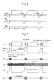
- the mode switching device 1 of Figure 1 under the condition that the mode switching device 1 of Figure 1 is selected, if a tuner video signal b is supplied to the tuner synchronizing separation section 100, the colour or chroma signals C are removed by the low pass filter 2, and only the signals (the wave pattern 1 of Figure 2) of the pure brightness or luminance component Y are supplied to both the synchronizing isolator 3 and the horizontal automatic frequency control section 4.
- the synchronizing signals are isolated by the synchronizing isolator 3, and the isolated signals pass through the inverter 3a with the result that the signals take the wave pattern 4 of Figure 2, and that they are supplied to one of the input terminals B of the AND gate 16.
- a saw tooth wave (wave pattern 3 of Figure 2) is generated by the frequency (15 ⁇ 62 KHz) of the horizontal automatic frequency control section 4, and therefore, the horizontal synchronizing signals generated from the horizontal synchronizing oscillator 5 are continuously triggered in such a manner that they exactly correspond to 64 microseconds. Then these signals are supplied to the other input terminal A of the AND gate 16 in the form of the wave pattern 2 of Figure 2.
- the AND gate 16 compares the two inputs A,B, and if the two inputs A,B are in a high state (that is, if it is the normal state in which video signals are received under the actual tuner mode), a high state output is produced and supplied to the base of the transistor Q2, so that transistor Q2 is turned on. Consequently, the potential of the collector of the transistor Q2 goes low and this low state is supplied to the emitter of the transistor Q3.
- the transistor Q4 which receives a high signal from the micom is turned on in its collector and emitter so as for the collector of the transistor Q4 to have a low state before being supplied to the base of the power source driven transistor Q3.
- the transistor Q3 is turned off because of the low state of the emitter, and therefore, a low potential is supplied to the base of the transistor Q5 which is used in muting the inputted video signals of the final modulator 17.
- the transistor Q5 is also turned off, so that video signals should be output through the modulator 17 in a normal manner.
- the high output of the AND gate 16 sequentially passes through the inverters A,A′, and therefore, muting is not carried out for the input video signals of the Y/C isolating section 300, with the result that the video signals are inputted into the Y/C isolating section 300 in a normal manner.
- a colour signal C having the form of the wave pattern 1 of Figure 3 is supplied to the burst gate 12 of the discriminating section 400 by the chroma drive 8 of the Y/C isolating section 300, and consequently, colour burst and recognition signal gate portions are detected in the form of the wave pattern 3 of Figure 3 in the burst gate 12 by the BGP signals which are output from the BGP delaying detecting section 11 (PAL signals do not have frequency deviations, but MESECAM signals do).
- the signals are supplied to the OP amplifier OP1 where the signals are compared with the reference voltages of the supply resistances R7,R8.
- the signals are supplied through the output buffer 13 of the OP amplifier OP1 to the PAL/MESECAM detecting section 10 of a broadcasting method discriminating section 700, and the PAL/MESECAM detecting section 10 is controlled by the output of the OP amplifier OP1 which is output through the buffer 13 (the output being low in the case of PAL, and the output being high in the case of MESECAM).
- the signals are detected by the phase detecting section 18 in the case of PAL signals, and by the recognition signal detecting section 9 in the case of MESECAM signals.
- the requirement for colour killing is decided in the conventional manner by the colour killer 19, and the colour signals are output after undergoing conventional processes and after being Y/C-mixed.
- the synchronising signals of the synchronising isolator 3 of the Y/C isolating section 300 may include just the synchronising signals or, alternatively, both the synchronising signals and the BGP signals (refer to the wave pattern 2 of Figure 3), depending on the type of IC.
- the description is given based on the assumption that both the synchronising signals and the BGP signals are simultaneously obtained.
- the output of the AND gate 16 is shifted to a low state, with the result that the transistor Q2 of the muting circuit 200 is turned off, and that the transistors Q3, Q4,Q5 are turned on.
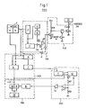
- the line video is also subjected to the extraction of the brightness signals Y by the low pass filter 6 as in the case of the tuner video input.
- synchronising (B.G.P) isolation is carried out by the synchronising isolator 7, and then a delay is introduced by the delay section 500 before being supplied to the discriminating section 400.
- the line video colour signals are supplied to the discriminating section 400 by the chroma driver section 8 after going through the general processes, and the discriminating section 400 is operated in the same manner as when processing the tuner video signals.
- the output of the section 400 is supplied to the Y/C isolating section 300 which outputs it in the form of video signals.
- the B.G.P signals will be described as a supplemental matter. That is, the B.G.P signals are needed for the following reason.
- the discriminating section 400 carries out discriminating errors, and therefore, the colour killer 19 has to be operated until the B.G.P and colour signals are normally operated, or delay or distortion of colours will appear.
- a synchronising signal (or a high signal) is output from the internal circuit in order to carry out video suppression through the inverters A,A′.
- noise is produced which is similar in form to a synchronising signal, it is mistaken for a video signal, and therefore, in spite of the fact that there is no video signal, suppression cannot be perfectly carried out, with the result that the picture on the screen is distorted and so on.
- a picture stabilising circuit for stabilising a picture signal particularly during non-signal input, comprising: a tuner synchronising separation section for receiving tuner video signals; a video suppression circuit to be controlled by the output of the tuner synchronising separation section and for preventing tuner/line interferences; a Y/C separation section for receiving tuner/line video signals and carrying out Y/C separation; a discriminating section for receiving synchronising signals and the chroma signals separated by the Y/C separation section, detecting colour burst signals and recognition signals and carrying out a comparison with a reference voltage to produce an output; and a broadcasting method discriminating section for discriminating and selecting the broadcasting method based on the output of the discriminating section,
- the stabilising circuit further comprises: a further suppression circuit for muting the chroma signals and the synchronising signals supplied to the discriminating section during non-signal input.
- the present invention is intended to overcome the above described disadvantages of the conventional circuit by the provision of a picture regeneration stabilising circuit with dual suppression circuits.
- the further suppression circuit is controlled by the output of a synchronising signal isolator of the Y/C separation section, and the Y/C separation section is adapted to output synchronising signals (B.G.P.) in the presence of a line/tuner video signal input, and to output a high voltage in the absence of such input signals.
- a synchronising signal isolator of the Y/C separation section is adapted to output synchronising signals (B.G.P.) in the presence of a line/tuner video signal input, and to output a high voltage in the absence of such input signals.
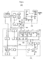
- the present invention provides an improvement of the conventional circuit in a manner described below. That is, the synchronising signals (B.G.P.) output from the synchronising isolator 7 of the Y/C separation section 300 are supplied through integrating and dc flattening circuits d,e,f (respectively consisting of a resistance and a capacitor) and through a resistance R4 to the transistor Q1.
- the emitter of the transistor Q1 is grounded, and the collector of the transistor Q1 is connected through a resistance R5 to the delay section 500, and to the output terminal of the chroma drive section 8 which is connected to the burst gate 12.
- the wave pattern 1 (SYNC+ B.G.P. signals) of Figure 5 is output from the synchronising isolator 7.
- the synchronising signals (B.G.P.) having the form of the wave pattern 1 of Figure 5 successively pass through the integrating circuit d consisting of resistance R1 and a capacitance C1, the integrating circuit e consisting of a resistance R2 and a capacitance C2, and the integrating circuit f consisting of a resistance R3 and a capacitance C3.
- the signals take the wave pattern 2 of Figure 5, and are supplied to the base of the synchronising (B.G.P.) colour suppressing transistor Q1.
- the signals supplied as described above will behave in such a manner that the synchronising (B.G.P.) signals and the chroma signals which have passed respectively through the delay section 500 and the chroma drive section 8 will be supplied to the discriminating section 400 in the normal manner, because the supplied signal (wave pattern 2 of Figure 5) corresponds to (lies below) the active reference level of the transistor Q1, and consequently the transistor Q1 is turned off.
- a high voltage is output instead of a synchronising (B.G.P.) signal from the synchronising isolator 7 of the Y/C separation section 300 (when there is no signal input, the power source voltage is output because of the inherent nature of the synchronising isolator).
- This high voltage is supplied to the base of the synchronising (B.G.P.) and colour muting transistor Q1 in the form of the wave pattern 6 of Figure 5, after passing through the integrating circuits d,e,f consisting respectively of resistance R1, capacitance C1, resistance R2, capacitance C2, resistance R3 and capacitance C3.
- the synchronising signals (B.G.P.) are suppressed in the form of the wave pattern 4 of Figure 5, and consequently, the noise component having the form of the wave pattern 3 of Figure 5 and supplied from the chroma drive section 8 during the drum loading at the initial regeneration is not gated.
- the synchronising signals are delayed up to the colour burst and ID pulse positions, so that erroneous outputs of the discriminating section may be prevented, thereby making it possible to discriminate between PAL, MESECAM and SECAM. (Refer to the dotted synchronisation pulses, a′, of the wave pattern 7 of Figure 5). That is, according to embodiments of the present invention, during non-signal input or blanking periods, the high voltage output from the synchronising isolator is utilized in order to drive the suppression transistor Q1, so that the noise which would otherwise be input into the burst gate 12 is eliminated, thereby stabilising the regenerated picture.
Landscapes
- Engineering & Computer Science (AREA)
- Multimedia (AREA)
- Signal Processing (AREA)
- Processing Of Color Television Signals (AREA)
Applications Claiming Priority (2)
| Application Number | Priority Date | Filing Date | Title |
|---|---|---|---|
| KR900002373 | 1990-02-28 | ||
| KR237390 | 1990-02-28 |
Publications (3)
| Publication Number | Publication Date |
|---|---|
| EP0444925A2 true EP0444925A2 (de) | 1991-09-04 |
| EP0444925A3 EP0444925A3 (en) | 1993-05-19 |
| EP0444925B1 EP0444925B1 (de) | 1997-02-05 |
Family
ID=19296401
Family Applications (1)
| Application Number | Title | Priority Date | Filing Date |
|---|---|---|---|
| EP19910301634 Expired - Lifetime EP0444925B1 (de) | 1990-02-28 | 1991-02-28 | Bildstabilisierungsschaltung |
Country Status (1)
| Country | Link |
|---|---|
| EP (1) | EP0444925B1 (de) |
Family Cites Families (2)
| Publication number | Priority date | Publication date | Assignee | Title |
|---|---|---|---|---|
| FR2428362A1 (fr) * | 1978-06-09 | 1980-01-04 | Thomson Csf | Circuit de decodage des informations de chrominance, dans le systeme de television secam, et recepteur de television comportant un tel circuit |
| JPS62227291A (ja) * | 1986-03-29 | 1987-10-06 | Toshiba Corp | 自動色飽和度制御装置 |
-
1991
- 1991-02-28 EP EP19910301634 patent/EP0444925B1/de not_active Expired - Lifetime
Also Published As
| Publication number | Publication date |
|---|---|
| EP0444925A3 (en) | 1993-05-19 |
| EP0444925B1 (de) | 1997-02-05 |
Similar Documents
| Publication | Publication Date | Title |
|---|---|---|
| CA1252880A (en) | Multi-system television receiver | |
| EP0084241B1 (de) | Gerät zur Signalverarbeitung und Verfahren zum Aufzeichnen auf einem Videoband | |
| EP0173439B1 (de) | Luminanz-Chrominanzsignal-Trennstufe | |
| JPH0566076B2 (de) | ||
| US4847682A (en) | Adaptive comb filter for artifact-free decoding | |
| EP0444925B1 (de) | Bildstabilisierungsschaltung | |
| EP0342634A2 (de) | Schaltungsanordnung und Methode zur Erzeugung eines vertikalen Treiberimpulses in einem Videosignalempfänger | |
| US4015287A (en) | Color television receiver including a chrominance subcarrier regenerator | |
| JP3092938B2 (ja) | 画像表示装置用ディジタル同期回路 | |
| US5815213A (en) | Video signal synchronization extraction device | |
| US7777813B2 (en) | Color burst automatic detection device | |
| JP2619524B2 (ja) | ゴースト検出用基準信号の抽出回路 | |
| KR910005705Y1 (ko) | Pal/secam방식의 자동 색신호 제거회로 | |
| KR100395698B1 (ko) | 텔레비젼수상기 | |
| KR900000126B1 (ko) | 다중시스템 텔레비젼 수신기 | |
| US7432918B2 (en) | Video signal processing circuit | |
| KR940011032B1 (ko) | 자동 선국 구동장치 | |
| JPH0723304A (ja) | 映像信号選択回路の信号検出回路 | |
| JPS5825779A (ja) | 多方式カラ−テレビジヨン受像機 | |
| JP3110196B2 (ja) | クシ型フィルタ自動調整回路 | |
| JPS628628Y2 (de) | ||
| JP2604424B2 (ja) | 同期分離回路 | |
| CA1262281A (en) | Multi-system television receiver | |
| US5122867A (en) | Video signal processing circuit having a band pass filter following a delay circuit in a comb filter arrangement | |
| KR920001109B1 (ko) | Vdp정지신호 검출회로 |
Legal Events
| Date | Code | Title | Description |
|---|---|---|---|
| PUAI | Public reference made under article 153(3) epc to a published international application that has entered the european phase |
Free format text: ORIGINAL CODE: 0009012 |
|
| AK | Designated contracting states |
Kind code of ref document: A2 Designated state(s): DE FR GB |
|
| PUAL | Search report despatched |
Free format text: ORIGINAL CODE: 0009013 |
|
| AK | Designated contracting states |
Kind code of ref document: A3 Designated state(s): DE FR GB |
|
| 17P | Request for examination filed |
Effective date: 19930908 |
|
| 17Q | First examination report despatched |
Effective date: 19950818 |
|
| GRAG | Despatch of communication of intention to grant |
Free format text: ORIGINAL CODE: EPIDOS AGRA |
|
| GRAH | Despatch of communication of intention to grant a patent |
Free format text: ORIGINAL CODE: EPIDOS IGRA |
|
| GRAH | Despatch of communication of intention to grant a patent |
Free format text: ORIGINAL CODE: EPIDOS IGRA |
|
| GRAA | (expected) grant |
Free format text: ORIGINAL CODE: 0009210 |
|
| AK | Designated contracting states |
Kind code of ref document: B1 Designated state(s): DE FR GB |
|
| REF | Corresponds to: |
Ref document number: 69124535 Country of ref document: DE Date of ref document: 19970320 |
|
| ET | Fr: translation filed | ||
| PLBE | No opposition filed within time limit |
Free format text: ORIGINAL CODE: 0009261 |
|
| STAA | Information on the status of an ep patent application or granted ep patent |
Free format text: STATUS: NO OPPOSITION FILED WITHIN TIME LIMIT |
|
| 26N | No opposition filed | ||
| REG | Reference to a national code |
Ref country code: GB Ref legal event code: IF02 |
|
| PGFP | Annual fee paid to national office [announced via postgrant information from national office to epo] |
Ref country code: FR Payment date: 20100223 Year of fee payment: 20 |
|
| PGFP | Annual fee paid to national office [announced via postgrant information from national office to epo] |
Ref country code: GB Payment date: 20100224 Year of fee payment: 20 Ref country code: DE Payment date: 20100312 Year of fee payment: 20 |
|
| REG | Reference to a national code |
Ref country code: DE Ref legal event code: R071 Ref document number: 69124535 Country of ref document: DE |
|
| REG | Reference to a national code |
Ref country code: GB Ref legal event code: PE20 Expiry date: 20110227 |
|
| PG25 | Lapsed in a contracting state [announced via postgrant information from national office to epo] |
Ref country code: GB Free format text: LAPSE BECAUSE OF EXPIRATION OF PROTECTION Effective date: 20110227 |
|
| PG25 | Lapsed in a contracting state [announced via postgrant information from national office to epo] |
Ref country code: DE Free format text: LAPSE BECAUSE OF EXPIRATION OF PROTECTION Effective date: 20110228 |