EP0442801A2 - Procédé de fabrication d'un filtre diélectrique à couches multiples - Google Patents
Procédé de fabrication d'un filtre diélectrique à couches multiples Download PDFInfo
- Publication number
- EP0442801A2 EP0442801A2 EP91400346A EP91400346A EP0442801A2 EP 0442801 A2 EP0442801 A2 EP 0442801A2 EP 91400346 A EP91400346 A EP 91400346A EP 91400346 A EP91400346 A EP 91400346A EP 0442801 A2 EP0442801 A2 EP 0442801A2
- Authority
- EP
- European Patent Office
- Prior art keywords
- dielectric multilayer
- fluorinated polyimide
- multilayer filter
- optical
- filter
- Prior art date
- Legal status (The legal status is an assumption and is not a legal conclusion. Google has not performed a legal analysis and makes no representation as to the accuracy of the status listed.)
- Granted
Links
Images


Classifications
-
- G—PHYSICS
- G02—OPTICS
- G02B—OPTICAL ELEMENTS, SYSTEMS OR APPARATUS
- G02B5/00—Optical elements other than lenses
- G02B5/20—Filters
- G02B5/28—Interference filters
- G02B5/285—Interference filters comprising deposited thin solid films
-
- G—PHYSICS
- G02—OPTICS
- G02B—OPTICAL ELEMENTS, SYSTEMS OR APPARATUS
- G02B6/00—Light guides; Structural details of arrangements comprising light guides and other optical elements, e.g. couplings
- G02B6/10—Light guides; Structural details of arrangements comprising light guides and other optical elements, e.g. couplings of the optical waveguide type
- G02B6/12—Light guides; Structural details of arrangements comprising light guides and other optical elements, e.g. couplings of the optical waveguide type of the integrated circuit kind
- G02B6/12007—Light guides; Structural details of arrangements comprising light guides and other optical elements, e.g. couplings of the optical waveguide type of the integrated circuit kind forming wavelength selective elements, e.g. multiplexer, demultiplexer
-
- G—PHYSICS
- G02—OPTICS
- G02B—OPTICAL ELEMENTS, SYSTEMS OR APPARATUS
- G02B6/00—Light guides; Structural details of arrangements comprising light guides and other optical elements, e.g. couplings
- G02B6/24—Coupling light guides
- G02B6/26—Optical coupling means
- G02B6/28—Optical coupling means having data bus means, i.e. plural waveguides interconnected and providing an inherently bidirectional system by mixing and splitting signals
- G02B6/293—Optical coupling means having data bus means, i.e. plural waveguides interconnected and providing an inherently bidirectional system by mixing and splitting signals with wavelength selective means
- G02B6/29346—Optical coupling means having data bus means, i.e. plural waveguides interconnected and providing an inherently bidirectional system by mixing and splitting signals with wavelength selective means operating by wave or beam interference
- G02B6/29361—Interference filters, e.g. multilayer coatings, thin film filters, dichroic splitters or mirrors based on multilayers, WDM filters
- G02B6/2937—In line lens-filtering-lens devices, i.e. elements arranged along a line and mountable in a cylindrical package for compactness, e.g. 3- port device with GRIN lenses sandwiching a single filter operating at normal incidence in a tubular package
-
- G—PHYSICS
- G02—OPTICS
- G02B—OPTICAL ELEMENTS, SYSTEMS OR APPARATUS
- G02B6/00—Light guides; Structural details of arrangements comprising light guides and other optical elements, e.g. couplings
- G02B6/24—Coupling light guides
- G02B6/26—Optical coupling means
- G02B6/28—Optical coupling means having data bus means, i.e. plural waveguides interconnected and providing an inherently bidirectional system by mixing and splitting signals
- G02B6/293—Optical coupling means having data bus means, i.e. plural waveguides interconnected and providing an inherently bidirectional system by mixing and splitting signals with wavelength selective means
- G02B6/29379—Optical coupling means having data bus means, i.e. plural waveguides interconnected and providing an inherently bidirectional system by mixing and splitting signals with wavelength selective means characterised by the function or use of the complete device
- G02B6/2938—Optical coupling means having data bus means, i.e. plural waveguides interconnected and providing an inherently bidirectional system by mixing and splitting signals with wavelength selective means characterised by the function or use of the complete device for multiplexing or demultiplexing, i.e. combining or separating wavelengths, e.g. 1xN, NxM
-
- G—PHYSICS
- G02—OPTICS
- G02B—OPTICAL ELEMENTS, SYSTEMS OR APPARATUS
- G02B6/00—Light guides; Structural details of arrangements comprising light guides and other optical elements, e.g. couplings
- G02B6/10—Light guides; Structural details of arrangements comprising light guides and other optical elements, e.g. couplings of the optical waveguide type
- G02B6/12—Light guides; Structural details of arrangements comprising light guides and other optical elements, e.g. couplings of the optical waveguide type of the integrated circuit kind
- G02B2006/12083—Constructional arrangements
- G02B2006/12109—Filter
-
- Y—GENERAL TAGGING OF NEW TECHNOLOGICAL DEVELOPMENTS; GENERAL TAGGING OF CROSS-SECTIONAL TECHNOLOGIES SPANNING OVER SEVERAL SECTIONS OF THE IPC; TECHNICAL SUBJECTS COVERED BY FORMER USPC CROSS-REFERENCE ART COLLECTIONS [XRACs] AND DIGESTS
- Y10—TECHNICAL SUBJECTS COVERED BY FORMER USPC
- Y10T—TECHNICAL SUBJECTS COVERED BY FORMER US CLASSIFICATION
- Y10T428/00—Stock material or miscellaneous articles
- Y10T428/31504—Composite [nonstructural laminate]
- Y10T428/31721—Of polyimide
Definitions
- the present invention pertains to filters employed in optical communication systems, and more particularly, to dielectric multilayer interference filters for optical communication systems and to components which incorporate such filters.
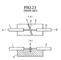
- Fig. 23 shows a conventional optical element in which a dielectric multilayer filter is interposed between the end of one optical fiber and that of another, as described by H. Yanagawa et al. ("Filter-Embedded Design and its Applications to Passive Components", IEEE J. Lightwave Technol., vol. LT-7, pp. 1646-53, 1989).
- Fig. 23(a) is a plan view of the optical element, and Fig.
- FIG. 23(b) is a vertical cross-sectional view of the optical element through the line A - A′ shown in Fig. 23(a).
- the ends of an input optical fiber 1 and an output optical fiber 2 can be seen opposing one another with an intervening dielectric multilayer filter leaf 3 which is situated within a slot 4 formed in a support base 5.
- support base 5 also supports and fixes the ends of the above mentioned input optical fiber 1 and output optical fiber 2.
- dielectric multilayer filter leaf 3 having suitable optical characteristics, and appropriately adjusting the angle between dielectric multilayer filter leaf 3 and the optical axis of the optical element as determined by the orientation of the above mentioned groove 4 in support base 5, it is possible to fabricate an optical element which transmits light at one wavelength, and which reflects, and hence blocks, light at another wavelength.
- an input optical fiber 1 in which light propagating therein includes a component having a wavelength given by ⁇ 1 and a second component having a wavelength given by ⁇ 2, where light at wavelength ⁇ 1 is necessary for operation of the optical communication system and light at wavelength ⁇ 2 is of no use or possibly undesirable, the wavelength ⁇ 2 component can be selectively blocked by means of the optical element, whereas the wavelength ⁇ 1 component is transmitted on to the output optical fiber 2 to propagate therein.
- light that is reflected backwards at the dielectric multilayer filter leaf 3 and reenters the input optical fiber 1 escapes therefrom via the cladding layer thereof.
- This rearward reflection can be maximized by carefully choosing the angle formed between the plane in which the dielectric multilayer filter leaf 3 lies and the optical axis of the optical element. It view of the above discussion, it can be seen that this type of optical element effectively transforms output optical fiber 2 into a filtered input optical fiber.
- an optical fiber is fixed in a groove provided in support base 5 using an optical adhesive agent so as to extend beyond either end of support base 5, the above mentioned groove being parallel to the optical axis of the optical element to be fabricated.
- a groove is formed in support base 5 which intersects with the optical axis of the optical element, and forms a predetermined angle therewith.
- the dielectric multilayer filter leaf 3 is then fixed in this groove, again using an optical adhesive agent.
- the optical element of Fig. 23 as described above consists of a single, linear optical pathway with an intervening dielectric multilayer filter.
- other types of optical elements are conventionally known which employ dielectric multilayer filters.
- Examples of optical elements to which the application of one or more dielectric multilayer filters have been considered include multiple pathway optically coupling-splitting devices, wherein two or more optical fibers are brought into close approximation with one another in a parallel arrangement over a portion of their lengths to form an optical coupling region, whereby wavelength dependent optical coupling is achieved.
- the wavelength dependent coupling ratio between a pair of component optical fibers in the coupling region can be adjusted, whereby a desired distribution of outgoing light over two or more output optical fibers can be effected, thereby achieving splitting of one or more input optical signals into different wavelength components thereof.
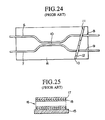
- FIG. 24 one example of the above described type of multiple pathway optically coupling-splitting device is shown, wherein two dielectric multilayer filters are incorporated.
- the optical element shown in Fig. 24 includes two input optical fibers 6, 7, two output optical fibers 8, 9, an optical coupling region 10, two dielectric multilayer filter leaves 11, 12, a groove 13 wherein dielectric multilayer filter leaves 11 and 12 are inserted, and a base support 14 whereby input optical fibers 6 and 7, output optical fibers 8 and 9 and dielectric multilayer filter leaves 11 and 12 are supported.
- the coupling ratio between component optical fibers in the coupling region of this kind of device is known to be wavelength dependent.
- optical coupling portion 10 when an optical signal having two different wavelength components is supplied to optical coupling portion 10 via input optical fiber 6, depending on the wavelength of each component, and on the wavelength dependent characteristics of optical coupling region 10, it is possible to effect a substantial separation of the two wavelength components, such that a large proportion of one wavelength component is output from the optical element via dielectric multilayer filter leaf 11 and output optical fiber 8, and a large proportion of the other wavelength component is output from the optical element via dielectric multilayer filter leaf 12 and output optical fiber 9. In other words, splitting of the incoming optical signal into individual wavelength components thereof is achieved. Because it is not practical to achieve complete separation of the individual wavelength components of the input optical signal by means of the coupling region alone, in the device shown in Fig.
- dielectric multilayer filter leaf 11 is incorporated into one of the outgoing pathways, and dielectric multilayer filter leaf 12 is incorporated into the other, whereby the effectiveness of separation according to wavelength can be improved.
- dielectric multilayer filter leaf 12 is incorporated into the other, whereby the effectiveness of separation according to wavelength can be improved.
- diffraction may occur in the groove in which the dielectric multilayer filter leaves are mounted, thereby leading to a broadening of the intensity distribution, and hence optical losses. It is possible, however, to limit such optical losses by limiting the thickness of the groove for the dielectric multilayer filter leaves, that is, the length of the optical pathway which lies in the groove.
- the thickness of the groove for the dielectric multilayer filter leaves that is, the length of the optical pathway which lies in the groove.
- a groove thickness on the order of tens of ⁇ m or less it is possible to limit diffraction losses which occur at the interstice between the input optical fiber and the output optical fiber to on the order of 0.5 dB. From the above, it can be seen that a correspondingly thin dielectric multilayer filter leaf is necessary to limit diffraction losses.
- conventional dielectric multilayer filters consist of a hard base layer 15 with an overlying dielectric multilayer 16.
- the base layer 15 must be transparent, and must possess smooth surfaces and sufficient mechanical strength. For this reason, optical flat plate glass is often employed, for example, synthetic quartz glass, BK-7, etc., with a thickness of 0.5 mm or greater.
- the dielectric multilayer 16 consists of alternating low refractive index layers 17 and high refractive index layers 18. In addition to alternating low refractive index layers 17 and high refractive index layers 18, the dielectric multilayer 16 may also incorporate one or more additional layers having an intermediate refractive index between each pair of low refractive index and high refractive index layers 17, 18.
- the thickness thereof is great to the extent that wavelengths it must handle are long. Additionally, in order to provide the required spectral characteristics, a fairly large number of individual component layers is necessary. In the case of fiber optic communication systems, the wavelength of light employed therein is ordinarily in the range of from 1.31 to 1.55 ⁇ m, for which reason, the thickness of the dielectric multilayer 16 may reach 10 ⁇ m in order to provide suitable spectral characteristics. As mentioned previously, the base layer 15 initially has a thickness of 0.5 mm or greater.
- the second shortcoming relates to the fact that conventional ion assist vapor deposition methods are employed so as to provide a dielectric multilayer with highly uniform wavelength dependent optical characteristics.
- ion assist vapor deposition methods are employed so as to provide a dielectric multilayer with highly uniform wavelength dependent optical characteristics.
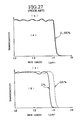
- Examination of the graph of Fig. 26 will help to clarify the above point.
- Fig. 26 displays actual measurements taken using a talystep from the upper surface of the dielectric multilayer of two dielectric multilayer filters.
- the curve labeled A is from a dielectric multilayer filter which was subjected to ion assist processing
- the line labeled B is from a dielectric multilayer filter which was not subjected to ion assist processing, but rather, underwent conventional vapor deposition.
- Both the dielectric multilayer filter corresponding to curve A, and the dielectric multilayer filter corresponding to line B included a base layer of 0.5 mm thick BK-7 glass, and the dielectric multilayer of each had a thickness of approximately 10 ⁇ m and was made up of alternating layers of TiO2 and SiO2 for the purpose of separating an input signal into a 1.3 ⁇ m wavelength component and a 1.55 ⁇ m wavelength component.
- the dielectric multilayer filter corresponding to curve A developed marked curling with a large central protuberance.
- dielectric multilayer filters manufactured using conventional vapor deposition are more resistant to warping secondary to internal residual stress
- dielectric multilayer filters manufactured using ion assist processing are more resistant to water vapor, and hence, more stable under conditions of varying humidity.
- dielectric multilayer filters Because of the exceptional expense involved in producing dielectric multilayer filters by conventional methods which require reduction of thickness by grinding and polishing, the present inventors investigated methods whereby it is possible to produce such filters having the desired thickness from the onset without need of such treatment.
- dielectric multilayer filters consisting of a plastic film base layer, over which a multilayer interference membrane is applied, such as those disclosed by Sugiyama et al. (Japanese Patent Application, First Publication Serial No. Sho-63-64003), and that of J. A. Dobrowolski et al. ( Applied Optics , vol. 28, no. 14, pp. 2702).
- the filters of both of the above two cited references were had a multilayer interference membrane consisting of on the order of twenty individual layers, each individual layer approximately 0.2 ⁇ m thick.
- the filters of the former reference are produced by the socalled roll application method and are stored in roll form after manufacture thereof.
- Such filters have a rather nonuniform thickness of the multilayer interference membrane, and the multilayer interference membrane is prone to cracking and peeling away from the base layer under storage conditions.
- a polyester film base layer having a thickness of 100 ⁇ m is employed in order to provide adequate mechanical strength.
- the present inventors investigated using a thin plastic film polyimide layer which is applied over a conventional base layer of glass or the like, followed by application of the multilayer structure using an ion assist method, after which the resulting product is stripped away from the underlying glass layer.
- the material for the thin plastic film polyimide layer was selected so as to provide a material which can be applied over the glass layer using conventional painting or other liquid application means, and which is exceptionally resistant to high temperatures which occur during vapor deposition processes.
- the polyimide layer having a listed thermal expansion coefficient of 2 x 10 ⁇ 5/C o
- the multilayer having a thermal expansion coefficient of on the order of from 0.4 x 10 ⁇ 5/C o to 0.5 x 10 ⁇ 5/C o
- the polyimide layer contracts to a greater degree than the multilayer. This interpretation was substantiated by the fact that the curled material flattened out again upon reheating.
- the dielectric multilayer filter of the present invention incorporates a fluorinated polyimide base layer which is characterized by having a lower thermal expansion coefficient than conventional polyimide material. Additionally, such material is readily strippable from a smooth and even underlying layer, without curling and cracking, and at the same time, adheres tightly to an overlying dielectric multilayer applied by ion assist vapor deposition methods.
- the present invention provides a dielectric multilayer filter with a fluorinated polyimide base layer with a dielectric multilayer formed thereover. Additionally, the present invention provides a fabrication method for such a dielectric multilayer filter, incorporating the steps of forming a fluorinated polyimide layer by applying liquid fluorinated polyimide material over a smooth surface to a predetermined thickness followed by drying and hardening; forming a dielectric multilayer over the fluorinated polyimide layer; and stripping the fluorinated polyimide layer away from the underlying smooth surface.
- the present invention eliminates the need for grinding and polishing of the base layer in order to reduce the thickness thereof, whereby much faster and more efficient production of dielectric multilayer filters becomes possible, thereby considerably reducing the expense thereof.
- an ion assist vapor deposition method can be employed for formation of the dielectric multilayer, resulting in considerable improvement in the physical stability of this layer.
- the fluorinated polyimide layer has a relatively low thermal expansion coefficient, the difference between the thermal expansion coefficient of the fluorinated polyimide layer and that of the dielectric multilayer is reduced, thereby limiting the development of residual stress in the finished product, as well as limiting curling for easy handling thereof.
- the fluorinated polyimide layer is exceeding transparent and easily strippable from the underlying smooth surface.
- Fig. 1 is a cross-sectional view of a dielectric multilayer filter in accordance with the present invention.
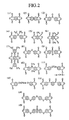
- Fig. 2 illustrates the chemical structures of fifteen dianhydrides applicable as starting material for fluorinated polyimides employed in the present invention.
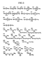
- Fig. 3 illustrates the chemical structures of thirty one diamines applicable as starting material for fluorinated polyimides employed in the present invention.
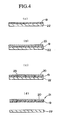
- Fig. 4 is a series of cross-sectional views showing a fabrication method for a dielectric multilayer filter in accordance with the present invention.
- Fig. 5 is a series of cross-sectional views showing another fabrication method for a dielectric multilayer filter in accordance with the present invention.
- Fig. 6 is a graph showing experimentally measured values for percent transmissiosn as a function of wavelength for a short wavelength pass filter (SWFP).
- SWFP short wavelength pass filter
- Fig. 7 is a graph showing experimentally measured values for percent transmission as a function of wavelength for a long wavelength pass filter (LWFP).
- Fig. 8 is a graph showing experimentally measured values for percent transmission as a function of wavelength for a narrow bandwidth optical filter.
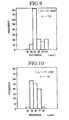
- Figs. 9 and 10 are bar graphs showing the thickness of experimentally prepared dielectric multilayer filter.
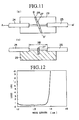
- Fig. 11(a) is a plan view of an optical element in accordance with the present invention
- Fig. 11(b) is a cross-sectional view through the line A - A′ seen in Fig. 11(a).
- Fig. 12 is a graph illustrating the spectral characteristics of the optical element shown in Figs. 11(a) and Fig. 11(b).
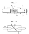
- Fig. 13 is a plan view of a second embodiment of an optical element in accordance with the present invention.
- Fig. 14 is a plan view of a third embodiment of an optical element in accordance with the present invention.
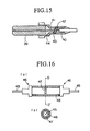
- Fig. 15 is an cross-sectional view of a fourth embodiment of an optical element in accordance with the present invention.
- Fig. 16(a) is a longitudinal cross-sectional view of a fifth embodiment of an optical element in accordance with the present invention
- Fig. 16(b) is an axial cross-sectional view through the line D - D′ seen in Fig. 16(a).
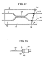
- Fig. 17 is a plan view of a sixth embodiment of an optical element in accordance with the present invention.
- Fig. 18 is an side view of a seventh embodiment of an optical element in accordance with the present invention.
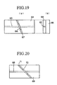
- Fig. 19(a) is a plan view of an eighth embodiment of an optical element in accordance with the present invention
- Fig. 19(b) is a side view of the optical element shown in Fig. 19(a).
- Fig. 20 is a plan view of a ninth embodiment of an optical element in accordance with the present invention.
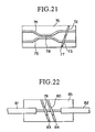
- Fig. 21 is a plan view of a tenth embodiment of an optical element in accordance with the present invention.
- Fig. 22 is a plan view of a eleventh embodiment of an optical element in accordance with the present invention.
- Fig. 23 is a plan view of a conventional optical element employing a dielectric multilayer filter
- Fig. 23(b) is a vertical cross-sectional view of the optical element shown in Fig. 23(a) through the line A - A′.
- Fig. 24 is a plan view of another conventional optical element employing a dielectric multilayer filter.
- Fig. 25 is a cross-sectional view of a conventional dielectric multilayer filter.
- Fig. 26 is a graph showing warping characteristics of two conventional dielectric multilayer filters.
- Fig. 27(a) and 27(b) are graphs showing spectral characteristics of the two conventional dielectric multilayer filters for which graphs of warping characteristics are shown in Fig. 26.
- Fig. 1 shows a cross-sectional view of a dielectric multilayer filter 21 in accordance with the present invention.
- the dielectric multilayer filter 21 consists of a fluorinated polyimide layer 19 which serves as a base layer, with an overlying dielectric multilayer 20.
- Fig. 2 illustrates the chemical structures of acid dianhydrides (1) through (15) which are applicable as a starting material for different fluorinated polyimide compounds which can be employed in the present invention.
- Fig. 3 illustrates the chemical structures of diamine compounds (1) through (31) which are applicable as a second starting material for fluorinated polyimides which can be employed in the present invention.
- one or more of the acid dianhydrides (1) through (15) shown in Fig. 2 are reacted with one or more of the diamine compounds (1) through (31) shown in Fig. 3 in a 1:1 molecular ratio in a polar organic solvent such as N-methyl pyrrolidone (NMP), N,N-dimethyl acetamide (DMAc) and the like, yielding a solution of a precursor polyamido acid.
- NMP N-methyl pyrrolidone
- DMAc N,N-dimethyl acetamide
- the compound may remain in solution, or may appear as a second phase.
- the solution may be used in later steps with no need for isolation of the fluorinated polyimide compound.
- Figs. 4(a) through 4(d) show a dielectric multilayer filter at various stages of the manufacture thereof.
- the first step involves application of fluorinated polyimide compound as a liquid over a smooth surface base plate 22 at a prescribed thickness.
- the fluorinated polyimide layer 19 is applied in this first step, in order to achieve a uniformly thin layer thereof, the layer is applied by spin coating using a solution or liquid form of the fluorinated polyimide. Having been applied, the layer is then dried and hardened, thereby yielding the solid fluorinated polyimide layer 19 over the smooth surface base plate 22 as shown in Fig. 4(a).
- Fig. 4(a) shows a dielectric multilayer filter at various stages of the manufacture thereof.
- the first step involves application of fluorinated polyimide compound as a liquid over a smooth surface base plate 22 at a prescribed thickness.
- the fluorinated polyimide layer 19 is applied in this first step, in order to achieve a uniformly thin layer thereof,
- the dielectric multilayer 20 is formed over the fluorinated polyimide layer 19 by means of an ion assist vapor deposition method.
- the layered structure is cut to a depth up to the base plate 22, resulting in the slices 23 shown in Fig. 4(c).
- the fluorinated polyimide layer 19 and dielectric multilayer 20 are together stripped away from the base plate 22 as is shown in Fig. 4(d).
- the fluorinated polyimide layer 19 and dielectric multilayer 20 may be first stripped away from the base plate 22, and then cut in to sections, rather than prior to the stripping step.
- the fluorinated polyimide layer 19 shown in Figs. 4(a) and 5(a) should have a linear thermal expansion coefficient in the range of from -0.5 x 10 ⁇ 5/C o to 10 x 10 ⁇ 5/C o .
- the majority of dielectric materials used in optical multilayers lie within this range.
- the index of refraction of such materials generally lies with in the range of from 1.5 to 1.7, depending upon the relative amount of fluorine therein.
- BK-7 glass, quartz glass, ceramic material and the like are applicable, and the greater the chemical stability and resistance to scratching thereof, the better.
- the measurements are generally carried out while the filter is still adherent to the base plate 22 as shown in Figs. 4(b) and 5(b), for which reason optically neutral properties are desirable.
- a dielectric multilayer filter was manufactured according to the method described above. Over a 30 mm diameter 0.5 mm thick BK-7 glass plate, a fluorinated polyimide layer was applied.
- the material for the layer was prepared by mixing the acid dianhydride (1) shown in Fig. 2 and the diamine (5) shown in Fig. 3 in DMAc, and reacting so as to yield a DMAc solution of the corresponding fluorinated polyamido acid. This solution was then applied to a surface of the glass plate by spin coating, after which the plate and applied layer were subjected to heating for 2 hr.
- the compound shown in structure diagram (i) had a fluorine content of 23 weight %.
- the obtained fluorinated polyimide layer had a yellow tinge, and demonstrated essentially 100% transmission over the wavelength range of from 0.4 to 1.7 ⁇ m.
- the thickness thereof was approximately 10 ⁇ m, and the refractive index was 1.61 at 1.532 ⁇ m.
- the separated filters demonstrate very slight curling at room temperature with the convexity on the side of the dielectric multilayer, the radius of curvature approximately 0.3 m. For this reason, the filters could be easily cut with scissors, and glued to a glass plate.
- the minimal curling exhibited can be explained on the basis of the fact that fluorinated polyimide compounds have a negative coefficient on the order of -0.5 x 10 ⁇ 5/C o , which is close to that of the dielectric multilayer. Because stretching forces exerted by the fluorinated polyimide layer is slightly greater than that of the dielectric multilayer both at the temperature of ion assisted vapor deposition and at ordinary temperatures, the problem of residual compression stress in the dielectric multilayer is practically eliminated. In fact, when one of this filters is placed on a 100 C o hot plate, the curling will increase somewhat, after which the the filter will revert to its original conformation upon cooling, thus mimicking the so-called bimetal effect.
- Figs. 9 and 10 which correspond to the filters for which the characteristics thereof are shown in Figs. 6 and 7, respectively.
- Figs. 9 and 10 there were two peaks in the distribution of thickness, such that filter sections having a thickness of 21 ⁇ m and 15 ⁇ m were most common. These filter sections were from the central portions of the 30 mm diameter wafers. The filter sections which were somewhat thicker than 15 ⁇ m, and those which were somewhat thicker than 21 ⁇ m were from peripheral portions. All most all of the sections had a thickness within ⁇ 2 ⁇ m of the median thickness.
- the uniformity in thickness obtained was on the same level as that for dielectric multilayer filters employing a glass base layer which required grinding and polishing to achieve a suitable thickness.
- the high consistency achieved was attributable to the fact that spin coating was used to apply the fluorinated polyimide layers. The conditions of spin coating can be adjusted so as to achieve any desired thickness for the fluorinated polyimide layer between 1 and 80 ⁇ m.
- a fluorinated polyimide material was prepared by mixing the acid dianhydride (5) shown in Fig. 2 and the diamine (13) shown in Fig. 3 in DMAc, from which dielectric multilayer filter wafers were obtained under conditions otherwise identical to those of Experimental Example 1.
- the fluorinated polyimide layer had a fluorine content of 11 weight %, a thermal expansion coefficient of 1 x 10 ⁇ 6/C o , and the structure shown in chemical structure diagram (ii) below: Curling in the filters after separation from the glass base plate was slightly more than that which occurred with the First Experimental Example, although the filters were usable.
- a fluorinated polyimide material was prepared from acid dianhydride (4) in Fig. 2 and diamine (5) in Fig. 3, from which dielectric multilayer filter wafers were obtained under conditions otherwise identical to those of Experimental Example 1.
- the fluorinated polyimide layer had a fluorine content of 31 weight %, an index of refraction of 1.5, close to that of glass, a transparent appearance, and the structure shown in chemical structure diagram (iii) below:
- the prepared filters could be easily separated from the glass base plate, but because of the large fluorine content, the dielectric multilayers readily separated from the fluorinated polyimide layer.
- the thermal expansion coefficient of the fluorinated polyimide layers was quite large at 8 x 10 ⁇ 5/C o , and was significantly different from that of the dielectric multilayers at 0.4 x 10 ⁇ 5/C o to 0.5 x 10 ⁇ 5/C o , for which reason it was thought that residual stress in the fluorinated polyimide layer of filters obtained therefrom would be significant.
- Figs. 11(a) and 11(b) show a first preferred embodiment of an optical element of the present invention.
- Fig. 11(a) is a plan view of the optical element
- Fig. 11(b) is a cross-sectional view through the line A - A′ seen in Fig. 11(a).
- An input optical fiber 24 and an output optical fiber 25 can be seen in the drawings.
- the protective coating has been removed from a portion of each fiber where the ends thereof oppose one another across a groove 28 wherein a dielectric multilayer filter 27 having a fluorinated polyimide base layer is situated.
- the above mentioned groove 28 is provided in support base 29 which additionally holds input optical fiber 24 and output optical fiber 25 in another groove provided therefor.
- an optical fiber is fixed in the groove provided in support base 29 therefor using an optical adhesive agent after aligning the optical axes thereof.
- the above mentioned groove 28 is formed in support base 29 so as to completely cut the fiber, thereby creating an input optical fiber 24 and an output optical ber 25 with mutually aligned optical axes.
- the dielectric multilayer filter 27 deviates by 8 o from a perpendicular relationship with the aligned optical axes of optical fibers 24, 25.
- the dielectric multilayer filter 27 is fixed in groove 28 using an adhesive agent suitable for optical devices.
- the dielectric multilayer filter is identical to those prepared in the First Experimental Example.
- Optical fibers 24, 25 each had a core diameter of 10 ⁇ m, cladding with an external diameter of 125 ⁇ m, and a core - cladding refractive index of 0.3%.
- losses due to diffraction of light transmitted therethrough are increased.
- the dielectric multilayer filter 27 deviates by 8 o from a perpendicular relationship with the aligned optical axes of optical fibers 24, 25, the cut off point for dielectric multilayer filter 27 is shifted slightly toward shorter wavelengths.
- Fig. 13 shows a second preferred embodiment of the optical element of the present invention.
- This optical element differs from that shown in Figs. 11(a) and 11(b) in that a plurality of optical fibers are employed in the present embodiment.
- a fiber band 30 can be seen. When viewed in cross-section, it can be appreciated that each component fiber in the fiber band 30 is separated from adjoining component fibers by a constant distance.
- a common protective layer 31 surrounds all of the component optical fibers.
- dielectric multilayer filter 32 which incorporates a fluorinated polyimide base layer.
- a groove 33 is provided in a support base 34 for mounting the above mentioned dielectric multilayer filter 32.
- a dielectric multilayer filter 32 identical to that used in the first preferred embodiment can be suitably employed.
- Fig. 14 shows an optical element in accordance with a third preferred embodiment of the optical element of the present invention, which is applicable to devices acting as a polarizer.
- a polarization maintaining optical fiber 35 a dielectric multilayer filter 36 with a fluorinated polyimide base layer, groove 37, and base support 38 can be seen.
- the groove 37 wherein the dielectric multilayer filter 36 is vertically mounted on base support 38 forms an angle of 45 o with the optical axis of the optical element so as to enhance the polarization effect in dielectric multilayer filter 36.
- the plane of polarization of maintaining optical fiber 35 is aligned so as to be oriented at an angle of either 0 o or 90 o with respect to base support 38.
- Fig. 15 shows an optical element in accordance with a fourth preferred embodiment of the optical element of the present invention.
- a ferrule formed by zirconia ceramic male portion 39 and stainless steel female portion 40, an optical fiber 41, a filter 42 with a fluorinated polyimide base layer, groove 43 wherein filter 42 is mounted, and optical adhesive agent 44 can be seen.
- the above described ferrule structure makes this optical element to optical fiber connectors and the like. Additionally, the ferrule makes it possible to connect this optical element with various other types of fiber optic equipment.
- Fig. 16 shows an optical element in accordance with a fifth preferred embodiment of the optical element of the present invention.
- an optical fiber 45 a ferrule 46 for receiving the end of optical fiber 45, and a filter 47 with a fluorinated polyimide base layer can be seen.
- a sleeve 48 fits over ferrule 46, whereby the position of the end point of optical fiber 45 can be adjusted with precision.
- the end surface of ferrule 46 within sleeve 48 can be perpendicular to the optical axis of optical fiber 45, or can be at an angle therewith, or have a spherical shape.
- the configuration of the p resent embodiment facilitates connecting an optical fiber device with various other types of devices with a predetermined accurate and reliable alignment.
- Fig. 17 shows an optical element in accordance with a sixth preferred embodiment of the optical element of the present invention.
- the illustrated device is a type of multiple pathway optically coupling-splitting device, or a commonly referred to, an optical fiber coupler, in which two dielectric multilayer filters are incorporated.
- an optical fiber coupler in which two dielectric multilayer filters are incorporated.
- two or more optical fibers are brought into close approximation with one another in a parallel arrangement over a portion of their lengths to form an optical coupling region, whereby wavelength dependent optical coupling is achieved.
- the optical element of Fig. 17 includes two input optical fibers 49, 50, two output optical fibers 51, 52, an optical coupling region 53, two dielectric multilayer filter leaves 54, 55, each having a fluorinated polyimide base layer, a groove 56 wherein dielectric multilayer filter leaves 54 and 55 are mounted, and a base support 56 whereby input optical fibers 49 and 50, output optical fibers 51 and 52 and dielectric multilayer filter leaves 54 and 55 are supported.
- the optical element of Fig. 17 offers significant improvements in wavelength selectivity over conventional optical fiber couplers, based on the previously described features which are inherent to the dielectric multilayer filter of the present invention.
- optical element has applications in which the optical fibers 51, 52 are the input optical fibers and optical fibers 49, 50 are the output optical fibers, that is to say, input optical signals traverse the dielectric multilayer filters 54, 55 prior to entering the coupling region 53.
- undesirable wavelength components can be effectively eliminated before splitting of other wavelength components takes place in the coupling region 53.
- Fig. 18 shows an optical element in accordance with a seventh preferred embodiment of the optical element of the present invention.
- an input optical fiber 58 and optical receiver 59 can be seen, with a dielectric multilayer filter 60 with a fluorinated polyimide base layer intervening therebetween.
- the optical receiver 59 is provided with a glass window 61 and a semiconductor optical receiver cell 62. Because no mechanical coupling fittings are included, it is necessary to carefully align the optical axis of optical fiber 58 with that of optical receiver 59.
- Fig. 19 shows an optical element in accordance with a eighth preferred embodiment of the optical element of the present invention, in which a dielectric multilayer filter 66 with a fluorinated polyimide base layer is incorporated into a glass optical waveguide.
- the illustrated device includes an optical waveguide consisting of a core 63 and cladding 64, base plate 65 from which the optical waveguide is formed, and a groove 67 in which the above mentioned dielectric multilayer filter 66 is mounted.
- multiple optical waveguides can be provided in parallel leading up to the single dielectric multilayer filter 66.
- a pig tail type filter can be fabricated for joining optical fibers to an optical waveguide.
- Fig. 20 shows an optical element in accordance with a ninth preferred embodiment of the optical element of the present invention, which is applicable to devices acting as a polarizer.
- a dielectric multilayer filter 70 with a fluorinated polyimide base layer is included, mounted at an angle of approximately 45 o with respect to the optical axis of an optical waveguide core 68.
- the dielectric multilayer filter 70 is mounted in a groove 71 in a supporting base (not shown).
- the principal axis of the optical waveguide is inherently mounted on the supporting base such that either polarization parallel to the supporting base (TE polarization) or polarization perpendicular to the supporting base (TM polarizaiton) can be supported. Accordingly, in contrast to the optical element of the third embodiment, with the optical element of the present embodiment, the necessity for rotationally aligning axes of polarization is eliminated.
- Fig. 21 shows an optical element in accordance with a tenth preferred embodiment of the optical element of the present invention.
- the illustrated device is a type of optical coupler device in which two dielectric multilayer filters 72, 73 with fluorinated polyimide base layers are incorporated into either the input pathway or output pathway thereof.
- the optical element shown in Fig. 21 includes the above mentioned two dielectric multilayer filters 72, 73 with fluorinated polyimide base layers, two cores 74, 75 and cladding 76 of the optical waveguide, a groove 77 wherein dielectric multilayer filter leaves 54 and 55 are mounted, and an optical coupling region 78.
- the function of this device is essentially identical to that of the sixth preferred embodiment.
- Fig. 22 shows an optical element in accordance with an eleventh preferred embodiment of the optical element of the present invention which incorporates multiple dielectric multilayer filters with fluorinated polyimide base layers.
- the optical element shown in Fig. 22 includes two dielectric multilayer filters 79, 80 with fluorinated polyimide base layers, two optical fibers 81, 82, two grooves 83, 84 for dielectric multilayer filters 79, 80, respectively, and a supporting base 85.
- This device makes it possible to eliminate two or more undesirable wavelength components from an input optical signal, and is especially useful when the wavelengths of the components to be removed cannot be practically filtered out with a single filter.
- multiple dielectric multilayer filters with fluorinated polyimide base layers can be inserted into a single optical pathway in any of the preceding ten embodiments.
Landscapes
- Physics & Mathematics (AREA)
- General Physics & Mathematics (AREA)
- Optics & Photonics (AREA)
- Engineering & Computer Science (AREA)
- Microelectronics & Electronic Packaging (AREA)
- Optical Filters (AREA)
Applications Claiming Priority (2)
| Application Number | Priority Date | Filing Date | Title |
|---|---|---|---|
| JP31766/90 | 1990-02-13 | ||
| JP3176690 | 1990-02-13 |
Publications (3)
| Publication Number | Publication Date |
|---|---|
| EP0442801A2 true EP0442801A2 (fr) | 1991-08-21 |
| EP0442801A3 EP0442801A3 (en) | 1991-12-04 |
| EP0442801B1 EP0442801B1 (fr) | 1995-05-10 |
Family
ID=12340166
Family Applications (1)
| Application Number | Title | Priority Date | Filing Date |
|---|---|---|---|
| EP91400346A Expired - Lifetime EP0442801B1 (fr) | 1990-02-13 | 1991-02-12 | Procédé de fabrication d'un filtre diélectrique à couches multiples |
Country Status (3)
| Country | Link |
|---|---|
| US (2) | US5234772A (fr) |
| EP (1) | EP0442801B1 (fr) |
| DE (1) | DE69109513T2 (fr) |
Cited By (5)
| Publication number | Priority date | Publication date | Assignee | Title |
|---|---|---|---|---|
| GB2301249A (en) * | 1995-05-24 | 1996-11-27 | Bosch Gmbh Robert | Optical transceiver |
| DE4124937C2 (de) * | 1990-09-21 | 1999-08-26 | O I B Gmbh Optische Interferen | Verfahren zur Herstellung eines optischen Interferenzschichtsystems |
| EP1078896A1 (fr) * | 1999-08-10 | 2001-02-28 | Kabushiki Kaisha Ohara | Vitrocerame pour un filtre optique et ce filtre optique |
| EP0957379A3 (fr) * | 1998-05-12 | 2003-01-15 | SEIKOH GIKEN Co., Ltd. | Filtre à longueur d'onde fibre optique et procédé pour sa fabrication |
| US6677259B2 (en) | 1999-08-10 | 2004-01-13 | Kabushiki Kaisha Ohara | Glass-ceramics for a light filter |
Families Citing this family (19)
| Publication number | Priority date | Publication date | Assignee | Title |
|---|---|---|---|---|
| JPH06201936A (ja) * | 1992-12-28 | 1994-07-22 | Matsushita Electric Ind Co Ltd | 光ファイバアレイ及びその製造方法 |
| KR100310092B1 (ko) * | 1998-11-18 | 2001-11-07 | 윤종용 | 광통신용 폴리이미드, 그 제조방법 및 그것을 이용한 다층 폴리이미드막의 형성방법 |
| US6678087B1 (en) * | 1999-08-06 | 2004-01-13 | Nippon Telegraph And Telephone Corporation | Optical amplifier and optical fiber communication system using the amplifier |
| ATE478913T1 (de) | 2000-06-02 | 2010-09-15 | Stanford Res Inst Int | Polymermembranzusammensetzung |
| US6842564B2 (en) | 2001-04-05 | 2005-01-11 | Richard H. Laughlin | Remotely configurable add/drop for wavelength division multiplexing and method of operating the same |
| US7316855B2 (en) | 2001-06-01 | 2008-01-08 | Polyfuel, Inc. | Fuel cell assembly for portable electronic device and interface, control, and regulator circuit for fuel cell powered electronic device |
| WO2002099916A2 (fr) | 2001-06-01 | 2002-12-12 | Polyfuel, Inc | Ensemble pile a combustible destine a un dispositif electronique portable et circuit d'interface, de commande et de regulation pour dispositif electronique alimente par pile a combustible |
| JP4199442B2 (ja) * | 2001-07-25 | 2008-12-17 | 富士通株式会社 | 波長特性可変装置 |
| TW200634099A (en) * | 2004-12-08 | 2006-10-01 | Clariant Int Ltd | Pyridine n-oxide based azo dyes and their metal complexes for use in optical layers for optical data recording |
| JP2006189596A (ja) * | 2005-01-06 | 2006-07-20 | Central Glass Co Ltd | 光学多層膜フィルタの製造方法及び光学多層膜フィルタ |
| JP2006215212A (ja) * | 2005-02-02 | 2006-08-17 | Omron Corp | 光合分波器とその製造方法 |
| TW200730906A (en) * | 2005-11-18 | 2007-08-16 | Hitachi Chemical Co Ltd | Optical device |
| US7275532B2 (en) * | 2005-11-28 | 2007-10-02 | Niemackl Douglas J | Bow blind |
| JP2007201670A (ja) * | 2006-01-25 | 2007-08-09 | Hitachi Communication Technologies Ltd | 光伝送システム |
| CN102067483A (zh) * | 2008-04-21 | 2011-05-18 | 奥普林克通信公司 | 光纤网络监控 |
| JP6742593B2 (ja) * | 2015-01-05 | 2020-08-19 | 日本電気硝子株式会社 | 支持ガラス基板の製造方法及び積層体の製造方法 |
| JP6601982B2 (ja) | 2015-10-22 | 2019-11-06 | 日本碍子株式会社 | 光導波路基板の製造方法 |
| KR102759519B1 (ko) * | 2017-07-19 | 2025-01-23 | 도판 홀딩스 가부시키가이샤 | 파장 변환 시트 및 그 제조 방법 |
| KR20230070168A (ko) * | 2020-09-24 | 2023-05-22 | 가부시키가이샤 크리에이티브 테크놀러지 | 집진기 및 집진 방법 |
Family Cites Families (9)
| Publication number | Priority date | Publication date | Assignee | Title |
|---|---|---|---|---|
| US4212457A (en) * | 1978-03-27 | 1980-07-15 | Xerox Corporation | Pre/post-collation copying system |
| US4674866A (en) * | 1983-09-16 | 1987-06-23 | Canon Kabushiki Kaisha | Method and apparatus for two-side image formation |
| GB2189621B (en) * | 1986-03-06 | 1989-11-08 | Nippon Sheet Glass Co Ltd | Optical demultiplexer and/or multiplexer |
| US4714241A (en) * | 1986-08-04 | 1987-12-22 | Eastman Kodak Company | Recirculating document feeder |
| JPS6364003A (ja) * | 1986-09-05 | 1988-03-22 | Teijin Ltd | 光学フイルタ− |
| US4952666A (en) * | 1988-05-06 | 1990-08-28 | Hughes Aircraft Company | Hexafluoroisopropylidene-containing polyimide oligomers and polymers |
| US4954578A (en) * | 1988-10-25 | 1990-09-04 | International Business Machines Corporation | Fine domain composite films of polyimide mixtures |
| US4933132A (en) * | 1989-02-28 | 1990-06-12 | Hoechst Celanese Corp. | Process of making a shaped article from intermediate molecular weight polyimides |
| CA2041133C (fr) * | 1990-04-27 | 1995-01-03 | Toru Matsuura | Guide de lumiere a polyimide |
-
1991
- 1991-02-12 EP EP91400346A patent/EP0442801B1/fr not_active Expired - Lifetime
- 1991-02-12 DE DE69109513T patent/DE69109513T2/de not_active Expired - Lifetime
- 1991-02-12 US US07/654,010 patent/US5234772A/en not_active Expired - Lifetime
-
1993
- 1993-04-30 US US08/054,319 patent/US5332535A/en not_active Expired - Lifetime
Cited By (7)
| Publication number | Priority date | Publication date | Assignee | Title |
|---|---|---|---|---|
| DE4124937C2 (de) * | 1990-09-21 | 1999-08-26 | O I B Gmbh Optische Interferen | Verfahren zur Herstellung eines optischen Interferenzschichtsystems |
| GB2301249A (en) * | 1995-05-24 | 1996-11-27 | Bosch Gmbh Robert | Optical transceiver |
| EP0957379A3 (fr) * | 1998-05-12 | 2003-01-15 | SEIKOH GIKEN Co., Ltd. | Filtre à longueur d'onde fibre optique et procédé pour sa fabrication |
| EP1078896A1 (fr) * | 1999-08-10 | 2001-02-28 | Kabushiki Kaisha Ohara | Vitrocerame pour un filtre optique et ce filtre optique |
| US6410466B1 (en) | 1999-08-10 | 2002-06-25 | Kabushiki Kaisha Ohara | Glass-ceramics for a light filter |
| EP1219574A1 (fr) * | 1999-08-10 | 2002-07-03 | Kabushiki Kaisha Ohara | Vitrocerame pour un filtre optique et ce filtre optique |
| US6677259B2 (en) | 1999-08-10 | 2004-01-13 | Kabushiki Kaisha Ohara | Glass-ceramics for a light filter |
Also Published As
| Publication number | Publication date |
|---|---|
| EP0442801B1 (fr) | 1995-05-10 |
| US5332535A (en) | 1994-07-26 |
| US5234772A (en) | 1993-08-10 |
| DE69109513T2 (de) | 1996-01-18 |
| EP0442801A3 (en) | 1991-12-04 |
| DE69109513D1 (de) | 1995-06-14 |
Similar Documents
| Publication | Publication Date | Title |
|---|---|---|
| EP0442801B1 (fr) | Procédé de fabrication d'un filtre diélectrique à couches multiples | |
| US4431260A (en) | Method of fabrication of fiber optic coupler | |
| EP0124523B1 (fr) | Commutateur pour fibres optiques et ligne a retard a variation discrete | |
| US6879752B1 (en) | Film spacer for setting the gap between an optical coupler and a whispering-gallery mode optical resonator | |
| CA2245409C (fr) | Guide d'ondes optiques plan | |
| CA1248384A (fr) | Ligne a retard continument variable a fibre optique | |
| EP0701150B1 (fr) | Méthode de production de réflecteurs de Bragg pour guides d'ondes et produits obtenus | |
| WO2004001463A1 (fr) | Guide d'ondes optiques | |
| US20030031446A1 (en) | Freestanding athermal polymer optical waveguide | |
| JP2608633B2 (ja) | 誘電体多層膜フィルタおよびその製造方法並びにこれを用いた光学要素 | |
| CA2438185C (fr) | Procede et appareil pour filtre optique | |
| US4452505A (en) | Bidirectional coupler for communication over a single fiber | |
| US6477308B2 (en) | Optical waveguide devices and methods of fabricating the same | |
| Lukosz et al. | Determination of thickness, refractive indices, optical anisotropy of, and stresses in SiO2 films on silicon wafers | |
| US20030175007A1 (en) | Optical filter array and method of use | |
| KR20030004124A (ko) | 광도파로 | |
| KR20000036055A (ko) | 광학 소자를 제조하는 방법 및 이 방법에 따라 제조된 광학 소자 | |
| US4961801A (en) | Method of making a bidirectional coupler for communication over single fiber | |
| GB2072876A (en) | Bidirectional coupler for communication over a single fibre | |
| DE4433738A1 (de) | Doppelbrechungsarmer planarer optischer Wellenleiter und Verfahren zu seiner Herstellung | |
| KR100351562B1 (ko) | 역다중화기 | |
| EP1327170A2 (fr) | Utilisation de gaz source a base de deuterium afin de fabriquer des guides d'ondes a faible perte en gesion-sion | |
| JP2003149479A (ja) | 石英系ガラス光導波路及びそれを用いた光モジュール | |
| JPS6360410A (ja) | 光デバイスの製造方法 | |
| Subias et al. | Wavelength selective optical fiber couplers based on longitudinal Fabry-Perot structures |
Legal Events
| Date | Code | Title | Description |
|---|---|---|---|
| PUAI | Public reference made under article 153(3) epc to a published international application that has entered the european phase |
Free format text: ORIGINAL CODE: 0009012 |
|
| AK | Designated contracting states |
Kind code of ref document: A2 Designated state(s): DE FR GB |
|
| PUAL | Search report despatched |
Free format text: ORIGINAL CODE: 0009013 |
|
| 17P | Request for examination filed |
Effective date: 19910928 |
|
| AK | Designated contracting states |
Kind code of ref document: A3 Designated state(s): DE FR GB |
|
| 17Q | First examination report despatched |
Effective date: 19931022 |
|
| GRAA | (expected) grant |
Free format text: ORIGINAL CODE: 0009210 |
|
| AK | Designated contracting states |
Kind code of ref document: B1 Designated state(s): DE FR GB |
|
| REF | Corresponds to: |
Ref document number: 69109513 Country of ref document: DE Date of ref document: 19950614 |
|
| ET | Fr: translation filed | ||
| PLBE | No opposition filed within time limit |
Free format text: ORIGINAL CODE: 0009261 |
|
| STAA | Information on the status of an ep patent application or granted ep patent |
Free format text: STATUS: NO OPPOSITION FILED WITHIN TIME LIMIT |
|
| 26N | No opposition filed | ||
| REG | Reference to a national code |
Ref country code: FR Ref legal event code: CA |
|
| REG | Reference to a national code |
Ref country code: GB Ref legal event code: IF02 |
|
| PGFP | Annual fee paid to national office [announced via postgrant information from national office to epo] |
Ref country code: FR Payment date: 20100223 Year of fee payment: 20 |
|
| PGFP | Annual fee paid to national office [announced via postgrant information from national office to epo] |
Ref country code: DE Payment date: 20100219 Year of fee payment: 20 Ref country code: GB Payment date: 20100202 Year of fee payment: 20 |
|
| REG | Reference to a national code |
Ref country code: DE Ref legal event code: R071 Ref document number: 69109513 Country of ref document: DE |
|
| REG | Reference to a national code |
Ref country code: GB Ref legal event code: PE20 Expiry date: 20110211 |
|
| PG25 | Lapsed in a contracting state [announced via postgrant information from national office to epo] |
Ref country code: GB Free format text: LAPSE BECAUSE OF EXPIRATION OF PROTECTION Effective date: 20110211 |
|
| PG25 | Lapsed in a contracting state [announced via postgrant information from national office to epo] |
Ref country code: DE Free format text: LAPSE BECAUSE OF EXPIRATION OF PROTECTION Effective date: 20110212 |