EP0440139B1 - Heisse-Elektronen-Transistor - Google Patents
Heisse-Elektronen-Transistor Download PDFInfo
- Publication number
- EP0440139B1 EP0440139B1 EP91101080A EP91101080A EP0440139B1 EP 0440139 B1 EP0440139 B1 EP 0440139B1 EP 91101080 A EP91101080 A EP 91101080A EP 91101080 A EP91101080 A EP 91101080A EP 0440139 B1 EP0440139 B1 EP 0440139B1
- Authority
- EP
- European Patent Office
- Prior art keywords
- barrier layer
- collector
- layer
- emitter
- base
- Prior art date
- Legal status (The legal status is an assumption and is not a legal conclusion. Google has not performed a legal analysis and makes no representation as to the accuracy of the status listed.)
- Expired - Lifetime
Links
Images

Classifications
-
- H—ELECTRICITY
- H10—SEMICONDUCTOR DEVICES; ELECTRIC SOLID-STATE DEVICES NOT OTHERWISE PROVIDED FOR
- H10D—INORGANIC ELECTRIC SEMICONDUCTOR DEVICES
- H10D48/00—Individual devices not covered by groups H10D1/00 - H10D44/00
- H10D48/01—Manufacture or treatment
- H10D48/031—Manufacture or treatment of three-or-more electrode devices
- H10D48/032—Manufacture or treatment of three-or-more electrode devices of unipolar transistors having ohmic electrodes on emitter-like, base-like, and collector-like regions, e.g. hot electron transistors [HET], metal base transistors [MBT], resonant tunneling transistors [RTT], bulk barrier transistors [BBT], planar doped barrier transistors [PDBT] or charge injection transistors [CHINT]
-
- H—ELECTRICITY
- H10—SEMICONDUCTOR DEVICES; ELECTRIC SOLID-STATE DEVICES NOT OTHERWISE PROVIDED FOR
- H10D—INORGANIC ELECTRIC SEMICONDUCTOR DEVICES
- H10D48/00—Individual devices not covered by groups H10D1/00 - H10D44/00
- H10D48/30—Devices controlled by electric currents or voltages
- H10D48/32—Devices controlled by only the electric current supplied, or only the electric potential applied, to an electrode which does not carry the current to be rectified, amplified or switched
- H10D48/36—Unipolar devices
- H10D48/362—Unipolar transistors having ohmic electrodes on emitter-like, base-like, and collector-like regions, e.g. hot electron transistors [HET], metal base transistors [MBT], resonant tunnelling transistors [RTT], bulk barrier transistors [BBT], planar doped barrier transistors [PDBT] or charge injection transistors [CHINT]
Definitions
- the present invention relates to a semiconductor device, and more particularly to a hot electron transistor (HET).
- HET hot electron transistor
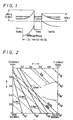
- An HET operable in a room temperature is disclosed in, for example, Applied Physics Letters Vol. 51, No. 13, pp 984 - 986, September 1987, which is constituted by disposing an emitter barrier layer 2 made of AlSb 0.92 As 0.08 and a collector barrier layer 3 made of GaAs at opposite sides of a base layer 1 made of InAs respectively so as to sandwich the base layer 1 therebetween, as shown in Fig. 1 which is a band model diagram of its conduction band in a biasing state.
- an offset gap ⁇ E B-C of a conduction band between the base and the collector of the HET thus constructed is 0.8 eV
- an offset gap ⁇ E B-E of a conduction band of the emitter barrier layer between the base and the emitter is to be selected larger than the offset gap ⁇ E B-C .
- the offset gap ⁇ E B-E of 1.3 ev is established for the HET.
- the gap ⁇ E B-E between the base and the emitter being such a high value of 1.3 ev, an energy of a hot electron injected from the emitter into the collector is too high to neglect the ionization in the collector due to the hot electron.
- the hot electrons of high energy injected in the collector eject electrons from a valence band in the collector to generate an avalanche current, which degrades the saturation characteristics of the transistor.
- Hatched portions in Fig. 1 show an energy level where electrons exist.
- a layer adjacent to the base layer 1 of In-system, that is, the emitter barrier layer 2 is made of Al-system, which causes a difficulty in setting a selection ratio of etching between the layers of the Al-system and the In-system. Accordingly, upon leading a base electrode from the base layer 1 of the In-system which forms this kind of HET in actual practice, there arises a problem that an etching process for partially removing the In-system emitter barrier layer or emitter layer on the base layer 1 in order to partially expose the base layer 1 is extremely difficult.
- an object of the present invention to provide an HET having an InAs base layer which is capable of improving the saturation characteristics and symplifying the fabrication process thereof.
- a hot electron transistor is comprised of an InAs base layer, a GaSb emitter barrier layer deposited on one side of the InAs base layer, and a GaInAsSb collector barrier layer deposited on the other side of said InAs layer, whereby the InAs base layer is sandwiched between the GaSb emitter barrier layer and the GaInAsSb collector barrier layer the offset gap ⁇ E B-C of the conduction band between the base and the collector being selected more than 0.4 eV but less than 0.8 eV.
- Fig. 2 is a graph showing the relationship among the composition, the band gap and the lattice constant of Ga x In 1-x As y Sb 1-y shown on page 41 of "HETERO-STRUCTURE LASERS", Part B, by H. C. Casey, and Jr M. B. Panish, published by Academic Press.
- the GaInAsSb-system semiconductor has a band gap smaller than 0.8 eV.
- HET hot electron transistor
- an n-type GaSb collector layer 10 having a thickness of 200 nm, an intrinsic GaSb underlaying layer 13A having a thickness of 100 nm for a collector barrier layer, an intrinsic Ga x In 1-x As y Sb 1-y , for example, Ga 0.8 In 0.2 As 0.2 Sb 0.8 collector barrier layer 13 having a thickness of 10 nm, an n-type InAs base layer 11 having a thickness of 10 nm, an intrinsic GaAs emitter barrier layer 12 having a thickness of 100 nm, and an n-type highly concentration GaSb emitter layer 14 having a thickness of 200 nm.
- the emitter layer 14 and the emitter barrier layer 12 are partially etched away by an etching method which has selectively in stching Ga-system and In-system materials, for example, a reactive ion etching (RIE) method using a CCl2F2+He system to thereby partially expose a part of the base layer 11.
- RIE reactive ion etching
- a base electrode 15 is made in ohmic contact with the exposed surface of the base layer 11, and simultaneously an emitter electrode 16 is deposited on the emitter layer 14 in an ohmic contact therewith.
- a collector electrode 17 is ohmicly deposited, for example, on the rear surface of the substrate 9.
- the offset gap ⁇ E B-E of the conduction band between the base and the emitter becomes 0.8 ev, while the offset gap ⁇ E B-C between the base and the collector falls in a range of more than 0.4 - and less than 0.8 eV, thereby making it possible for this device to operate as a transistor at room temperature.
- the lattice constants thereof match or favorably match with the lattice constants of InAs constituting the base layer 11 to thereby make it possible to perform a good epitaxy. Further, it is possible to perform a good epitaxy of the GaSb emitter barrier layer 12 on this InAs base layer 11.
- the offset gap ⁇ E B-C between the base and the collector can be fallen within a range of 0.4 eV - 0.8 eV while the offset gap ⁇ E B-E between the base and the emitter can be determined as 0.8 eV.
- the respective layers 10-13A-13-11-12-14 can be formed continuously and epitaxially as a series of works by the MOCVD (Metal Organic Chemical Vapor Deposition) method, MBE (molecular Beam Epitaxy) method and so on.
- MOCVD Metal Organic Chemical Vapor Deposition
- MBE molecular Beam Epitaxy
- Reference numerals 18 and 19 in Fig. 3 respectively designate insulating layers, each made of, for example, oxide materials or the like.
- GaSb substrate 9 is used in the embodiment shown in Fig. 3, in some cases GaSb or InAs substrate of, for example, n-type having a high impurity concentration, i.e. low resistivity may be provided, and thereon the GaSb collector layer 10 may be epitaxially grown. Also in this case, the respective layers on the substrate 9 can be epitaxially grown successively by a series of works by the MOCVD method or the MBE method.
- the offset gap ⁇ E B-C of the conduction band between the base and the collector can be made smaller than 0.8 eV.
- the offset gap ⁇ E B-E of the conduction band between the base and the emitter of the emitter barrier layer 12 can be made such a relatively small value of 0.8 eV.
- the selective etching for the emitter layer 14 and the emitter barrier layer 12 in order to partially expose the base layer 11 is performed by using the CCl2F2+He-system etching gas which has different etching speeds between the Ga-system material and In-system material, so that one portion of the base layer 11 can be exposed outside easily.
Landscapes
- Bipolar Transistors (AREA)
Claims (5)
- Heißelektronen-Transistor, bestehend aus:
einer InAs-Basisschicht (11),
einer auf einer Seite der InAs-Basisschicht (11) aufgebrachten GaSb-Emittersperrschicht (12) und
einer auf der anderen Seite der InAs-Basisschicht (11) aufgebrachten Kollektorsperrschicht (13), wobei die InAs-Basisschicht (11) zwischen der GaSb-Emittersperrschicht (12) und der Kollektorsperrschicht (13) angeordnet ist,
dadurch gekennzeichnet,
daß die Kollektorsperrschicht (13) aus GaInAsSb gebildet ist, wobei die Versatzlücke ΔEB-C des Leitungsbandes zwischen der Basis und dem Kollektor größer als 0,4 eV aber kleiner als 0,8 eV gewählt ist. - Heißelektronen-Transistor nach Anspruch 1, mit einem GaSb-Substrat (9, 10), auf welchem die Kollektorsperrschicht (13), die Basisschicht (11) und die Emittersperrschicht (12) in Folge epitaktisch abgeschieden sind.
- Heißelektronen-Transistor nach Anspruch 1 oder 2, wobei die Basisschicht (11) n-leitend, die Emittersperrschicht (12) eigenleitend und die Kollektorsperrschicht (13) eigenleitend ist.
- Verfahren zur Herstellung eines Heißelektronen-Transistors nach einem der Ansprüche 1 bis 3, wobei die Basisschicht (11), die Emittersperrschicht (12) und die Kollektorsperrschicht (13) durch ein metallorganisches chemisches Dampfabscheidungsverfahren (MOCVD-Verfahren) gebildet werden.
- Verfahren zur Herstellung eines Heißelektronen-Transistors nach einem der Ansprüche 1 bis 3, wobei die Basisschicht (11), die Emittersperrschicht (12) und die Kollektorsperrschicht (13) durch ein Molekularstrahl-Epitaxie-Verfahren (MBE-Verfahren) gebildet werden.
Applications Claiming Priority (2)
| Application Number | Priority Date | Filing Date | Title |
|---|---|---|---|
| JP18707/90 | 1990-01-29 | ||
| JP2018707A JP2527060B2 (ja) | 1990-01-29 | 1990-01-29 | 半導体装置 |
Publications (2)
| Publication Number | Publication Date |
|---|---|
| EP0440139A1 EP0440139A1 (de) | 1991-08-07 |
| EP0440139B1 true EP0440139B1 (de) | 1994-12-14 |
Family
ID=11979123
Family Applications (1)
| Application Number | Title | Priority Date | Filing Date |
|---|---|---|---|
| EP91101080A Expired - Lifetime EP0440139B1 (de) | 1990-01-29 | 1991-01-28 | Heisse-Elektronen-Transistor |
Country Status (4)
| Country | Link |
|---|---|
| US (1) | US5124771A (de) |
| EP (1) | EP0440139B1 (de) |
| JP (1) | JP2527060B2 (de) |
| DE (1) | DE69105762T2 (de) |
Families Citing this family (8)
| Publication number | Priority date | Publication date | Assignee | Title |
|---|---|---|---|---|
| US5326985A (en) * | 1992-09-28 | 1994-07-05 | Motorola, Inc. | Bipolar doped semiconductor structure and method for making |
| US5298763A (en) * | 1992-11-02 | 1994-03-29 | Motorola, Inc. | Intrinsically doped semiconductor structure and method for making |
| US5436469A (en) * | 1994-06-15 | 1995-07-25 | Moll; Nicolas J. | Band minima transistor |
| KR0170474B1 (ko) * | 1995-12-21 | 1999-02-01 | 정선종 | 공진 터널링 핫전자 장치 |
| JP3388090B2 (ja) * | 1996-04-26 | 2003-03-17 | 富士通株式会社 | 電流駆動される半導体装置および高移動度トランジスタ |
| KR19980034078A (ko) * | 1996-11-05 | 1998-08-05 | 양승택 | 핫 전자 장치(Hot Electron Device) 및 공진 터널링 핫 전자 장치 |
| WO2005074042A1 (en) * | 2004-01-22 | 2005-08-11 | Hall, Robert, B. | Phototransistors, methods of making phototransistors, and methods of detecting light |
| US7639459B2 (en) * | 2005-01-10 | 2009-12-29 | Hitachi Global Storage Technologies Netherlands B.V. | Three terminal magnetic sensor having an in-stack longitudinal biasing layer structure |
Citations (1)
| Publication number | Priority date | Publication date | Assignee | Title |
|---|---|---|---|---|
| EP0159273A2 (de) * | 1984-04-17 | 1985-10-23 | Fujitsu Limited | Halbleiteranordnung |
Family Cites Families (2)
| Publication number | Priority date | Publication date | Assignee | Title |
|---|---|---|---|---|
| JPS63229752A (ja) * | 1987-03-19 | 1988-09-26 | Fujitsu Ltd | 超高速半導体装置 |
| US4829343A (en) * | 1987-07-17 | 1989-05-09 | American Telephone & Telegraph Company, At&T Bell Laboratories | Hot electron transistor |
-
1990
- 1990-01-29 JP JP2018707A patent/JP2527060B2/ja not_active Expired - Fee Related
-
1991
- 1991-01-28 EP EP91101080A patent/EP0440139B1/de not_active Expired - Lifetime
- 1991-01-28 DE DE69105762T patent/DE69105762T2/de not_active Expired - Fee Related
- 1991-01-29 US US07/647,411 patent/US5124771A/en not_active Expired - Fee Related
Patent Citations (1)
| Publication number | Priority date | Publication date | Assignee | Title |
|---|---|---|---|---|
| EP0159273A2 (de) * | 1984-04-17 | 1985-10-23 | Fujitsu Limited | Halbleiteranordnung |
Also Published As
| Publication number | Publication date |
|---|---|
| DE69105762T2 (de) | 1995-04-27 |
| EP0440139A1 (de) | 1991-08-07 |
| US5124771A (en) | 1992-06-23 |
| JPH03222478A (ja) | 1991-10-01 |
| JP2527060B2 (ja) | 1996-08-21 |
| DE69105762D1 (de) | 1995-01-26 |
Similar Documents
| Publication | Publication Date | Title |
|---|---|---|
| Dumke et al. | GaAs GaAlAs heterojunction transistor for high frequency operation | |
| US5001534A (en) | Heterojunction bipolar transistor | |
| US4665412A (en) | Coupled heterostructure superlattice devices | |
| JP2801624B2 (ja) | ヘテロ接合バイポーラトランジスタ | |
| EP0619613B1 (de) | Heteroübergang-Bipolartransistor | |
| EP0255288A2 (de) | Resonanter Tunneltransistor | |
| EP0507454B1 (de) | Halbleiteranordnung mit einem Heteroübergang-Bipolartransistor und Verfahren zu seiner Herstellung | |
| EP0199435B1 (de) | Feldeffekt-Halbleiteranordnung | |
| JPH0750410A (ja) | 半導体結晶積層体及びその形成方法並びに半導体装置 | |
| US20020190273A1 (en) | Bipolar transistor with upper heterojunction collector and method for making same | |
| EP0306258A2 (de) | Transistor | |
| EP0440139B1 (de) | Heisse-Elektronen-Transistor | |
| JPH07118531B2 (ja) | ホットエレクトロン・ユニポーラ・トランジスタ | |
| US5106766A (en) | Method of making a semiconductor device that comprises p-type III-V semiconductor material | |
| EP0566591A1 (de) | Halbleitervorrichtung. | |
| US4929984A (en) | Resonant tunnelling barrier structure device | |
| US5206524A (en) | Heterostructure bipolar transistor | |
| EP0331482B1 (de) | Transistorstruktur | |
| US5912480A (en) | Heterojunction semiconductor device | |
| JP2687519B2 (ja) | 半導体装置及びその製造方法 | |
| EP0229672B1 (de) | Bipolarer Heteroübergangstransistor mit einem Basisbereich aus Germanium | |
| JPH032350B2 (de) | ||
| JPH0337735B2 (de) | ||
| EP0361759A2 (de) | Heterostrukturbipolartransistor | |
| EP0697741A1 (de) | Anordnungen mit resonantem Tunneleffekt |
Legal Events
| Date | Code | Title | Description |
|---|---|---|---|
| PUAI | Public reference made under article 153(3) epc to a published international application that has entered the european phase |
Free format text: ORIGINAL CODE: 0009012 |
|
| AK | Designated contracting states |
Kind code of ref document: A1 Designated state(s): DE FR GB |
|
| 17P | Request for examination filed |
Effective date: 19920206 |
|
| 17Q | First examination report despatched |
Effective date: 19930510 |
|
| GRAA | (expected) grant |
Free format text: ORIGINAL CODE: 0009210 |
|
| AK | Designated contracting states |
Kind code of ref document: B1 Designated state(s): DE FR GB |
|
| REF | Corresponds to: |
Ref document number: 69105762 Country of ref document: DE Date of ref document: 19950126 |
|
| ET | Fr: translation filed | ||
| PLBE | No opposition filed within time limit |
Free format text: ORIGINAL CODE: 0009261 |
|
| STAA | Information on the status of an ep patent application or granted ep patent |
Free format text: STATUS: NO OPPOSITION FILED WITHIN TIME LIMIT |
|
| 26N | No opposition filed | ||
| REG | Reference to a national code |
Ref country code: GB Ref legal event code: IF02 |
|
| PGFP | Annual fee paid to national office [announced via postgrant information from national office to epo] |
Ref country code: FR Payment date: 20020110 Year of fee payment: 12 |
|
| PGFP | Annual fee paid to national office [announced via postgrant information from national office to epo] |
Ref country code: GB Payment date: 20020130 Year of fee payment: 12 |
|
| PGFP | Annual fee paid to national office [announced via postgrant information from national office to epo] |
Ref country code: DE Payment date: 20020227 Year of fee payment: 12 |
|
| PG25 | Lapsed in a contracting state [announced via postgrant information from national office to epo] |
Ref country code: GB Free format text: LAPSE BECAUSE OF NON-PAYMENT OF DUE FEES Effective date: 20030128 |
|
| PG25 | Lapsed in a contracting state [announced via postgrant information from national office to epo] |
Ref country code: DE Free format text: LAPSE BECAUSE OF NON-PAYMENT OF DUE FEES Effective date: 20030801 |
|
| GBPC | Gb: european patent ceased through non-payment of renewal fee | ||
| PG25 | Lapsed in a contracting state [announced via postgrant information from national office to epo] |
Ref country code: FR Free format text: LAPSE BECAUSE OF NON-PAYMENT OF DUE FEES Effective date: 20030930 |
|
| REG | Reference to a national code |
Ref country code: FR Ref legal event code: ST |