US5001534A - Heterojunction bipolar transistor - Google Patents

Heterojunction bipolar transistor Download PDF

Info

Publication number
US5001534A
US5001534A US07/378,534 US37853489A US5001534A US 5001534 A US5001534 A US 5001534A US 37853489 A US37853489 A US 37853489A US 5001534 A US5001534 A US 5001534A
Authority
US
United States
Prior art keywords
region
base
emitter
layer
base region
Prior art date
Legal status (The legal status is an assumption and is not a legal conclusion. Google has not performed a legal analysis and makes no representation as to the accuracy of the status listed.)
Expired - Lifetime
Application number
US07/378,534
Inventor
Leda M. Lunardi
Roger J. Malik
Robert W. Ryan
Current Assignee (The listed assignees may be inaccurate. Google has not performed a legal analysis and makes no representation or warranty as to the accuracy of the list.)
AT&T Corp
Agere Systems LLC
Original Assignee
AT&T Bell Laboratories Inc
Priority date (The priority date is an assumption and is not a legal conclusion. Google has not performed a legal analysis and makes no representation as to the accuracy of the date listed.)
Filing date
Publication date
Application filed by AT&T Bell Laboratories Inc filed Critical AT&T Bell Laboratories Inc
Priority to US07/378,534 priority Critical patent/US5001534A/en
Assigned to AMERICAN TELEPHONE AND TELEGRAPH COMPANY, 550 MADISON AVENUE, N.Y. 10022-3201 A CORP. OF N.Y., BELL TELEPHONE LABORATORIES INCORPORATED, 600 MOUNTAIN AVENUE, MURRAY HILL, N.J. 07974-2070 A CORP. OF NJ. reassignment AMERICAN TELEPHONE AND TELEGRAPH COMPANY, 550 MADISON AVENUE, N.Y. 10022-3201 A CORP. OF N.Y. ASSIGNMENT OF ASSIGNORS INTEREST. Assignors: LUNARDI, LEDA M., MALIK, ROGER J., RYAN, ROBERT W.
Priority to EP19900307351 priority patent/EP0408252A3/en
Priority to JP2177657A priority patent/JPH0642492B2/en
Priority to US07/606,003 priority patent/US5106766A/en
Application granted granted Critical
Publication of US5001534A publication Critical patent/US5001534A/en
Assigned to AGERE SYSTEMS INC. reassignment AGERE SYSTEMS INC. ASSIGNMENT OF ASSIGNORS INTEREST (SEE DOCUMENT FOR DETAILS). Assignors: LUCENT TECHNOLOGIES INC., AT&T CORP.
Anticipated expiration legal-status Critical
Expired - Lifetime legal-status Critical Current

Links

Images

Classifications

    • HELECTRICITY
    • H01ELECTRIC ELEMENTS
    • H01LSEMICONDUCTOR DEVICES NOT COVERED BY CLASS H10
    • H01L29/00Semiconductor devices adapted for rectifying, amplifying, oscillating or switching, or capacitors or resistors with at least one potential-jump barrier or surface barrier, e.g. PN junction depletion layer or carrier concentration layer; Details of semiconductor bodies or of electrodes thereof  ; Multistep manufacturing processes therefor
    • H01L29/66Types of semiconductor device ; Multistep manufacturing processes therefor
    • H01L29/68Types of semiconductor device ; Multistep manufacturing processes therefor controllable by only the electric current supplied, or only the electric potential applied, to an electrode which does not carry the current to be rectified, amplified or switched
    • H01L29/70Bipolar devices
    • H01L29/72Transistor-type devices, i.e. able to continuously respond to applied control signals
    • H01L29/73Bipolar junction transistors
    • H01L29/737Hetero-junction transistors
    • H01L29/7371Vertical transistors
    • H01L29/7378Vertical transistors comprising lattice mismatched active layers, e.g. SiGe strained layer transistors
    • HELECTRICITY
    • H01ELECTRIC ELEMENTS
    • H01LSEMICONDUCTOR DEVICES NOT COVERED BY CLASS H10
    • H01L21/00Processes or apparatus adapted for the manufacture or treatment of semiconductor or solid state devices or of parts thereof
    • H01L21/02Manufacture or treatment of semiconductor devices or of parts thereof
    • H01L21/04Manufacture or treatment of semiconductor devices or of parts thereof the devices having at least one potential-jump barrier or surface barrier, e.g. PN junction, depletion layer or carrier concentration layer
    • H01L21/18Manufacture or treatment of semiconductor devices or of parts thereof the devices having at least one potential-jump barrier or surface barrier, e.g. PN junction, depletion layer or carrier concentration layer the devices having semiconductor bodies comprising elements of Group IV of the Periodic System or AIIIBV compounds with or without impurities, e.g. doping materials
    • H01L21/22Diffusion of impurity materials, e.g. doping materials, electrode materials, into or out of a semiconductor body, or between semiconductor regions; Interactions between two or more impurities; Redistribution of impurities
    • HELECTRICITY
    • H01ELECTRIC ELEMENTS
    • H01LSEMICONDUCTOR DEVICES NOT COVERED BY CLASS H10
    • H01L29/00Semiconductor devices adapted for rectifying, amplifying, oscillating or switching, or capacitors or resistors with at least one potential-jump barrier or surface barrier, e.g. PN junction depletion layer or carrier concentration layer; Details of semiconductor bodies or of electrodes thereof  ; Multistep manufacturing processes therefor
    • H01L29/02Semiconductor bodies ; Multistep manufacturing processes therefor
    • H01L29/12Semiconductor bodies ; Multistep manufacturing processes therefor characterised by the materials of which they are formed
    • H01L29/20Semiconductor bodies ; Multistep manufacturing processes therefor characterised by the materials of which they are formed including, apart from doping materials or other impurities, only AIIIBV compounds
    • H01L29/201Semiconductor bodies ; Multistep manufacturing processes therefor characterised by the materials of which they are formed including, apart from doping materials or other impurities, only AIIIBV compounds including two or more compounds, e.g. alloys
    • H01L29/205Semiconductor bodies ; Multistep manufacturing processes therefor characterised by the materials of which they are formed including, apart from doping materials or other impurities, only AIIIBV compounds including two or more compounds, e.g. alloys in different semiconductor regions, e.g. heterojunctions
    • HELECTRICITY
    • H01ELECTRIC ELEMENTS
    • H01LSEMICONDUCTOR DEVICES NOT COVERED BY CLASS H10
    • H01L29/00Semiconductor devices adapted for rectifying, amplifying, oscillating or switching, or capacitors or resistors with at least one potential-jump barrier or surface barrier, e.g. PN junction depletion layer or carrier concentration layer; Details of semiconductor bodies or of electrodes thereof  ; Multistep manufacturing processes therefor
    • H01L29/02Semiconductor bodies ; Multistep manufacturing processes therefor
    • H01L29/12Semiconductor bodies ; Multistep manufacturing processes therefor characterised by the materials of which they are formed
    • H01L29/22Semiconductor bodies ; Multistep manufacturing processes therefor characterised by the materials of which they are formed including, apart from doping materials or other impurities, only AIIBVI compounds
    • H01L29/221Semiconductor bodies ; Multistep manufacturing processes therefor characterised by the materials of which they are formed including, apart from doping materials or other impurities, only AIIBVI compounds including two or more compounds, e.g. alloys
    • H01L29/225Semiconductor bodies ; Multistep manufacturing processes therefor characterised by the materials of which they are formed including, apart from doping materials or other impurities, only AIIBVI compounds including two or more compounds, e.g. alloys in different semiconductor regions, e.g. heterojunctions
    • HELECTRICITY
    • H01ELECTRIC ELEMENTS
    • H01LSEMICONDUCTOR DEVICES NOT COVERED BY CLASS H10
    • H01L29/00Semiconductor devices adapted for rectifying, amplifying, oscillating or switching, or capacitors or resistors with at least one potential-jump barrier or surface barrier, e.g. PN junction depletion layer or carrier concentration layer; Details of semiconductor bodies or of electrodes thereof  ; Multistep manufacturing processes therefor
    • H01L29/66Types of semiconductor device ; Multistep manufacturing processes therefor
    • H01L29/66007Multistep manufacturing processes
    • H01L29/66075Multistep manufacturing processes of devices having semiconductor bodies comprising group 14 or group 13/15 materials
    • H01L29/66227Multistep manufacturing processes of devices having semiconductor bodies comprising group 14 or group 13/15 materials the devices being controllable only by the electric current supplied or the electric potential applied, to an electrode which does not carry the current to be rectified, amplified or switched, e.g. three-terminal devices
    • H01L29/66234Bipolar junction transistors [BJT]
    • H01L29/6631Bipolar junction transistors [BJT] with an active layer made of a group 13/15 material
    • H01L29/66318Heterojunction transistors
    • HELECTRICITY
    • H01ELECTRIC ELEMENTS
    • H01LSEMICONDUCTOR DEVICES NOT COVERED BY CLASS H10
    • H01L29/00Semiconductor devices adapted for rectifying, amplifying, oscillating or switching, or capacitors or resistors with at least one potential-jump barrier or surface barrier, e.g. PN junction depletion layer or carrier concentration layer; Details of semiconductor bodies or of electrodes thereof  ; Multistep manufacturing processes therefor
    • H01L29/66Types of semiconductor device ; Multistep manufacturing processes therefor
    • H01L29/68Types of semiconductor device ; Multistep manufacturing processes therefor controllable by only the electric current supplied, or only the electric potential applied, to an electrode which does not carry the current to be rectified, amplified or switched
    • H01L29/70Bipolar devices
    • H01L29/72Transistor-type devices, i.e. able to continuously respond to applied control signals
    • H01L29/73Bipolar junction transistors
    • H01L29/737Hetero-junction transistors
    • H01L29/7371Vertical transistors

Landscapes

  • Engineering & Computer Science (AREA)
  • Microelectronics & Electronic Packaging (AREA)
  • Power Engineering (AREA)
  • Physics & Mathematics (AREA)
  • Condensed Matter Physics & Semiconductors (AREA)
  • General Physics & Mathematics (AREA)
  • Computer Hardware Design (AREA)
  • Ceramic Engineering (AREA)
  • Manufacturing & Machinery (AREA)
  • Bipolar Transistors (AREA)

Abstract

A scalable and relatively easily manufacturable heterojunction bipolar transistor (HBT) comprises a thin (exemplarily 5-25 nm) emitter layer that serves as an etch stop layer and that furthermore passivates the extrinsic base region. The portion of the emitter layer that overlies the extrinsic base region is essentially fully depleted at all bias voltages in the normal operating range of the transistor. Base contact is established through the emitter layer, exemplarily by means of a metallized region on the emitter layer. A novel technique for carbon doping is also disclosed. Use of the novel technique makes possible a further embodiment of the inventive HBT, wherein base contact is made by means of Be implantation into the emitter layer.

Description

FIELD OF THE INVENTION
This invention pertains to heterojunction bipolar transistors, to articles comprising such a transistor or transistors, and to methods for producing such transistors.
BACKGROUND OF THE INVENTION
It has been known for some time that at least some heterojunction bipolar transistors (HBTs) have the potential for very high speed, and much effort has been expended on the development of HBTs. See, for instance, U.S. Pat. No. 4,794,440, which discloses HBTs that comprise means for changing the carrier transport properties in at least one of the three regions (emitter, base, collector) of the transistors. See also U.S. Pat. No. 4,829,343 and U.S. patent applications Ser. Nos. 241,279 and 250,790, all dealing with hot electron HBTs.
In order for HBTs to find wide use, and especially to be incorporated into large scale integrated circuits, it is important to be able to scale down lateral device dimensions so as to minimize total current (power) associated with device operation. The emitter stripe width conventionally is used to indicate the lateral device size.
The material system that has so far probably received the most attention for HBT use is the AlGaAs/GaAs system. Despite substantial efforts however it has not yet been possible to develop a reliable manufacturing process for reproducing AlGaAs/GaAs HBTs that have both small emitter stripe width and high current gain. Due to the inability to manufacture HBTs with small lateral dimensions (e.g., emitter stripe width of 1 μm or less), the scale of integration of AlGaAs/GaAs HBTs lags substantially behind that attained in silicon bipolar technology.
One of the main reasons for the above referred-to difficulty in manufacturing AlGaAs/GaAs HBTs that have both high current gain and small lateral dimensions is the high value of the surface recombination velocity of GaAs. In the GaAs extrinsic base region of HBTs with small emitter stripe width, the surface recombination current typically dominates the total base current, decreasing the current gain of the transistor. Similar effects are likely to occur in HBTs using other compound semiconductor systems.
Different approaches for overcoming the above referred-to problem have been reported. However, these have not proven to be fully satisfactory. For instance, C. J. Sandroff et al., Applied Physics Letters, Vol. 51(1), pp. 33-35, report passivation of the extrinsic base region by spin coating thin films of Na2 S·9H2 O onto the devices after their fabrication. However, such sulfide films are hygroscopic, and the attainable gain enhancement typically is only temporary. A different approach was taken by H. H. Lin et al., Applied Physics Letters, Vol. 47(8), pp. 839-841. These workers report thinning a portion of a relatively thick emitter layer by etching, with the thinned portion forming a passivation layer on the GaAs base. The etching is a critical step that required monitoring by means of an interferometer, making the process at best difficult to carry out in a manufacturing environment. Thus, GaAs-based HBTs with an etched base passivation layer are not likely to be manufacturable with acceptable yield.
GaAs-based HBTs comprising base passivation layers have also been disclosed by S. Tiwari, IEEE Transactions on Electron Devices, Vol. ED-34(2), pp. 185-197, and W. S. Lee et al., IEEE Electron Device Letters, Vol. 10(5), pp. 200-202. The latter reference discloses for instance a GaAs-based HBT that comprises a depleted AlGaAs emitter layer that serves to passivate a portion of the GaAs base, with the base contact placed onto the portion of the base surface not covered by the AlGaAs emitter layer. Such a structure too is relatively difficult to manufacture, requiring closely controlled etching and deposition steps, and still leaves a significant portion of the GaAs base surface unpassivated.
In view of the great economic significance of HBTs, and of achieving scalability in GaAs-based and other HBTs, a device that can have high current gain with very small emitter stripe width, and which can be readily manufactured, would be of great interest. This application discloses such a device, and a process for making it.
GLOSSARY AND DEFINITIONS
A "heterojunction bipolar" transistor is a three-terminal device comprising three regions of alternating conductivity type which are commonly referred to as emitter, base, and collector regions, with at least two contiguous regions (exemplarily the emitter and base regions) differing in their composition, (other than their difference in doping).
The emitter "stripe width" is the smallest lateral dimension of the electrically active portion of the emitter structure.
The "extrinsic" base region is that portion of the base that is not underlying the emitter stripe. It is to be noted that in this context "extrinsic" does not refer to semiconductor material whose carrier concentration has been changed by doping but instead describes a purely geometrical condition.
"Scaling" refers herein to the fact that, ideally, an appropriate combination of changes in lateral and vertical dimensions of a bipolar transistor can result in a smaller device having, significantly, the same current gain as the corresponding larger device.
The "bandgap" of a single crystal semiconductor material is the minimum energy difference between the conduction band and the valence band of the material.
SUMMARY OF THE INVENTION
In a broad aspect, the instant invention is a HBT structure that overcomes problems associated with prior art HBTs, e.g., lack of scalability, and that is more readily manufacturable than prior art HBTs. It is also a method of making HBTs that is more readily implemented in a manufacturing environment than are prior art methods. Significant features of HBTs according to the invention are the presence of a thin emitter layer that essentially completely covers the major surface of the base and passivates the extrinsic base region, and base contacts located on the thin emitter layer.
An inventive HBT comprises a semiconductor body that comprises an emitter region, a collector region, and a base region between the emitter and the collector regions, and further comprises means for making electrical contact with the emitter, base and collector regions, respectively. The emitter region comprises first semiconductor material that has a larger bandgap than the base region material and that is of opposite conductivity type from the base region material. Associated with the emitter region is an emitter stripe width W, and the base region comprises an "extrinsic" base region.
Furthermore, the emitter region comprises a layer of first semiconductor material that overlies essentially all of the base region (i.e., that is in contact with essentially all of the major surface of the base region), with the thickness of the layer chosen such that the portion of the layer that overlies the extrinsic base region is substantially fully depleted of conduction electrons at all bias voltages within the normal operating range of the transistor. Still furthermore, the means for making electrical contact to the base region comprise a region (exemplarily a metallized region) on the layer of first semiconductor material that provides an ohmic contact with the base region. HBTs according to the invention can be substantially scalable, thus permitting relatively high device density on IC chips.
The invention is also embodied in a method of producing an article that comprises HBT. The HBT comprises a semiconductor body that in turn comprises an emitter region, a collector region, and a base region between the emitter and collector regions, and further comprises means for making electrical contact with the emitter, base and collector regions, respectively. The method comprises providing a semiconductor substrate with a multiplicity of semiconductor layers thereon. The multiplicity comprises, in sequence, a collector layer of a first conductivity type, a base layer of a second conductivity type, an emitter layer of the first conductivity type, and at least one further layer on the emitter layer, the material of the emitter layer chosen to have a larger bandgap than the material of the base layer. The method further comprises removing the at least one further layer in selected regions, thereby exposing selected portions of the emitter layer in the semiconductor body, and providing the means for making electrical contact with the emitter, base and collector regions.
Furthermore, the method comprises removing selected portions of the emitter layer and of the base layer, the removal carried out such that the emitter layer covers substantially all of the base layer in the semiconductor body. The method still further comprises providing the means for making electrical contact to the base by a process that comprises causing the formation of an ohmic contact between a region on the emitter layer and the base layer, exemplarily by a process that comprises forming a metallized region on the emitter layer.
Although currently preferred embodiments of the invention are GaAs-based transistors, the invention is not so limited. Indeed, HBTs according to the invention can be embodied in any material system that permits epitaxial growth of a single crystal emitter layer on a single crystal base layer, with the material of the emitter layer differing in composition from that of the base layer in such a way that the emitter layer has a larger bandgap than the base layer. Exemplarily of such material systems are the following: AlGaAs/GaAs, AlGaAs/InGaAs, AlGaAs/AlGaAs, AlGaSb/GaSb, InP/InGaAs, InAlAs/InGaAs, GaAsP/GaAs, Si/SiGe, GaP/Si, GaAs/Ge, and CdTe/HgTe. It will be understood that in the above listed combinations of materials the first listed material is the emitter layer material and the second listed material is the base material. It will also be understood that above only the elemental constituents of the various material systems are listed, as is commonly practiced in the art. Exemplarily, AlGaAs is understood to refer to material of composition Al1-x Gax As, with 0<x<1.
The method according to the invention comprises many steps that are conventional and well known to those skilled in the art and that therefore do not require detailed description. Exemplary of such steps are the preparation of substrate wafers; growth thereon of a multiplicity of single crystal semiconductor layers of various compositions, conductivity types and/or doping levels by any appropriate technique such as MBE, CVD, or MOCVD; deposition of metallization layers; photolithography; and patterning by means of etching, including wet etching or dry etching techniques such as RIE.
BRIEF DESCRIPTION OF THE DRAWINGS
FIG. 1 schematically depicts an exemplary HBT according to the invention;
FIG. 2 shows exemplary data on current gain versus collector current for two HBTs according to the invention;
FIG. 3 gives exemplary data on hole concentration as a function of current through a graphite filament; and
FIG. 4 shows exemplary data on hole concentration as a function of depth in carbon-doped GaAs.
DETAILED DESCRIPTION OF SOME CURRENTLY PREFERRED EMBODIMENTS
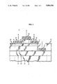
FIG. 1 schematically depicts in cross section an exemplary HBT 10 according to the invention. Exemplarily, transistor 10 is a gallium arsenide-based HBT formed on a semi-insulating (100) GaAs substrate 11. On the substrate, and epitaxial therewith, is subcollector 12, exemplarily a n+ GaAs layer. On the subcollector layer are, in sequence, etch stop layer 20, collector 13, base 14, and emitter 15. All of these are epitaxial with the substrate, as will be readily appreciated by those skilled in the art. On emitter 15 is contact layer 19, with cap layer 18 situated thereon. Patterned metallization regions 23, 16 and 17 serve to provide electrical contact with the emitter, base, and collector, respectively, with the latter contact situated in via hole 21. Ion implanted regions 22 serve to electrically isolate transistor 10 from other devices formed on the same substrate. Such isolation, and means for accomplishing it, are well known to those skilled in the art.
Emitter layer 15 advantageously is very thin, exemplarily between about 5 and 25 nm. More generally, the lower limit of the acceptable thickness is such that under normal operating conditions the reverse tunneling current (i.e., tunneling of holes from the base into contact layer 19) is negligible. The upper level of acceptable thickness of the emitter layer is determined by the condition that the material of the emitter layer be substantially fully depleted of conduction electrons at all bias levels within the normal operating range of the transistor, exemplarily Vbe in the range 0.5-2.0V.
Significantly, as can be seen from FIG. 1, the base contacts 16 are placed on emitter layer 15. Furthermore, the emitter layer 15 is of essentially the same thickness in the extrinsic base region as it is in the intrinsic base region, i.e., that portion that underlies the contact layer 19.
A HBT of the type exemplified by FIG. 1 has significant advantages over prior art devices. For instance, the emitter layer serves both as an etch stop layer and as a passivation layer. The structure can be produced in self-aligned fashion, thereby avoiding critical alignment steps. Due to the thinness of emitter layer 15 it is readily possible to establish ohmic contact to base layer 14 through the emitter. All of the above contribute to making the inventive HBT relatively easily and reliably manufacturable. Furthermore, since base contact is established through the emitter layer it is possible to reliably contact base layers of essentially any thickness, including a base comprising a submonolayer of dopant atoms, such as is disclosed in U. S. Pat. No. 4,825,265.
The details of the epitaxial layer structure of a particular exemplary HBT according to the invention are given in Table I, wherein the numerals in the first column refer to FIG. 1, and wherein the designations n and p refer to the conductivity type of the layer material in the usual way, and "i" stands for "Intrinsic".
                                  TABLE 1
__________________________________________________________________________
Epitaxial Layer Structure Of A
GaAs-based Heterojunction Bipolar Transistor
        Thickness     Doping Alloy
layer   (Å)
              Type    (cm.sup.-3)
                             Composition
__________________________________________________________________________
cap layer 18
        300   In.sub.y Ga.sub.1-y As-n
                      2 × 10.sup.19
                             y = 0.5
cap layer 18
        200   In.sub.y Ga.sub.1-y As-n
                      2 × 10.sup.19
                             y = 0→0.5
contact layer 19
        2000  GaAs-n  5 × 10.sup.18
contact layer 19
        100   Al.sub.x Ga.sub.1-x As-n
                      5 × 10.sup.17
                             x = 0.35→0
emitter 15
        150   Al.sub.x Ga.sub.1-x As-n
                      5 × 10.sup.17
                             x = 0.35
base 14  50   Al.sub.x Ga.sub.1-x As-i
                             x = 0.06
base 14 600   Al.sub.x Ga.sub.1-x As-p
                      2.5 × 10.sup.19
                             x = 0→0.06
collector 13
        3000  GaAs-n  1 × 10.sup.17
collector 13
        1000  GaAs-n  5 × 10.sup.18
etch stop 20
        100   Al.sub.x Ga.sub.1-x As-n
                      5 × 10.sup.18
                             x = 0.3→0
etch stop 20
        100   Al.sub.x Ga.sub.1-x As-n
                      5 × 10.sup.18
                             x = 0→0.3
subcollector 12
        5000  GaAs-n  5 × 10.sup.18
__________________________________________________________________________
As can be seen from Table 1, the base layer incorporates a linear grading of Al to create a quasi electric field to increase transport in this region. This is an optional feature. The doping and thickness of the emitter layer 15 of the exemplary HBT was designed such that the material of the emitter layer is fully depleted above the extrinsic base region because of the Fermi level pinning of the AlGaAs surface. Although the exemplary layer sequence of Table 1 corresponds to a HBT utilizing thermionic emission of electrons into the base, the invention is not so limited. In particular, the invention can be embodied in HBTs with tunnel emission, as will be appreciated by those skilled in the art.
Devices according to the invention can have a wide range of lateral dimensions. However, the invention is most advantageously practiced with devices having relatively small lateral dimensions, typically emitter stripe width of less than 5 μm, frequently less than 1 μm.
FIG. 2 shows the dependence of the current gain upon collector current for two HBTs according to the invention that differ in their emitter size, curve 25 pertaining to a device with 0.3×4 μm2 emitter, and curve 26 to a device with 2.3×10 μm2 emitter. The curves are substantially parallel and both transistors exhibit a peak current gain of about 25. Essentially, the current gain is the same for both transistors at the same collector current density, demonstrating the scalability of inventive HBTs, substantially without current gain degradation.
HBTs according to the invention are exemplarily produced as follows. On a (100) oriented semi-insulating gallium arsenide substrate are grown the desired layers, exemplarily the layers listed in Table 1, by MBE. The active device regions are defined by photoresist and the remaining areas are made semi-insulating by ion implantation, using a sequence of doses and energies, as is well known to those skilled in the art. Next a thin tungsten layer is deposited over the entire wafer. Selected regions of the emitter layer are exposed by a process that comprises metal deposition and lift-off of Ti/Au/Ni and subsequent RIE of the exposed tungsten, using SF6 as the etchant gas. The process further comprises wet chemical etching of the exposed regions of the InGaAs cap layer, and selective removal of the underlying GaAs by RIE with CCl2 F2. The amount of undercut in the last step is controlled by adjusting the RIE conditions. Each of these steps individually is conventional and well understood by those skilled in the art. The base contacts are formed by evaporation and lift-of of AuBe directly over the emitter finger to form self-aligned emitter-base contacts. Next, AuGeNi/Au is evaporated and lifted-off for the collector contact. The base and collector contacts are formed simultaneously by heating the wafer to 420° C. for 10 seconds in a rapid thermal anneal furnace. This heat treatment causes diffusion of base metallization through the thin emitter layer such that a low resistance ohmic contact with the base layer is formed. Finally, contact pads are formed by evaporation of Ti/Au.
In some currently preferred embodiments the p-type dopant is C, since this element has a substantially smaller diffusion coefficient in GaAs (and other III-V semiconductors) than do such prior art dopants as Be. A particularly convenient technique for accomplishing the C-doping involves sublimation of C from a heated carbon filament in an MBE growth chamber. Exemplarily, the filament is machined from a graphite sheet, cut to yield a serpentine shape, with current contact pads on both ends of the filament. The filament is dimensioned to result in a convenient resistance value, exemplarily about 1 ohm. In order to achieve high dopant concentration, the filament typically is heated above about 2000° C.
FIG. 3 gives exemplary data on hole concentration in C-doped GaAs (grown at a rate of 1 μm/hr) as a function of graphite filament current. FIG. 4 shows exemplary data on the carrier concentration in C-doped GaAs as a function of distance from the layer surface, both as grown (curve 40) and after a rapid thermal anneal of 5 seconds at 800° C. (curve 41), and demonstrates the relative absence of diffusion of carbon.
The above discussed use of C-doping of III-V semiconductors makes possible a new processing technology that comprises Be implantation to contact the base, and HBTs comprising a C-doped base and implanted Be base contact means are contemplated.

Claims (7)

We claim:
1. An article comprising a heterojunction bipolar transistor comprising a semiconductor body comprising an emitter region, a collector region, and a base region between the emitter and the collector regions, and further comprising means for making electrical contact with the emitter, base, and collector regions, respectively, with the emitter region comprising first semiconductor material that has a larger bandgap than the base region material and is of the opposite conductivity type from the base region material, the emitter region and base region being epitaxial with each other and with the collector region, associated with the transistor are bias voltages within a normal operating range of the transistor, associated with the emitter region being an emitter stripe width W, associated with the base region being an "extrinsic" base region; CHARACTERIZED IN THAT
(a) the emitter region comprises a layer of first semiconductor material that overlies substantially all of the base region, the thickness of the layer chosen such that the portion of the layer that overlies the extrinsic base region is substantially fully depleted of conduction electrons at all bias voltages within the normal operating range of the transistor; and
(b) the means for making electrical contact to the base region comprise a base contact region on the layer of first semiconductor material that provides an ohmic contact with the base region.
2. The article of claim 1, wherein the thickness of the layer of first material is in the range 5-25 nm, and wherein W≲1 μm.
3. The article of claim 1, wherein the layer of first material serves as a base surface passivation layer and contactingly covers substantially all of the base region.
4. The article of claim 1, wherein the first layer material is selected from the group consisting of doped AlGaAs, AlGaSb, InP, InAlAs, GaAsP, Si, GaP, GaAs, and CdTe, and wherein the base region material is selected from the group consisting of doped GaAs, InGaAs, AlGaAs, GaSb, SiGe, Si, Ge, and HgTe.
5. The article of claim 1, wherein the base contact region on the layer of first semiconductor material is a metallized region.
6. The article of claim 1, wherein the base region is carbon doped, and wherein the base contact region on the layer of first semiconductor material comprises Be-implanted material.
7. The article of claim 1, wherein associated with the emitter stripe is a length, the length being greater than W and defining a first direction, associated with the transistor being a reference plane that bisects the emitter stripe normal to the base region and extends in said first direction, associated with the means for making electrical contact with the emitter region being an emitter contact having a half-width measured in a direction normal to said reference plane, associated with said base contact region being a distance from said reference plane measured in the direction normal to the reference plane, wherein said distance from said reference plane is not substantially greater than said half width.
US07/378,534 1989-07-11 1989-07-11 Heterojunction bipolar transistor Expired - Lifetime US5001534A (en)

Priority Applications (4)

Application Number Priority Date Filing Date Title
US07/378,534 US5001534A (en) 1989-07-11 1989-07-11 Heterojunction bipolar transistor
EP19900307351 EP0408252A3 (en) 1989-07-11 1990-07-05 Heterojunction bipolar transistor
JP2177657A JPH0642492B2 (en) 1989-07-11 1990-07-06 Heterojunction bipolar transistor semiconductor device and manufacturing method thereof
US07/606,003 US5106766A (en) 1989-07-11 1990-10-30 Method of making a semiconductor device that comprises p-type III-V semiconductor material

Applications Claiming Priority (1)

Application Number Priority Date Filing Date Title
US07/378,534 US5001534A (en) 1989-07-11 1989-07-11 Heterojunction bipolar transistor

Related Child Applications (1)

Application Number Title Priority Date Filing Date
US07/606,003 Division US5106766A (en) 1989-07-11 1990-10-30 Method of making a semiconductor device that comprises p-type III-V semiconductor material

Publications (1)

Publication Number Publication Date
US5001534A true US5001534A (en) 1991-03-19

Family

ID=23493499

Family Applications (1)

Application Number Title Priority Date Filing Date
US07/378,534 Expired - Lifetime US5001534A (en) 1989-07-11 1989-07-11 Heterojunction bipolar transistor

Country Status (3)

Country Link
US (1) US5001534A (en)
EP (1) EP0408252A3 (en)
JP (1) JPH0642492B2 (en)

Cited By (30)

* Cited by examiner, † Cited by third party
Publication number Priority date Publication date Assignee Title
US5066926A (en) * 1990-06-26 1991-11-19 Pacific Monolithics Segmented cascode HBT for microwave-frequency power amplifiers
US5105250A (en) * 1990-10-09 1992-04-14 Motorola, Inc. Heterojunction bipolar transistor with a thin silicon emitter
US5208184A (en) * 1991-04-30 1993-05-04 Texas Instruments Incorporated P-n junction diffusion barrier employing mixed dopants
US5250448A (en) * 1990-01-31 1993-10-05 Kabushiki Kaisha Toshiba Method of fabricating a miniaturized heterojunction bipolar transistor
US5266818A (en) * 1989-11-27 1993-11-30 Kabushiki Kaisha Toshiba Compound semiconductor device having an emitter contact structure including an Inx Ga1 -x As graded-composition layer
US5283448A (en) * 1989-11-29 1994-02-01 Texas Instruments Incorporated MESFET with indium gallium arsenide etch stop
US5288660A (en) * 1993-02-01 1994-02-22 Avantek, Inc. Method for forming self-aligned t-shaped transistor electrode
US5321302A (en) * 1990-07-25 1994-06-14 Nec Corporation Heterojunction bipolar transistor having base structure for improving both cut-off frequency and maximum oscillation frequency
US5329151A (en) * 1993-04-09 1994-07-12 At&T Bell Laboratories Semiconductor diode
US5331186A (en) * 1991-03-06 1994-07-19 Kabushiki Kaisha Toshiba Heterojunction bipolar transistor with base electrode having Schottky barrier contact to the emitter
US5378922A (en) * 1992-09-30 1995-01-03 Rockwell International Corporation HBT with semiconductor ballasting
US5477066A (en) * 1992-01-09 1995-12-19 Mitsubishi Denki Kabushiki Kaisha Heterojunction bipolar transistor
US5525817A (en) * 1992-10-16 1996-06-11 Texas Instruments Incorporated Bipolar transistor
US5665614A (en) * 1995-06-06 1997-09-09 Hughes Electronics Method for making fully self-aligned submicron heterojunction bipolar transistor
US5814843A (en) * 1994-12-01 1998-09-29 The Furukawa Electric Co., Ltd. Heterojunction bipolar transistor having a graded-composition base region
US5840612A (en) * 1996-05-13 1998-11-24 Trw Inc. Method of fabricating very high gain heterojunction bipolar transistors
US5907165A (en) * 1998-05-01 1999-05-25 Lucent Technologies Inc. INP heterostructure devices
US6368929B1 (en) 2000-08-17 2002-04-09 Motorola, Inc. Method of manufacturing a semiconductor component and semiconductor component thereof
US6531722B2 (en) 2001-02-26 2003-03-11 Sumitomo Electric Industries, Ltd. Bipolar transistor
US6541346B2 (en) 2001-03-20 2003-04-01 Roger J. Malik Method and apparatus for a self-aligned heterojunction bipolar transistor using dielectric assisted metal liftoff process
US6548838B1 (en) * 1999-09-20 2003-04-15 Matsushita Electric Industrial Co., Ltd. Field-effect transistor, bipolar transistor, and methods of fabricating the same
US20040012036A1 (en) * 2002-04-19 2004-01-22 Kenji Kotani Hetero-junction bipolar transistor and a method for manufacturing the same
US20040016941A1 (en) * 2002-05-13 2004-01-29 Masaki Yanagisawa Hetero-junction bipolar transistor and a manufacturing method of the same
US20040041235A1 (en) * 2002-08-29 2004-03-04 Matsushita Electric Industrial Co. Ltd. Bipolar transistor and method for fabricating the same
KR100440253B1 (en) * 2002-05-31 2004-07-15 한국전자통신연구원 Photoreceiver and method of manufacturing the same
US20070102729A1 (en) * 2005-11-04 2007-05-10 Enicks Darwin G Method and system for providing a heterojunction bipolar transistor having SiGe extensions
US20070105330A1 (en) * 2005-11-04 2007-05-10 Enicks Darwin G Bandgap and recombination engineered emitter layers for SiGe HBT performance optimization
US20070102728A1 (en) * 2005-11-04 2007-05-10 Enicks Darwin G Method and system for controlled oxygen incorporation in compound semiconductor films for device performance enhancement
US20070111428A1 (en) * 2005-11-04 2007-05-17 Enicks Darwin G Bandgap engineered mono-crystalline silicon cap layers for SiGe HBT performance enhancement
US9306042B2 (en) 2014-02-18 2016-04-05 International Business Machines Corporation Bipolar transistor with carbon alloyed contacts

Families Citing this family (6)

* Cited by examiner, † Cited by third party
Publication number Priority date Publication date Assignee Title
US5262335A (en) * 1991-10-08 1993-11-16 Trw Inc. Method to produce complementary heterojunction bipolar transistors
US5231037A (en) * 1992-04-30 1993-07-27 Texas Instruments Incorporated Method of making a power VFET device using a p+ carbon doped gate layer
US5468661A (en) * 1993-06-17 1995-11-21 Texas Instruments Incorporated Method of making power VFET device
FR2692721B1 (en) * 1992-06-17 1995-06-30 France Telecom METHOD FOR PRODUCING A BIPOLAR HETEROJUNCTION TRANSISTOR AND TRANSISTOR OBTAINED.
FR2697945B1 (en) * 1992-11-06 1995-01-06 Thomson Csf Process for etching a heterostructure of group III-V materials.
JP2006303244A (en) * 2005-04-21 2006-11-02 Matsushita Electric Ind Co Ltd Hetero-junction bipolar transistor and its manufacturing method

Citations (4)

* Cited by examiner, † Cited by third party
Publication number Priority date Publication date Assignee Title
US4179308A (en) * 1978-06-23 1979-12-18 Rca Corporation Low cost high efficiency gallium arsenide homojunction solar cell incorporating a layer of indium gallium phosphide
US4794440A (en) * 1983-05-25 1988-12-27 American Telephone And Telegraph Company, At&T Bell Laboratories Heterojunction bipolar transistor
US4825265A (en) * 1987-09-04 1989-04-25 American Telephone And Telegraph Company At&T Bell Laboratories Transistor
US4829343A (en) * 1987-07-17 1989-05-09 American Telephone & Telegraph Company, At&T Bell Laboratories Hot electron transistor

Family Cites Families (1)

* Cited by examiner, † Cited by third party
Publication number Priority date Publication date Assignee Title
JPS627159A (en) * 1985-07-03 1987-01-14 Agency Of Ind Science & Technol Semiconductor device

Patent Citations (4)

* Cited by examiner, † Cited by third party
Publication number Priority date Publication date Assignee Title
US4179308A (en) * 1978-06-23 1979-12-18 Rca Corporation Low cost high efficiency gallium arsenide homojunction solar cell incorporating a layer of indium gallium phosphide
US4794440A (en) * 1983-05-25 1988-12-27 American Telephone And Telegraph Company, At&T Bell Laboratories Heterojunction bipolar transistor
US4829343A (en) * 1987-07-17 1989-05-09 American Telephone & Telegraph Company, At&T Bell Laboratories Hot electron transistor
US4825265A (en) * 1987-09-04 1989-04-25 American Telephone And Telegraph Company At&T Bell Laboratories Transistor

Non-Patent Citations (12)

* Cited by examiner, † Cited by third party
Title
"Dramatic Enhancement in the Gain of a GaAs/AlGaAs Heterostructure Bipolar Transistor by Surface Chemical Passivation," C. J. Sandroff et al., Applied Physics Letters, vol. 51(1), pp. 33-35, 1987.
"Effect of Emitter-Base Spacing on the Current Gain of AlGaAs/GaAs Heterojunction Bipolar Transistors," W-S. Lee et al., IEEE Electron Device Letters, vol. 10, No. 5, May 1989.
"Super-Gain AlGaAs/GaAs Heterojunction Bipolar Transistors Using an Emitter Edge-Thinning Design," Hao-Hsiung Lin and Si-Chen Lee, Applied Physics Letters, vol. 47(8), pp. 839-841, 1985.
"Transport and Related Properties of (Ga,Al)As/GaAs Double Heterostructure Bipolar Junction Transistors," S. Tiwari et al., IEEE Transactions on Electron Devices, vol. ED-34, No. 2, Feb. 1987.
Dramatic Enhancement in the Gain of a GaAs/AlGaAs Heterostructure Bipolar Transistor by Surface Chemical Passivation, C. J. Sandroff et al., Applied Physics Letters, vol. 51(1), pp. 33 35, 1987. *
Effect of Emitter Base Spacing on the Current Gain of AlGaAs/GaAs Heterojunction Bipolar Transistors, W S. Lee et al., IEEE Electron Device Letters, vol. 10, No. 5, May 1989. *
James et al, Appl. Phys. Lett., vol. 26, No. 8, Apr. 15, 1975, "GaAs Concentrator Solar Cells", pp. 467-470.
James et al, Appl. Phys. Lett., vol. 26, No. 8, Apr. 15, 1975, GaAs Concentrator Solar Cells , pp. 467 470. *
Super Gain AlGaAs/GaAs Heterojunction Bipolar Transistors Using an Emitter Edge Thinning Design, Hao Hsiung Lin and Si Chen Lee, Applied Physics Letters, vol. 47(8), pp. 839 841, 1985. *
Transport and Related Properties of (Ga,Al)As/GaAs Double Heterostructure Bipolar Junction Transistors, S. Tiwari et al., IEEE Transactions on Electron Devices, vol. ED 34, No. 2, Feb. 1987. *
Woodall et al., Appl. Phys. Lett., vol. 30, No. 9, May 1, 1977, pp. 492 493, An Isothermal . . . Cells . *
Woodall et al., Appl. Phys. Lett., vol. 30, No. 9, May 1, 1977, pp. 492-493, "An Isothermal . . . Cells".

Cited By (43)

* Cited by examiner, † Cited by third party
Publication number Priority date Publication date Assignee Title
US5266818A (en) * 1989-11-27 1993-11-30 Kabushiki Kaisha Toshiba Compound semiconductor device having an emitter contact structure including an Inx Ga1 -x As graded-composition layer
US5283448A (en) * 1989-11-29 1994-02-01 Texas Instruments Incorporated MESFET with indium gallium arsenide etch stop
US6057567A (en) * 1989-11-29 2000-05-02 Texas Instruments Incorporated Integrated circuit and method
US5250448A (en) * 1990-01-31 1993-10-05 Kabushiki Kaisha Toshiba Method of fabricating a miniaturized heterojunction bipolar transistor
US5066926A (en) * 1990-06-26 1991-11-19 Pacific Monolithics Segmented cascode HBT for microwave-frequency power amplifiers
US5321302A (en) * 1990-07-25 1994-06-14 Nec Corporation Heterojunction bipolar transistor having base structure for improving both cut-off frequency and maximum oscillation frequency
US5105250A (en) * 1990-10-09 1992-04-14 Motorola, Inc. Heterojunction bipolar transistor with a thin silicon emitter
US5331186A (en) * 1991-03-06 1994-07-19 Kabushiki Kaisha Toshiba Heterojunction bipolar transistor with base electrode having Schottky barrier contact to the emitter
US5208184A (en) * 1991-04-30 1993-05-04 Texas Instruments Incorporated P-n junction diffusion barrier employing mixed dopants
US5477066A (en) * 1992-01-09 1995-12-19 Mitsubishi Denki Kabushiki Kaisha Heterojunction bipolar transistor
US5378922A (en) * 1992-09-30 1995-01-03 Rockwell International Corporation HBT with semiconductor ballasting
US5525817A (en) * 1992-10-16 1996-06-11 Texas Instruments Incorporated Bipolar transistor
US5288660A (en) * 1993-02-01 1994-02-22 Avantek, Inc. Method for forming self-aligned t-shaped transistor electrode
US5329151A (en) * 1993-04-09 1994-07-12 At&T Bell Laboratories Semiconductor diode
US5814843A (en) * 1994-12-01 1998-09-29 The Furukawa Electric Co., Ltd. Heterojunction bipolar transistor having a graded-composition base region
US5665614A (en) * 1995-06-06 1997-09-09 Hughes Electronics Method for making fully self-aligned submicron heterojunction bipolar transistor
US5729033A (en) * 1995-06-06 1998-03-17 Hughes Electronics Fully self-aligned submicron heterojunction bipolar transistor
US5840612A (en) * 1996-05-13 1998-11-24 Trw Inc. Method of fabricating very high gain heterojunction bipolar transistors
US5907165A (en) * 1998-05-01 1999-05-25 Lucent Technologies Inc. INP heterostructure devices
US6548838B1 (en) * 1999-09-20 2003-04-15 Matsushita Electric Industrial Co., Ltd. Field-effect transistor, bipolar transistor, and methods of fabricating the same
US20020053683A1 (en) * 2000-08-17 2002-05-09 Hill Darrell G. Method of manufacturing a semiconductor component and semiconductor component thereof
US6368929B1 (en) 2000-08-17 2002-04-09 Motorola, Inc. Method of manufacturing a semiconductor component and semiconductor component thereof
US6855965B2 (en) 2000-08-17 2005-02-15 Freescale Semiconductor, Inc. Method of manufacturing a semiconductor component and semiconductor component thereof
US6531722B2 (en) 2001-02-26 2003-03-11 Sumitomo Electric Industries, Ltd. Bipolar transistor
US6541346B2 (en) 2001-03-20 2003-04-01 Roger J. Malik Method and apparatus for a self-aligned heterojunction bipolar transistor using dielectric assisted metal liftoff process
US6888180B2 (en) 2002-04-19 2005-05-03 Sumitomo Electric Industries, Ltd. Hetero-junction bipolar transistor and a method for manufacturing the same
US20040012036A1 (en) * 2002-04-19 2004-01-22 Kenji Kotani Hetero-junction bipolar transistor and a method for manufacturing the same
US20040016941A1 (en) * 2002-05-13 2004-01-29 Masaki Yanagisawa Hetero-junction bipolar transistor and a manufacturing method of the same
US6885042B2 (en) 2002-05-13 2005-04-26 Sumitomo Electric Industries, Ltd. Hetero-junction bipolar transistor and a manufacturing method of the same
KR100440253B1 (en) * 2002-05-31 2004-07-15 한국전자통신연구원 Photoreceiver and method of manufacturing the same
US7148557B2 (en) * 2002-08-29 2006-12-12 Matsushita Electric Industrial Co., Ltd. Bipolar transistor and method for fabricating the same
US20040041235A1 (en) * 2002-08-29 2004-03-04 Matsushita Electric Industrial Co. Ltd. Bipolar transistor and method for fabricating the same
US20070096151A1 (en) * 2002-08-29 2007-05-03 Matsushita Electric Industrial Co., Ltd. Bipolar transistor and method for fabricating the same
US20070102729A1 (en) * 2005-11-04 2007-05-10 Enicks Darwin G Method and system for providing a heterojunction bipolar transistor having SiGe extensions
US20070105330A1 (en) * 2005-11-04 2007-05-10 Enicks Darwin G Bandgap and recombination engineered emitter layers for SiGe HBT performance optimization
US20070102728A1 (en) * 2005-11-04 2007-05-10 Enicks Darwin G Method and system for controlled oxygen incorporation in compound semiconductor films for device performance enhancement
US20070111428A1 (en) * 2005-11-04 2007-05-17 Enicks Darwin G Bandgap engineered mono-crystalline silicon cap layers for SiGe HBT performance enhancement
US7300849B2 (en) 2005-11-04 2007-11-27 Atmel Corporation Bandgap engineered mono-crystalline silicon cap layers for SiGe HBT performance enhancement
US7439558B2 (en) 2005-11-04 2008-10-21 Atmel Corporation Method and system for controlled oxygen incorporation in compound semiconductor films for device performance enhancement
US7651919B2 (en) 2005-11-04 2010-01-26 Atmel Corporation Bandgap and recombination engineered emitter layers for SiGe HBT performance optimization
US9306042B2 (en) 2014-02-18 2016-04-05 International Business Machines Corporation Bipolar transistor with carbon alloyed contacts
US9490352B2 (en) 2014-02-18 2016-11-08 International Business Machines Corporation Bipolar transistor with carbon alloyed contacts
US10079278B2 (en) 2014-02-18 2018-09-18 International Business Machines Corporation Bipolar transistor with carbon alloyed contacts

Also Published As

Publication number Publication date
JPH0353563A (en) 1991-03-07
JPH0642492B2 (en) 1994-06-01
EP0408252A2 (en) 1991-01-16
EP0408252A3 (en) 1991-06-12

Similar Documents

Publication Publication Date Title
US5001534A (en) Heterojunction bipolar transistor
King et al. Bandgap and transport properties of Si/sub 1-x/Ge/sub x/by analysis of nearly ideal Si/Si/sub 1-x/Ge/sub x//Si heterojunction bipolar transistors
Dumke et al. GaAs GaAlAs heterojunction transistor for high frequency operation
US4889831A (en) Method of forming a high temperature stable ohmic contact to a III-V substrate
Sugii et al. beta-SiC/Si heterojunction bipolar transistors with high current gain
US20040016921A1 (en) High peak current density resonant tunneling diode
US6765242B1 (en) Npn double heterostructure bipolar transistor with ingaasn base region
US5106766A (en) Method of making a semiconductor device that comprises p-type III-V semiconductor material
JPH0797589B2 (en) Method for manufacturing heterojunction bipolar transistor
US4889821A (en) Method of manufacturing a semiconductor device of the hetero-junction bipolar transistor type
US6858509B2 (en) Bipolar transistor with upper heterojunction collector and method for making same
JPH06163567A (en) P-n junction diffusion barrier body
JPH0525389B2 (en)
US4889824A (en) Method of manufacture semiconductor device of the hetero-junction bipolar transistor type
US5285089A (en) Diamond and silicon carbide heterojunction bipolar transistor
US5371378A (en) Diamond metal base/permeable base transistor and method of making same
US20060284282A1 (en) Heterjunction bipolar transistor with tunnelling mis emitter junction
Rao et al. An (Al, Ga) As/GaAs heterostructure bipolar transistor with nonalloyed graded-gap ohmic contacts to the base and emitter
Vaidyanathan et al. Planar, ion-implanted bipolar devices in GaAs
JP2004088107A (en) Heterojunction bipolar transistor(hbt) having improved emitter/base grading structure
Tiwari et al. Heterostructure devices using self-aligned p-type diffused ohmic contacts
US5212103A (en) Method of making a heterojunction bipolar transistor
JPH07273311A (en) Band versus band resonance tunnelling transistor
EP0472262B1 (en) Heterojunction bipolar transistor
US5053346A (en) Method for making a high speed gallium arsenide transistor

Legal Events

Date Code Title Description
AS Assignment

Owner name: AMERICAN TELEPHONE AND TELEGRAPH COMPANY, 550 MADI

Free format text: ASSIGNMENT OF ASSIGNORS INTEREST.;ASSIGNORS:LUNARDI, LEDA M.;MALIK, ROGER J.;RYAN, ROBERT W.;REEL/FRAME:005100/0860;SIGNING DATES FROM 19890710 TO 19890711

Owner name: BELL TELEPHONE LABORATORIES INCORPORATED, 600 MOUN

Free format text: ASSIGNMENT OF ASSIGNORS INTEREST.;ASSIGNORS:LUNARDI, LEDA M.;MALIK, ROGER J.;RYAN, ROBERT W.;REEL/FRAME:005100/0860;SIGNING DATES FROM 19890710 TO 19890711

STCF Information on status: patent grant

Free format text: PATENTED CASE

FPAY Fee payment

Year of fee payment: 4

FEPP Fee payment procedure

Free format text: PAYOR NUMBER ASSIGNED (ORIGINAL EVENT CODE: ASPN); ENTITY STATUS OF PATENT OWNER: LARGE ENTITY

Free format text: PAYER NUMBER DE-ASSIGNED (ORIGINAL EVENT CODE: RMPN); ENTITY STATUS OF PATENT OWNER: LARGE ENTITY

FEPP Fee payment procedure

Free format text: PAYOR NUMBER ASSIGNED (ORIGINAL EVENT CODE: ASPN); ENTITY STATUS OF PATENT OWNER: LARGE ENTITY

FPAY Fee payment

Year of fee payment: 8

FPAY Fee payment

Year of fee payment: 12

AS Assignment

Owner name: AGERE SYSTEMS INC., PENNSYLVANIA

Free format text: ASSIGNMENT OF ASSIGNORS INTEREST;ASSIGNORS:AT&T CORP.;LUCENT TECHNOLOGIES INC.;REEL/FRAME:016301/0651;SIGNING DATES FROM 19960329 TO 20010130