US6858509B2 - Bipolar transistor with upper heterojunction collector and method for making same - Google Patents
Bipolar transistor with upper heterojunction collector and method for making same Download PDFInfo
- Publication number
- US6858509B2 US6858509B2 US10/149,433 US14943302A US6858509B2 US 6858509 B2 US6858509 B2 US 6858509B2 US 14943302 A US14943302 A US 14943302A US 6858509 B2 US6858509 B2 US 6858509B2
- Authority
- US
- United States
- Prior art keywords
- layer
- collector
- base
- emitter
- bipolar transistor
- Prior art date
- Legal status (The legal status is an assumption and is not a legal conclusion. Google has not performed a legal analysis and makes no representation as to the accuracy of the status listed.)
- Expired - Lifetime, expires
Links
- 238000000034 method Methods 0.000 title claims description 22
- 238000005468 ion implantation Methods 0.000 claims abstract description 42
- 239000000463 material Substances 0.000 claims abstract description 42
- 230000035945 sensitivity Effects 0.000 claims abstract description 20
- 239000000758 substrate Substances 0.000 claims abstract description 11
- 238000005530 etching Methods 0.000 claims description 33
- 238000004519 manufacturing process Methods 0.000 claims description 22
- 229910052796 boron Inorganic materials 0.000 claims description 15
- 229910052751 metal Inorganic materials 0.000 claims description 15
- 239000002184 metal Substances 0.000 claims description 15
- ZOXJGFHDIHLPTG-UHFFFAOYSA-N Boron Chemical compound [B] ZOXJGFHDIHLPTG-UHFFFAOYSA-N 0.000 claims description 12
- 239000004065 semiconductor Substances 0.000 claims description 10
- 238000002161 passivation Methods 0.000 claims description 7
- 239000003870 refractory metal Substances 0.000 claims description 6
- 239000011347 resin Substances 0.000 claims description 6
- 229920005989 resin Polymers 0.000 claims description 6
- 125000006850 spacer group Chemical group 0.000 claims description 4
- 229910052737 gold Inorganic materials 0.000 claims description 3
- 229910052698 phosphorus Inorganic materials 0.000 claims description 2
- 230000006399 behavior Effects 0.000 claims 1
- 239000010409 thin film Substances 0.000 claims 1
- 229910001218 Gallium arsenide Inorganic materials 0.000 description 31
- 238000002513 implantation Methods 0.000 description 28
- KRKNYBCHXYNGOX-UHFFFAOYSA-N citric acid Chemical compound OC(=O)CC(O)(C(O)=O)CC(O)=O KRKNYBCHXYNGOX-UHFFFAOYSA-N 0.000 description 15
- 230000015556 catabolic process Effects 0.000 description 9
- 238000006731 degradation reaction Methods 0.000 description 9
- 150000002500 ions Chemical class 0.000 description 8
- 238000001465 metallisation Methods 0.000 description 8
- 238000001020 plasma etching Methods 0.000 description 8
- 229910000530 Gallium indium arsenide Inorganic materials 0.000 description 7
- 238000009825 accumulation Methods 0.000 description 7
- 238000003486 chemical etching Methods 0.000 description 7
- 230000003071 parasitic effect Effects 0.000 description 7
- VEXZGXHMUGYJMC-UHFFFAOYSA-N Hydrochloric acid Chemical compound Cl VEXZGXHMUGYJMC-UHFFFAOYSA-N 0.000 description 6
- 238000000137 annealing Methods 0.000 description 6
- 230000007547 defect Effects 0.000 description 5
- 238000009792 diffusion process Methods 0.000 description 5
- 230000001681 protective effect Effects 0.000 description 5
- 239000000243 solution Substances 0.000 description 5
- 238000002347 injection Methods 0.000 description 4
- 239000007924 injection Substances 0.000 description 4
- 230000006798 recombination Effects 0.000 description 4
- 238000005215 recombination Methods 0.000 description 4
- 229910003910 SiCl4 Inorganic materials 0.000 description 3
- HCHKCACWOHOZIP-UHFFFAOYSA-N Zinc Chemical compound [Zn] HCHKCACWOHOZIP-UHFFFAOYSA-N 0.000 description 3
- UMIVXZPTRXBADB-UHFFFAOYSA-N benzocyclobutene Chemical compound C1=CC=C2CCC2=C1 UMIVXZPTRXBADB-UHFFFAOYSA-N 0.000 description 3
- 150000004767 nitrides Chemical class 0.000 description 3
- -1 oxygen ions Chemical class 0.000 description 3
- FDNAPBUWERUEDA-UHFFFAOYSA-N silicon tetrachloride Chemical compound Cl[Si](Cl)(Cl)Cl FDNAPBUWERUEDA-UHFFFAOYSA-N 0.000 description 3
- 230000008719 thickening Effects 0.000 description 3
- 235000012431 wafers Nutrition 0.000 description 3
- 229910052725 zinc Inorganic materials 0.000 description 3
- 239000011701 zinc Substances 0.000 description 3
- 229910002704 AlGaN Inorganic materials 0.000 description 2
- 229910045601 alloy Inorganic materials 0.000 description 2
- 239000000956 alloy Substances 0.000 description 2
- 239000000969 carrier Substances 0.000 description 2
- 230000008859 change Effects 0.000 description 2
- 238000000151 deposition Methods 0.000 description 2
- 230000008021 deposition Effects 0.000 description 2
- 238000009826 distribution Methods 0.000 description 2
- 230000000694 effects Effects 0.000 description 2
- 238000002955 isolation Methods 0.000 description 2
- 230000007246 mechanism Effects 0.000 description 2
- 229910052760 oxygen Inorganic materials 0.000 description 2
- 230000008569 process Effects 0.000 description 2
- 230000000750 progressive effect Effects 0.000 description 2
- 230000003068 static effect Effects 0.000 description 2
- 239000000126 substance Substances 0.000 description 2
- 238000001039 wet etching Methods 0.000 description 2
- OAICVXFJPJFONN-UHFFFAOYSA-N Phosphorus Chemical compound [P] OAICVXFJPJFONN-UHFFFAOYSA-N 0.000 description 1
- 230000003466 anti-cipated effect Effects 0.000 description 1
- 229910052785 arsenic Inorganic materials 0.000 description 1
- RQNWIZPPADIBDY-UHFFFAOYSA-N arsenic atom Chemical compound [As] RQNWIZPPADIBDY-UHFFFAOYSA-N 0.000 description 1
- 230000009286 beneficial effect Effects 0.000 description 1
- 230000008901 benefit Effects 0.000 description 1
- 230000015572 biosynthetic process Effects 0.000 description 1
- 150000001875 compounds Chemical class 0.000 description 1
- 230000007423 decrease Effects 0.000 description 1
- 230000000593 degrading effect Effects 0.000 description 1
- 206010013395 disorientation Diseases 0.000 description 1
- 238000001312 dry etching Methods 0.000 description 1
- 238000011066 ex-situ storage Methods 0.000 description 1
- 230000001747 exhibiting effect Effects 0.000 description 1
- 229910052731 fluorine Inorganic materials 0.000 description 1
- 239000007789 gas Substances 0.000 description 1
- 229910052734 helium Inorganic materials 0.000 description 1
- 229910052739 hydrogen Inorganic materials 0.000 description 1
- 238000001459 lithography Methods 0.000 description 1
- 229910052750 molybdenum Inorganic materials 0.000 description 1
- 230000007935 neutral effect Effects 0.000 description 1
- 239000001301 oxygen Substances 0.000 description 1
- 239000002245 particle Substances 0.000 description 1
- 230000035515 penetration Effects 0.000 description 1
- 239000011574 phosphorus Substances 0.000 description 1
- 230000009467 reduction Effects 0.000 description 1
- 239000011819 refractory material Substances 0.000 description 1
- 230000000284 resting effect Effects 0.000 description 1
- 230000017105 transposition Effects 0.000 description 1
Images


Classifications
-
- H—ELECTRICITY
- H01—ELECTRIC ELEMENTS
- H01L—SEMICONDUCTOR DEVICES NOT COVERED BY CLASS H10
- H01L29/00—Semiconductor devices adapted for rectifying, amplifying, oscillating or switching, or capacitors or resistors with at least one potential-jump barrier or surface barrier, e.g. PN junction depletion layer or carrier concentration layer; Details of semiconductor bodies or of electrodes thereof ; Multistep manufacturing processes therefor
- H01L29/66—Types of semiconductor device ; Multistep manufacturing processes therefor
- H01L29/66007—Multistep manufacturing processes
- H01L29/66075—Multistep manufacturing processes of devices having semiconductor bodies comprising group 14 or group 13/15 materials
- H01L29/66227—Multistep manufacturing processes of devices having semiconductor bodies comprising group 14 or group 13/15 materials the devices being controllable only by the electric current supplied or the electric potential applied, to an electrode which does not carry the current to be rectified, amplified or switched, e.g. three-terminal devices
- H01L29/66234—Bipolar junction transistors [BJT]
- H01L29/6631—Bipolar junction transistors [BJT] with an active layer made of a group 13/15 material
- H01L29/66318—Heterojunction transistors
-
- H—ELECTRICITY
- H01—ELECTRIC ELEMENTS
- H01L—SEMICONDUCTOR DEVICES NOT COVERED BY CLASS H10
- H01L29/00—Semiconductor devices adapted for rectifying, amplifying, oscillating or switching, or capacitors or resistors with at least one potential-jump barrier or surface barrier, e.g. PN junction depletion layer or carrier concentration layer; Details of semiconductor bodies or of electrodes thereof ; Multistep manufacturing processes therefor
- H01L29/66—Types of semiconductor device ; Multistep manufacturing processes therefor
- H01L29/68—Types of semiconductor device ; Multistep manufacturing processes therefor controllable by only the electric current supplied, or only the electric potential applied, to an electrode which does not carry the current to be rectified, amplified or switched
- H01L29/70—Bipolar devices
- H01L29/72—Transistor-type devices, i.e. able to continuously respond to applied control signals
- H01L29/73—Bipolar junction transistors
- H01L29/737—Hetero-junction transistors
- H01L29/7371—Vertical transistors
Definitions
- the invention relates to a collector-up heterojunction bipolar transistor and its method of production.
- the invention aims to enhance electron transport in heterojunction bipolar transistors (HBT) in collector-up topology, while ensuring a high production yield.
- HBT heterojunction bipolar transistors
- the collector-up configuration is particularly beneficial in the case of a heterojunction bipolar transistor because of the low values of base-collector capacitance which it makes it possible to obtain by comparison with those encountered with a conventional topology, called emitter-up topology.
- the reduction in this junction capacitance especially makes it possible to enhance the UHF performance of this type of component.
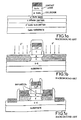
- FIG. 1 shows the manufacturing method used by Yamahata et al.
- a metal collector contact is deposited on the epitaxial structure. It is used as a mask for etching the collector layer ( FIG. 1 a ).
- the structure is then implanted with oxygen ions through the base with an energy which is determined so as to render the extrinsic emitter regions ( FIG. 1 b ) electrically isolating.
- a zinc diffusion makes it possible to re-establish a sufficient level of p + doping of the base layer which was damaged during the ion implantation ( FIG. 1 c ).
- the metal base contacts are then deposited.
- the base and emitter layers are then etched in order to deposit metal emitter contacts on an n + doped sub-emitter.
- the component thus produced exhibits low base-collector capacitance and a heavily doped base.
- Such a manufacturing method exhibits certain drawbacks.
- the base is severely damaged during the stage of oxygen-ion implantation. This is because, with the wafer being disoriented by 7° with respect to the direction of the implantation beam, it is therefore seen by the latter in a quasi-amorphous state.
- the number of crystalline defects generated in the base is therefore a maximum.
- the zinc diffusion makes it possible partly to mask this degradation, but does not make it possible to regain the initial conductivity of the base.
- the flanks of the collector mesa have to be protected by a nitride which induces a lithography stage and a supplementary process stage.
- the surface area of the intrinsic active area is defined, therefore limited, by the size of the collector. It should be noted that, because of the high diffusion of the zinc, there exists a substantial risk of seeing short-circuits appear at the base-emitter junction, having a devastating impact on the reliability of the components.
- the THOMSON-CSF Central Research Laboratory started to produce GaInP/GaAs heterojunction bipolar transistors (D-HBT) in collector-up technology, as described in the article by HENKEL et al., IEEE Electronics Letters, Vol. 33, No. 7, March 1997.
- the emitter region situated below the extrinsic base is, here again, converted into a highly resistive layer, but by an ion implantation which is optimized with a view to keeping the base at its initial conductivity.
- FIG. 2 shows the manufacturing method used.
- a metal collector contact is first of all deposited on the epitaxial structure. It is used as a mask for etching the collector layer ( FIG. 2 a ).
- the structure is then implanted with boron ions through the base, and at a low dose ( FIG. 2 b ).
- the angle of implantation is 0° so as to minimize the collisions between the boron ions and the crystalline lattice of the base.
- the metal base contacts are then deposited.
- the base and emitter layers are then etched in order to deposit metal emitter contacts ( FIG. 2 c ) on an n + doped sub-emitter. These contacts then undergo annealing (416° C.
- This manufacturing process makes it possible, in a very effective way, to isolate the extrinsic emitter areas electrically while maintaining the conductivity of the base layer at a value close to its initial value.
- This latter property is, on the one hand, related to the fact that the implantation is done at lower dose.
- the number of crystalline defects generated in the base is therefore minimized.
- the wafer is no longer disorientated with respect to the direction of the implantation beam (angle of implantation zero), the ions implanted are thus channeled into the crystalline network.
- the possibilities of a collision between an incident boron particle and the atoms and the electrons constituting the base material are then reduced.
- the same goes for the number of crystalline defects generated in the base.
- the zinc-diffusion stage proposed by Hyundaita et al. is then superfluous, bringing about simplification of the manufacturing method.
- the collector-up topology amounts to being placed in the most unfavorable of the preceding two cases. This is because, in this structure, the surface area of the collector at the base-collector junction defines the active area of the component. The extrinsic collector areas are therefore non-existent and can be modeled by a perfect insulant. In this configuration, if the surface area of the base-collector junction is less than that of the emitter-base junction, the phenomenon of electron accumulation in the extrinsic-base regions is particularly significant. The same goes for the emitter-up topology; the optimal performance is obtained when the surface area of the emitter-base junction is the smaller of the two. The production of high-performance collector-up components therefore requires perfect control of the techniques of implantation and of etching which will culminate in the definition of the surface areas of the two junctions.
- the etching of the collector mesa is based on the selectivity of etching between the two materials constituting collector and base (the case of the D-HBT) or base and etching-stop layer (the case of the S-HBT).
- the metal collector contact is used as a mask for etching the collector. The surface area of this contact therefore defines that of the base-collector junction plus or minus the sub-etching (if any).
- FIG. 3 shows the etching profile which is obtained according to the crystalline orientation for a collector made of GaInP (the case of the D-HBT).
- This profile is conventionally obtained by chemical etching (for example by the use of hydrochloric acid, diluted or otherwise). It will be noted that, depending on the crystalline orientation, a re-entrant or outgoing angle is observed.
- the example is taken for the case of a GaAs substrate (100) oriented according to the European/Japanese standard for indexing wafers. The shape indicated is obtained very simply with the condition that the layer of GaInP is sufficiently fine (of the order of 0.5 ⁇ m).
- the flanks of the collector mesa are re-entrant ( FIG. 4 a ). If x is defined as the difference between the width of the extrinsic collector (defined by the etching) and that of the extrinsic emitter (defined by the shape of the isolating wells), x is then negative and on the order of ⁇ 0.2 ⁇ m.
- the emitter-base junction therefore exhibits a surface area greater than that of the base-collector junction, and x is sufficiently large enough to entail a substantial degradation in the current gain and in f t .
- the etching profile is then outgoing.
- the flanks of the collector mesa which are not protected by the collector metalization, are then exposed to the ion implantation with boron. This gives rise to the appearance of isolating wells in the emitter 1 , and also in the collector 2 ( FIG. 4 b ).
- the width of the extrinsic collector is no longer defined by etching but by the shape of the collector-isolating wells.
- x is then negative, but small in absolute value. The degradation in the current gain and in f, is then less significant than in the preceding case, but is still present, however.
- the etching of a collector made of GaAs (case of the S-HBT) is carried out in two operations: a reactive-ion etching (such as SiCl 4 ) followed by a chemical etching (with citric acid, for example).
- a reactive-ion etching such as SiCl 4
- a chemical etching with citric acid, for example.
- a chemical etching of the stop layer is then carried out using a solution which may be based, for example, on dilute hydrochloric acid.
- a solution which may be based, for example, on dilute hydrochloric acid.
- the profile obtained does not depend on the crystalline orientation and exhibits an outgoing angle associated with a sub-etching at the interface with the ohmic contact ( FIG. 4 c ).
- the width of the extrinsic collector is therefore defined by the etching flanks and x is, here again, negative but small in absolute value.
- the degradation in the current gain and in f t is substantially the same as in the preceding case.
- the present invention aims to reach these performance levels by optimizing the collection of the minority carriers at the exit from the base, that is to say by getting round the accumulation of electrons in the extrinsic-base regions. To do that, it is necessary to be able to define a base-collector junction the surface area of which is larger than that of the emitter-base junction, and for the extrinsic collector, if it exists, to be made from a semi-isolating material.
- the invention therefore relates to a collector-up heterojunction bipolar transistor that includes, stacked on a substrate:
- the invention also relates to a method of manufacturing a collector-up heterojunction bipolar transistor including the epitaxial growth of semiconducting layers on a semiconductor substrate:
- FIGS. 1 a to 4 c various states of the technique described in the foregoing;
- FIGS. 6 and 7 an example embodiment of an HBT transistor according to the invention.
- FIG. 8 a variant embodiment of an HBT transistor according to the invention.
- FIGS. 9 a to 9 l an example of an embodiment method, according to the invention, of a collector-up HBT transistor.
- the principle of the present invention is based, on the one hand, on the selectivity of etching between the two materials constituting collector and base (the case of the D-HBT) or etching-stop layer and base (the case of the S-HBT), and, on the other hand, on the differing sensitivity of the conductivity of the semiconductor materials subjected to an ion implantation.
- the etching profile of the GaInP depends heavily on the crystalline orientation. Depending on the crystallographic direction along which the collector electrode is oriented, the flanks of the collector mesa exhibit a re-entrant or outgoing angle. It is reiterated that the lateral dimension of the device is then fixed by that of the contact layer in the n + GaAs, the etching of the GaInP being blocked at the interface of the two materials.
- FIGS. 5 a and 5 b show, by way of example, the difference in sensitivity of the electrical conductivity of the n-doped GaInP and of the p + doped GaAs respectively, to a boron implantation at 200 keV at zero angle of implantation, as a function of the dose of ions input into the structure. This progressive change is continued as a function of the annealing time at 416° C.
- the material exhibits an electrical resistivity greater than 10 5 ⁇ .cm for an implantation dosage of 5 ⁇ 10 12 cm ⁇ 2
- the p + type GaAs remains practically insensitive to the ion implantation up to dosages of 10 13 cm ⁇ 2 .
- FIG. 6 shows the sectional view of a collector-up D-HBT designed in the light of the present invention.
- the surfaces of the emitter-base and the base-collector junctions are then defined during the ion-implantation stage. It will be noted that there is formed, on either side of the collector mesa, before deposition of the base contact, an isolating well equivalent to a side wall, which makes it possible to reduce the presence of metalization on the bared flanks of the collector mesa.
- the device of the invention relates to a collector-up HBT transistor which particularly includes an emitter layer EM, base layer BA and collector layer CO stack, in which the collector and the emitter are self-aligned by implantation and in which:
- the collector spigot (electrode) is oriented along the crystallographic direction ⁇ 0 1 1> in such a way that, during the etching stage, the flanks of the collector layer made electrically isolating exhibit re-entrant angles.
- a GaInAs contact layer at the peak of the epitaxial structure makes it possible to form the ohmic contact lead by the use of a refractory metal such as TiWSi, WN, or TiW, etc.
- metalization by Ti/Pt/Au typically 2 ⁇ m wide and with a thickness of the order of 1 ⁇ m, is deposited on the surface.
- the semiconductor materials protected by this metal mask have their initial electrical conductivity preserved.
- the thickness of the metalization of refractory metal is sufficiently fine to allow the ions to pass through it without major loss of energy.
- the implantation stage is divided into two operations using the same metal mask. One of the two operations consists in carrying out an implantation at high energy, low dosage (2.5 ⁇ 10 12 cm ⁇ 2 ), through the whole of the structure, and which can be at zero implantation angle.
- the energy supplied to the implanted ions is calculated in such a way as to render the GaInP emitter layer isolating in the areas situated under the future extrinsic base (isolating wells 1 and 2) so as to eliminate any parasitic injection of electrons.
- the other operation consists in defining the surface area of the base-collector junction via an implantation at lower energy, low dose and through the whole of the structure.
- the isolating wells 3 and 4 are thus created locally in the GaInP collector layer.
- the distribution tail of the ions then passes through the base without really degrading it because of the low sensitivity of the p + GaAs material to the implantation.
- the slight increase in the resistivity of the base material is compensated for during a post-implantation annealing stage (which can be that for annealing the alloyed ohmic contact, for example) making it possible to bring the concentration of crystalline defects down to the lowest possible level.
- a post-implantation annealing stage which can be that for annealing the alloyed ohmic contact, for example
- the use of a refractory material offers the possibility of annealing the structure at high temperatures (if necessary) after definition of the collector mesa.
- FIG. 7 represents the profile which will typically be obtained on conclusion of the implantation stage; x, defined as in FIG. 4 , is of the order of +0.2 ⁇ m.
- the present invention therefore allows us to eliminate the accumulation of the electrons in the extrinsic base region and thus to come close to the optimal performance levels allowed by the structure of the component.
- the collector mesa should typically be of the order of 1 ⁇ m on each side of the Ti/Pt/Au collector strip so as to achieve effective collection of the electrons at the exit from the base.
- the width of 1 ⁇ m makes it possible to find an effective compromise so as to produce components functioning at UHF.
- the UHF gain tends, in effect, to drop when the edge of the base ohmic contact strip is moved away from the active emitter area, since there is then an increase in the base resistance and the base-collector capacitance.
- the ohmic base contact can be produced in self-alignment with respect to the collector mesa.
- the present invention can also be associated with a more conventional fine ledge-type passivation layer as described in the French patent No 2 736 468.
- An example of a component produced with this invention associated with a conventional thin ledge is given in FIG. 8 .
- the manufacturing method used for the present invention is then directly adaptable.
- the epitaxial structure remains identical, only the sequential linking of the manufacturing stages is altered.
- this invention can use a heat sink making it possible to remove some of the heat energy through the top of the structure. It may be of the “nitride” type like the one previously patented (French patent No. 2 737 342) or arise from any other similar method.
- the refractory ohmic contact can be replaced by a Schottky-type contact.
- a metal contact Ti/Pt/Au, for example
- Ti/Pt/Au for example
- the contact layer n + GaInAs on n ⁇ GaAs
- the epitaxial structure is thus simplified.
- the metal contact via its high thermal conductivity, promises to offer better thermal behavior.
- FIG. 9 a
- a spacer made from a layer of n-doped GaAs associated or not associated with a layer of n-doped GaInP, or a gradual layer of n-doped Ga x In 1-x As y P 1-y may be inserted between base and collector (or even between emitter and base) in order to minimize the phenomenon of electron accumulation in the potential well of each of the heterojunctions.
- This spacer is not represented here.
- a refractory-metal layer is deposited ex-situ so as to provide the collector refractory ohmic contact.
- a stage of electrical-isolation deep ion (H, He, B, O, F, etc) implantation is carried out, so as to reduce the parasitic effects in the component and to achieve inter-component isolation.
- Deposition of a metalization for thickening of the collector ohmic contact of width l c is then carried out by lift-off (Ti/Au, Ti/Pt/Au, etc), and then selective ion implantation is carried out with boron at high energy, in such a way as to define the isolating wells 1 and 2 in the extrinsic emitter areas.
- This implantation stage leads inherently to the defining of the shape of the intrinsic emitter and thus to that of the surface of the emitter-base junction.
- the structure is implanted with boron, but at lower energy so as to define the isolating wells 3 and 4 in the extrinsic collector areas.
- This implantation stage leads inherently to the definition of the shape of the intrinsic collector and thus to that of the surface of the base-collector junction.
- the surface implanted within the emitter-base junction is larger than that of the collector-base junction.
- the surface area of the base/collector junction is greater than the surface area of the base/emitter junction.
- the metalization for thickening of the collector contact is again used as a protective mask.
- a dry etching of the refractory metal is then carried out by reactive-ion etching based on SF 6 , for example.
- the collector mesa is defined.
- a protective mask of resin with a width L C >l C is produced.
- Etching of the GaInAs contact layer is carried out by wet etching based on citric acid, then etching of the GaAs contact layer is carried out by chlorinated reactive-ion etching (RIE) such as SiCl 4 , or by chemical etching using citric acid, for example, and of the collector layer made of GaInP implanted with boron in chemical etching mode based on hydrochloric acid.
- RIE reactive-ion etching
- the base ohmic contacts are deposited by lift-off technique.
- the metal film used can be made from an alloy of Ti/Pt/Au or Mo/Au, for example.
- a protective mask is produced from resin, having a width L B >Lc, then the etching of the base mesa is carried out by the dry method (chlorinated reactive-ion etching) or combined (RIE then chemical) etching, followed by the etching of the GaInP emitter layer implanted with boron in chemical etching mode based on hydrochloric acid.
- the etching of the GaInP is blocked at the GaAs/GaInP interface.
- the lateral dimension of the base mesa thus fixes that of the emitter mesa.
- the emitter ohmic contacts are deposited using the lift-off technique.
- etching of the GaInAs contact layer is carried out by wet etching based on citric acid, then etching of the GaAs contact layer is carried out by chlorinated reactive ion etching (RIE) such as SiCl 4 , or by chemical etching by the use of citric acid, for example.
- RIE reactive ion etching
- a passivation dielectric layer protecting the whole of the surface of the component ( FIG. 9 j ) is carried out.
- Such a heat sink can be based on a pillars/beams technique as represented in FIG. 9 j .
- the air present under the beam can be replaced by a dielectric possessing good planarisation properties such as benzocyclobutene (BCB) for example, which makes it possible, from the point of view of its mechanical properties, to reinforce the structure particularly with a view to offset operations.
- BCB benzocyclobutene
- FIG. 9 k presents the sectional view of an HBT using a heat sink of the “double nitride” type.
- the heat sink covers the whole of the component and does not use bridges (in air, in BCB, etc).
- the stage of producing the pillars is dispensed with, the removal of the heat energy, and thus the thermal behavior of the component, are optimal.
- a slight degradation in the value of certain parasitic elements should be anticipated (increase in the parasitic collector capacitance, for example), a degradation possibly slightly influencing the UHF behavior of the component.
Abstract
A collector-up heterojunction bipolar transistor including, stacked on a substrate, an emitter layer, a base layer, and a collector layer. In this transistor the surface area of the base-emitter junction is of smaller dimensions than the surface area of the base-collector junction. Further, the material of the base layer exhibits a sensitivity of the electrical conductivity to ion implantation that is lower than the sensitivity of the electrical conductivity of the material of the emitter layer to the same ion implantation.
Description
1. Field of the Invention
The invention relates to a collector-up heterojunction bipolar transistor and its method of production.
The invention aims to enhance electron transport in heterojunction bipolar transistors (HBT) in collector-up topology, while ensuring a high production yield.
2. Description of the Background
The collector-up configuration is particularly beneficial in the case of a heterojunction bipolar transistor because of the low values of base-collector capacitance which it makes it possible to obtain by comparison with those encountered with a conventional topology, called emitter-up topology. The reduction in this junction capacitance especially makes it possible to enhance the UHF performance of this type of component.
In contrast, if a few specific precautions are not taken, parasitic injection of electrons into the extrinsic base areas appears in an HBT. These electrons are then picked up by the base contacts or recombine in the extrinsic base; which, in both cases, leads to a degradation of the transport factor in the base and thus heavily penalizes the current gain of the transistor. Certain solutions have already been applied to this problem, and especially in the case of collector-up HBTs fabricated with GaAlAs/GaAs or GaInP/GAs materials.
Thus Yamahata et al. describe, in a publication (IEEE Electron Device Letters, Vol. 14, No 4, April 1993) a GaAlAs/GaAs collector-up single heterojunction bipolar transistor (S-HBT) in which the emitter region situated above the extrinsic base is converted into a highly resistive layer by ion implantation. In this way, it gets around the parasitic injection of electrons mentioned above and, at the same time, enhances the current gain of the HBT thus produced.
Such a manufacturing method exhibits certain drawbacks. First of all, the base is severely damaged during the stage of oxygen-ion implantation. This is because, with the wafer being disoriented by 7° with respect to the direction of the implantation beam, it is therefore seen by the latter in a quasi-amorphous state. The number of crystalline defects generated in the base is therefore a maximum. The zinc diffusion makes it possible partly to mask this degradation, but does not make it possible to regain the initial conductivity of the base. Moreover, during stages of implantation and of diffusion, the flanks of the collector mesa have to be protected by a nitride which induces a lithography stage and a supplementary process stage. With this method, the surface area of the intrinsic active area is defined, therefore limited, by the size of the collector. It should be noted that, because of the high diffusion of the zinc, there exists a substantial risk of seeing short-circuits appear at the base-emitter junction, having a devastating impact on the reliability of the components.
The THOMSON-CSF Central Research Laboratory started to produce GaInP/GaAs heterojunction bipolar transistors (D-HBT) in collector-up technology, as described in the article by HENKEL et al., IEEE Electronics Letters, Vol. 33, No. 7, March 1997. The emitter region situated below the extrinsic base is, here again, converted into a highly resistive layer, but by an ion implantation which is optimized with a view to keeping the base at its initial conductivity.
This manufacturing process, based on the different sensitivity of the conductivity of different semiconductor materials subjected to the same ion implantation, makes it possible, in a very effective way, to isolate the extrinsic emitter areas electrically while maintaining the conductivity of the base layer at a value close to its initial value. This latter property is, on the one hand, related to the fact that the implantation is done at lower dose. The number of crystalline defects generated in the base is therefore minimized. Moreover, the wafer is no longer disorientated with respect to the direction of the implantation beam (angle of implantation zero), the ions implanted are thus channeled into the crystalline network. The possibilities of a collision between an incident boron particle and the atoms and the electrons constituting the base material are then reduced. The same goes for the number of crystalline defects generated in the base. Moreover, the zinc-diffusion stage proposed by Yamahata et al. is then superfluous, bringing about simplification of the manufacturing method.
This particularly advantageous manufacturing method exhibits certain limitations, however. This is because, whereas the UHF performance of this type of component is particularly attractive (Fmax=115 GHz), the value of the static current gain obtained is low. In order to analyze this behavior, we have to recall the results of the work by HORIO et al., published in IEEE Transactions on Electron Devices, Vol. 42, No. 11, November 1995.
The work by HORIO et al. bears on emitter-up HBT devices produced with GaAlAs/GaAs materials. This work highlighted an accumulation of electrons in the extrinsic base regions in the case in which the emitter-up HBT features an extrinsic collector made perfectly isolating and a surface area of the base-collector junction slightly less than that of the emitter-base junction. From this accumulation there results, on the one hand, a degradation in the cut-off frequency of the current gain ft and, on the other hand, a recombination of the carriers in the base which will heavily penalize the static gain of the transistor. In the case of a structure which is similar but featuring a semi-isolating extrinsic collector (which corresponds to an extrinsic collector electrically isolated by ion implantation), the phenomenon of electron accumulation seems much more limited, and therefore the degradations in the current gain and in ft become much smaller. Moreover, Horio observes that the performance of the component is optimal when the surface area of the emitter-base junction is slightly less than that of the base-collector junction, and is so whatever the nature of the extrinsic collector (isolating or semi-isolating).
Unfortunately, the collector-up topology amounts to being placed in the most unfavorable of the preceding two cases. This is because, in this structure, the surface area of the collector at the base-collector junction defines the active area of the component. The extrinsic collector areas are therefore non-existent and can be modeled by a perfect insulant. In this configuration, if the surface area of the base-collector junction is less than that of the emitter-base junction, the phenomenon of electron accumulation in the extrinsic-base regions is particularly significant. The same goes for the emitter-up topology; the optimal performance is obtained when the surface area of the emitter-base junction is the smaller of the two. The production of high-performance collector-up components therefore requires perfect control of the techniques of implantation and of etching which will culminate in the definition of the surface areas of the two junctions.
In the case of heterojunction bipolar transistors in collector-up topology, the etching of the collector mesa is based on the selectivity of etching between the two materials constituting collector and base (the case of the D-HBT) or base and etching-stop layer (the case of the S-HBT). The metal collector contact is used as a mask for etching the collector. The surface area of this contact therefore defines that of the base-collector junction plus or minus the sub-etching (if any).
Thus, for a D-HBT in which the collector spigot is oriented along the crystallographic direction <0 1 1>, the flanks of the collector mesa are re-entrant (FIG. 4 a). If x is defined as the difference between the width of the extrinsic collector (defined by the etching) and that of the extrinsic emitter (defined by the shape of the isolating wells), x is then negative and on the order of −0.2 μm. The emitter-base junction therefore exhibits a surface area greater than that of the base-collector junction, and x is sufficiently large enough to entail a substantial degradation in the current gain and in ft.
If the collector electrode of the D-HBT is oriented along the crystallographic direction <0 1 −1>, the etching profile is then outgoing. The flanks of the collector mesa, which are not protected by the collector metalization, are then exposed to the ion implantation with boron. This gives rise to the appearance of isolating wells in the emitter 1, and also in the collector 2 (FIG. 4 b). The width of the extrinsic collector is no longer defined by etching but by the shape of the collector-isolating wells. x is then negative, but small in absolute value. The degradation in the current gain and in f, is then less significant than in the preceding case, but is still present, however.
The etching of a collector made of GaAs (case of the S-HBT) is carried out in two operations: a reactive-ion etching (such as SiCl4) followed by a chemical etching (with citric acid, for example). This is because, in order not to damage the base material, advantage can be taken of the existence of the very wide selectivity of etching between a phosphorus-based layer and an arsenic-based layer. An etching-stop layer of shallow thickness is therefore added between the collector (n GaAs) and the base (p+ GaAs). Made for example from GaInP, it makes it possible to stop the etching of the collector made of GaAs. A chemical etching of the stop layer is then carried out using a solution which may be based, for example, on dilute hydrochloric acid. On completion of this sequence, the profile obtained does not depend on the crystalline orientation and exhibits an outgoing angle associated with a sub-etching at the interface with the ohmic contact (FIG. 4 c). The width of the extrinsic collector is therefore defined by the etching flanks and x is, here again, negative but small in absolute value. The degradation in the current gain and in ft is substantially the same as in the preceding case.
Thus, solutions have been applied in order to get around the parasitic injection of electrons into the extrinsic base which constitutes the most significant difficulty in the production of collector-up HBTs. Among these, the production of isolating wells in the extrinsic emitter by ion implantation at low dose through the base makes it possible, furthermore, to keep the latter at its initial conductivity. However, as we have been able to see, it is not possible, in the case of the manufacture of collector-up HBTs consisting of GaxIn1-xAs/GayIn1-yP compounds, to define the surface areas of the emitter-base and base-collector junctions in such a way as to obtain the optimal performance capable of being reached with such structures. The present invention aims to reach these performance levels by optimizing the collection of the minority carriers at the exit from the base, that is to say by getting round the accumulation of electrons in the extrinsic-base regions. To do that, it is necessary to be able to define a base-collector junction the surface area of which is larger than that of the emitter-base junction, and for the extrinsic collector, if it exists, to be made from a semi-isolating material.
The invention therefore relates to a collector-up heterojunction bipolar transistor that includes, stacked on a substrate:
-
- an emitter layer
- a base layer
- a collector layer
- characterized in that:
- the surface area of the base-emitter active junction is of smaller dimensions than the surface area of the base-collector active junction;
- the material of the base layer exhibits a sensitivity of the electrical conductivity to ion implantation which is lower than the sensitivity of the electrical conductivity of the material of the emitter layer to the same ion implantation.
The invention also relates to a method of manufacturing a collector-up heterojunction bipolar transistor including the epitaxial growth of semiconducting layers on a semiconductor substrate:
-
- an emitter layer
- a base layer
- a collector layer
- characterized in that:
- the materials of the base layer and of the emitter layer are chosen such that the material of the base layer exhibits a sensitivity of the electrical conductivity to ion implantation which is lower than the sensitivity of the electrical conductivity of the emitter layer to the same ion implantation.
- and in that it includes the following additional stages:
- production of a mask on the collector layer, having a width (lc) defining the width of the collector to be obtained, then carrying out a first ion implantation making it possible to render the material of the emitter layer isolating on either side of the emitter to be obtained, then carrying out a second ion implantation using one or more energies which are lower than the first ion implantation, so as to render the material of the collector layer isolating on either side of the collector to be obtained.
The various objects and characteristics of the invention will emerge more clearly in the description which will follow, given by way of example, as well as from the annexed figures. These figures represent:
In general, the principle of the present invention is based, on the one hand, on the selectivity of etching between the two materials constituting collector and base (the case of the D-HBT) or etching-stop layer and base (the case of the S-HBT), and, on the other hand, on the differing sensitivity of the conductivity of the semiconductor materials subjected to an ion implantation.
By way of example, the invention is described in the context of NPN Ga0.5In0.5P/GaAs double-heterojunction bipolar transistors in collector-up topology. However, it applies by simple transposition to any heterojunction bipolar transistor structure in collector-up topology using GaxIn1-xAs/GayIn1-yP heterostructures whether the material constituting the collector is different from that of the base (case of the D-HBT) or identical (give or take the doping characteristics, in the case of the S-HBT). It is also applicable to a number of components in the course of development (SiC/GaN, AlGaN/GaN, AlGaN/InGaN, etc.).
As we have described above in FIG. 3 , the etching profile of the GaInP depends heavily on the crystalline orientation. Depending on the crystallographic direction along which the collector electrode is oriented, the flanks of the collector mesa exhibit a re-entrant or outgoing angle. It is reiterated that the lateral dimension of the device is then fixed by that of the contact layer in the n+ GaAs, the etching of the GaInP being blocked at the interface of the two materials.
By virtue of these physical/chemical properties, it is possible to produce components exhibiting, on either side of the base, a semiconductor layer which is rendered locally electrically isolating by ion implantation. FIG. 6 shows the sectional view of a collector-up D-HBT designed in the light of the present invention. The surfaces of the emitter-base and the base-collector junctions are then defined during the ion-implantation stage. It will be noted that there is formed, on either side of the collector mesa, before deposition of the base contact, an isolating well equivalent to a side wall, which makes it possible to reduce the presence of metalization on the bared flanks of the collector mesa.
Hence it is seen that the device of the invention relates to a collector-up HBT transistor which particularly includes an emitter layer EM, base layer BA and collector layer CO stack, in which the collector and the emitter are self-aligned by implantation and in which:
-
- the emitter layer EM includes the intrinsic emitter itself framed by isolating material, likewise the collector layer CO includes the collector framed by isolating material;
- the surface area of the base emitter junction is less than the surface area of the base collector junction;
- the material of the base BA is such that it exhibits a sensitivity of the electrical conductivity to an isolating ion implantation which is less than the sensitivity of the electrical conductivity of the material of the emitter EM to the same implantation.
The method according to the invention of producing such a device will now be described.
The collector spigot (electrode) is oriented along the crystallographic direction <0 1 1> in such a way that, during the etching stage, the flanks of the collector layer made electrically isolating exhibit re-entrant angles. A GaInAs contact layer at the peak of the epitaxial structure makes it possible to form the ohmic contact lead by the use of a refractory metal such as TiWSi, WN, or TiW, etc. In order to obtain low collector resistance and to produce an effective ion-implantation mask, metalization by Ti/Pt/Au, typically 2 μm wide and with a thickness of the order of 1 μm, is deposited on the surface. The semiconductor materials protected by this metal mask have their initial electrical conductivity preserved. The thickness of the metalization of refractory metal is sufficiently fine to allow the ions to pass through it without major loss of energy. The implantation stage is divided into two operations using the same metal mask. One of the two operations consists in carrying out an implantation at high energy, low dosage (2.5×1012 cm−2), through the whole of the structure, and which can be at zero implantation angle. The energy supplied to the implanted ions is calculated in such a way as to render the GaInP emitter layer isolating in the areas situated under the future extrinsic base (isolating wells 1 and 2) so as to eliminate any parasitic injection of electrons. The other operation consists in defining the surface area of the base-collector junction via an implantation at lower energy, low dose and through the whole of the structure. The isolating wells 3 and 4 are thus created locally in the GaInP collector layer. During these stages, the distribution tail of the ions then passes through the base without really degrading it because of the low sensitivity of the p+ GaAs material to the implantation. The slight increase in the resistivity of the base material is compensated for during a post-implantation annealing stage (which can be that for annealing the alloyed ohmic contact, for example) making it possible to bring the concentration of crystalline defects down to the lowest possible level. It should be noted that the use of a refractory material offers the possibility of annealing the structure at high temperatures (if necessary) after definition of the collector mesa.
It will be noted that the higher the energy supplied to the implanted ions, the greater is their depth of penetration, and also the more spread out is the final distribution of the ions in the bulk (and, thereby, of the crystalline defects which they engender). Hence the surface area of the emitter-base junction (defined by the implantation at high energy) will be smaller than that of the base-collector junction (defined by an implantation at lower energy). FIG. 7 represents the profile which will typically be obtained on conclusion of the implantation stage; x, defined as in FIG. 4 , is of the order of +0.2 μm. The present invention therefore allows us to eliminate the accumulation of the electrons in the extrinsic base region and thus to come close to the optimal performance levels allowed by the structure of the component.
The collector mesa should typically be of the order of 1 μm on each side of the Ti/Pt/Au collector strip so as to achieve effective collection of the electrons at the exit from the base. The width of 1 μm makes it possible to find an effective compromise so as to produce components functioning at UHF. The UHF gain tends, in effect, to drop when the edge of the base ohmic contact strip is moved away from the active emitter area, since there is then an increase in the base resistance and the base-collector capacitance. It is possible to minimize the influence of the latter by etching the refractory-metal layer, and by etching, or isolating by implantation at high dosage, the n+ GaAs and GaInAs contact layer, above the collector-isolating wells. And by taking certain specific precautions, the ohmic base contact can be produced in self-alignment with respect to the collector mesa.
Moreover, such dimensions of the collector mesa remain compatible with the thick-ledge passivation method described in the French patent No (2 764 118). This is because at least two mechanisms are acting on the drift of the HBTs in the course of operation. It is a question, on the one hand, of the progressive change in the recombinations in the neutral base and, on the other hand, of an increase in the surface recombinations in the free surface of the base. The presence of a material with a wide forbidden band on either side of the active collector passivating the extrinsic base is an effective solution for combating this second mechanism. The collector GaInP layer, rendered isolating, therefore limits the surface recombinations at the foot of the collector spigot. It thus passivates both the free surface of the extrinsic base and the flanks of the collector. The present invention can also be associated with a more conventional fine ledge-type passivation layer as described in the French patent No 2 736 468. An example of a component produced with this invention associated with a conventional thin ledge is given in FIG. 8. The manufacturing method used for the present invention is then directly adaptable. The epitaxial structure remains identical, only the sequential linking of the manufacturing stages is altered.
Moreover, this invention can use a heat sink making it possible to remove some of the heat energy through the top of the structure. It may be of the “nitride” type like the one previously patented (French patent No. 2 737 342) or arise from any other similar method.
It may be recalled that, in the case of an S-HBT (collector made of n− GaAs), the refractory ohmic contact can be replaced by a Schottky-type contact. A metal contact (Ti/Pt/Au, for example) is then deposited directly on the n− GaAs collector. The contact layer (n+ GaInAs on n− GaAs) is then superfluous. The epitaxial structure is thus simplified. Moreover, placed as close as possible to the n− base-collector field area (where the major part of the heat is generated), the metal contact, via its high thermal conductivity, promises to offer better thermal behavior.
On the basis of a semi-isolating GaAs substrate, the epitaxial growth of the following layers is carried out:
-
- a sub-emitter layer made of n-doped GaAs;
- an emitter layer made of n-doped GaInP;
- a base layer made of p+ doped GaAs;
- a collector layer made of n− doped GaInP;
- a contact layer made of n+ doped GaInAs on n+ doped GaAs.
Advantageously, a spacer made from a layer of n-doped GaAs associated or not associated with a layer of n-doped GaInP, or a gradual layer of n-doped GaxIn1-xAsyP1-y, may be inserted between base and collector (or even between emitter and base) in order to minimize the phenomenon of electron accumulation in the potential well of each of the heterojunctions. This spacer is not represented here.
A refractory-metal layer is deposited ex-situ so as to provide the collector refractory ohmic contact.
After production of a protective mask made of resin, a stage of electrical-isolation deep ion (H, He, B, O, F, etc) implantation is carried out, so as to reduce the parasitic effects in the component and to achieve inter-component isolation.
Deposition of a metalization for thickening of the collector ohmic contact of width lc is then carried out by lift-off (Ti/Au, Ti/Pt/Au, etc), and then selective ion implantation is carried out with boron at high energy, in such a way as to define the isolating wells 1 and 2 in the extrinsic emitter areas. This implantation stage leads inherently to the defining of the shape of the intrinsic emitter and thus to that of the surface of the emitter-base junction.
Still with the protective mask made from the thickening metalization of the ohmic contact, the structure is implanted with boron, but at lower energy so as to define the isolating wells 3 and 4 in the extrinsic collector areas. This implantation stage leads inherently to the definition of the shape of the intrinsic collector and thus to that of the surface of the base-collector junction.
By virtue of the fact that the boron implantation into the emitter takes place at high energy and that the implantation into the collector takes place at lower energy, the surface implanted within the emitter-base junction is larger than that of the collector-base junction. Hence the surface area of the base/collector junction is greater than the surface area of the base/emitter junction.
The metalization for thickening of the collector contact is again used as a protective mask. A dry etching of the refractory metal is then carried out by reactive-ion etching based on SF6, for example.
Then the collector mesa is defined. To do that, a protective mask of resin with a width LC>lC, is produced. Etching of the GaInAs contact layer is carried out by wet etching based on citric acid, then etching of the GaAs contact layer is carried out by chlorinated reactive-ion etching (RIE) such as SiCl4, or by chemical etching using citric acid, for example, and of the collector layer made of GaInP implanted with boron in chemical etching mode based on hydrochloric acid.
The base ohmic contacts are deposited by lift-off technique. The metal film used can be made from an alloy of Ti/Pt/Au or Mo/Au, for example.
A protective mask is produced from resin, having a width LB>Lc, then the etching of the base mesa is carried out by the dry method (chlorinated reactive-ion etching) or combined (RIE then chemical) etching, followed by the etching of the GaInP emitter layer implanted with boron in chemical etching mode based on hydrochloric acid. The etching of the GaInP is blocked at the GaAs/GaInP interface. The lateral dimension of the base mesa thus fixes that of the emitter mesa.
The emitter ohmic contacts are deposited using the lift-off technique.
Then a resin protecting the whole of the surface area of the component is deposited. This resin is opened at the surface of the GaInAs/GaAs contact layer.
The areas of this contact layer thus bared and not protected by the collector-thickening metalization are then etched in such a way as to minimize the base-collector capacitance. Then etching of the GaInAs contact layer is carried out by wet etching based on citric acid, then etching of the GaAs contact layer is carried out by chlorinated reactive ion etching (RIE) such as SiCl4, or by chemical etching by the use of citric acid, for example.
A passivation dielectric layer protecting the whole of the surface of the component (FIG. 9 j) is carried out.
It is then possible to form a heat sink resting on the top of the structure after passivation of the component, as is described in the French patent No 2 737 342.
Such a heat sink can be based on a pillars/beams technique as represented in FIG. 9 j. Advantageously, the air present under the beam can be replaced by a dielectric possessing good planarisation properties such as benzocyclobutene (BCB) for example, which makes it possible, from the point of view of its mechanical properties, to reinforce the structure particularly with a view to offset operations.
Other solutions can be envisaged for producing the heat sink. FIG. 9 k presents the sectional view of an HBT using a heat sink of the “double nitride” type. With this technique, the heat sink covers the whole of the component and does not use bridges (in air, in BCB, etc). The stage of producing the pillars is dispensed with, the removal of the heat energy, and thus the thermal behavior of the component, are optimal. However, a slight degradation in the value of certain parasitic elements should be anticipated (increase in the parasitic collector capacitance, for example), a degradation possibly slightly influencing the UHF behavior of the component.
Claims (16)
1. A collector-up heterojunction bipolar transistor comprising, stacked on a substrate:
an emitter layer;
a base layer; and
a collector layer, wherein
a surface area of a base-emitter junction is of a smaller size than a surface area of a base-collector junction,
a material of the base layer exhibits a sensitivity of electrical conductivity to ion implantation which is lower than a sensitivity of electrical conductivity of the material of the emitter layer relative to a same ion implantation, and
the emitter layer and the collector layer each include an intrinsic area framed by an isolating material.
2. The heterojunction bipolar transistor as claimed in claim 1 , wherein a width of each collector electrical isolating element is approximately one micron, and a width of a mesa is approximately two microns.
3. The heterojunction bipolar transistor as claimed in claim 1 , wherein the collector layer comprises n-doped GaxIn1-xP, the base layer comprises p-doped GayIn1-yAs, the emitter layer comprises n-doped GaxIn1-xP, and all isolating elements of the emitter layer and of the collector layer comprise GaxIn1-xP containing boron.
4. The heterojunction bipolar transistor as claimed in claim 1 , wherein the collector layer comprises n-doped GayIn1-yAs, the base layer comprises p-doped GayIn1-yAs, the emitter layer comprises n-doped GayIn1-xP, collector isolating elements comprise GayIn1-yAs containing boron, and emitter isolating elements comprise GaxIn1-x,P containing boron.
5. The heterojunction bipolar transistor as claimed in claim 1 , further comprising, between the emitter layer and the base layer, or between the base layer and the collector layer, a spacer layer formed from a succession of layers of n-doped GaxIn1-xP and of GayIn1-yAs.
6. A collector-up heterojunction bipolar transistor comprising, stacked on a substrate:
an emitter layer;
a base layer; and
a collector layer, wherein
a surface area of a base-emitter junction is of a smaller size than a surface area of a base-collector junction,
a material of the base layer exhibits a sensitivity of electrical conductivity to ion implantation which is lower than a sensitivity of electrical conductivity of the material of the emitter layer relative to a same ion implantation, and
the collector layer comprises, on its surface, an ohmic contact layer comprising refractory metal of TiWSi, WN or TiW type.
7. The heterojunction bipolar transistor as claimed in claim 5 , further comprising a semiconducting thin film for passivation formed between the base layer and the collector layer or between the spacer layer and the collector layer.
8. A collector-up heterojunction bipolar transistor comprising, stacked on a substrate:
an emitter layer;
a base layer;
a collector layer; and
a passivation layer covering over a whole of a relief of the transistor, wherein
a surface area of a base-emitter junction is of a smaller size than a surface area of a base-collector junction, and
a material of the base layer exhibits a sensitivity of electrical conductivity to ion implantation which is lower than a sensitivity of electrical conductivity of the material of the emitter layer relative to a same ion implantation.
9. The heterojunction bipolar transistor as claimed in claim 8 , further comprising a heat sink having a bridge shape that rests on a part of the relief of the transistor and on the substrate.
10. The heterojunction bipolar transistor as claimed in claim 8 , further comprising a sink in contact with a whole of a component and coupled thermally to the substrate.
11. A method of manufacturing a collector-up heterojunction bipolar transistor including epitaxial growth of semiconducting layers on a semiconductor substrate, said bipolar transistor including an emitter layer; a base layer; and a collector layer, wherein materials of the base layer and of the emitter layer are chosen such that the material of the base layer exhibits a sensitivity of electrical conductivity to ion implantation which is lower than a sensitivity of electrical conductivity of the emitter layer to a same ion implantation, and
said method of manufacturing said bipolar transistor comprising:
producing a first mask on the collector layer having a width (lc) corresponding to a width of the collector to be formed;
then carrying out a first ion implantation isolated on either side of the emitter to form the material of the emitter layer; and
then carrying out a second ion implantation isolated on either side of the collector using an energy that is lower than an energy of the first ion implantation, to form the material of the collector layer.
12. The method of producing a heterojunction bipolar transistor as claimed in claim 11 , wherein the transistor is based on III-V materials and comprises the epitaxial growth of semiconductor layers in which the base layer is a first conductivity type layer and is formed between the emitter and collector layers, which are two layers of a second conductivity type, said method further comprising:
performing the first ion implantation through the first mask on an upper layer situated above the base layer to define electrically isolating elements on either side of a first doped semiconductor element having a width LBC;
performing the second ion implantation through the same mask on a lower layer situated below the base layer to define electrically isolating elements on either side of a second doped semiconductor element having a width LEB, which is less than LBC;
etching, through a second mask having a width Lc>lc, of the upper layer to produce a mesa that defines a geometry of isolating wells created previously by the first ion implantation; and
etching, through a third mask having a width greater than Lc, of the lower layer to produce a mesa that defines a geometry of isolating wells created previously by the second ion implantation.
13. The method of producing a heterojunction bipolar transistor as claimed in claim 12 , wherein the upper and base layers have different behaviors relative to an ion implantation.
14. The method of producing a heterojunction bipolar transistor as claimed in claim 13 , wherein the lower layer comprises n-doped GaxIn1-xP, the base layer comprises p-doped GayIn1-yAs, and the upper layer comprises n-doped GaxIn1-xP or n-doped GayIn1-yAs.
15. The method of producing a heterojunction bipolar transistor as claimed in claim 12 , wherein the first mask having the width lc comprises a metal of the Ti/Au or Ti/Pt/Au type.
16. The method of producing a heterojunction bipolar transistor as claimed in claim 12 , wherein the first mask having the width lc comprises a resin.
Applications Claiming Priority (3)
| Application Number | Priority Date | Filing Date | Title |
|---|---|---|---|
| FR99/16400 | 1999-12-23 | ||
| FR9916400A FR2803102B1 (en) | 1999-12-23 | 1999-12-23 | BIPOLAR HETEROJUNCTION TRANSISTOR WITH TOP COLLECTOR AND METHOD FOR PRODUCING THE SAME |
| PCT/FR2000/003562 WO2001048829A1 (en) | 1999-12-23 | 2000-12-15 | Bipolar transistor with upper heterojunction collector and method for making same |
Publications (2)
| Publication Number | Publication Date |
|---|---|
| US20020190273A1 US20020190273A1 (en) | 2002-12-19 |
| US6858509B2 true US6858509B2 (en) | 2005-02-22 |
Family
ID=9553767
Family Applications (1)
| Application Number | Title | Priority Date | Filing Date |
|---|---|---|---|
| US10/149,433 Expired - Lifetime US6858509B2 (en) | 1999-12-23 | 2000-12-15 | Bipolar transistor with upper heterojunction collector and method for making same |
Country Status (6)
| Country | Link |
|---|---|
| US (1) | US6858509B2 (en) |
| EP (1) | EP1243029B1 (en) |
| JP (1) | JP4999246B2 (en) |
| DE (1) | DE60036729T2 (en) |
| FR (1) | FR2803102B1 (en) |
| WO (1) | WO2001048829A1 (en) |
Cited By (7)
| Publication number | Priority date | Publication date | Assignee | Title |
|---|---|---|---|---|
| US20050121696A1 (en) * | 2003-09-02 | 2005-06-09 | Satoshi Nakazawa | Semiconductor device and hetero-junction bipolar transistor |
| US20050199911A1 (en) * | 2004-03-10 | 2005-09-15 | Matsushita Electric Industrial Co., Ltd. | Semiconductor element and method for fabricating the same |
| US20050263844A1 (en) * | 2003-05-16 | 2005-12-01 | Wataru Saito | A Wideband Gap Power Semiconductor Device Having A Low On-Resistance And Having A High Aavalanche Ccapability Used For Power Control |
| US20080258176A1 (en) * | 2007-04-18 | 2008-10-23 | Yeong-Chang Chou | Antimonide-based compound semiconductor with titanium tungsten stack |
| US20100176420A1 (en) * | 2009-01-15 | 2010-07-15 | Jie Yao | Mesa heterojunction phototransistor and method for making same |
| US8796149B1 (en) | 2013-02-18 | 2014-08-05 | International Business Machines Corporation | Collector-up bipolar junction transistors in BiCMOS technology |
| US10553633B2 (en) * | 2014-05-30 | 2020-02-04 | Klaus Y.J. Hsu | Phototransistor with body-strapped base |
Families Citing this family (9)
| Publication number | Priority date | Publication date | Assignee | Title |
|---|---|---|---|---|
| US6661037B2 (en) * | 2001-07-20 | 2003-12-09 | Microlink Devices, Inc. | Low emitter resistance contacts to GaAs high speed HBT |
| JP2003282582A (en) * | 2002-03-26 | 2003-10-03 | Hitachi Ltd | Method for manufacturing semiconductor device |
| JP2004172582A (en) * | 2002-10-30 | 2004-06-17 | Sharp Corp | Heterojunction bipolar transistor |
| US6972237B2 (en) * | 2003-12-01 | 2005-12-06 | Chartered Semiconductor Manufacturing Ltd. | Lateral heterojunction bipolar transistor and method of manufacture using selective epitaxial growth |
| WO2005062365A1 (en) * | 2003-12-04 | 2005-07-07 | Bae Systems Information And Electronic Systems Integration, Inc. | Gan-based permeable base transistor and method of fabrication |
| CN102246284B (en) | 2008-10-21 | 2014-02-19 | 瑞萨电子株式会社 | Bipolar transistor |
| US8395237B2 (en) | 2008-10-21 | 2013-03-12 | Nec Corporation | Group nitride bipolar transistor |
| JP2019102639A (en) * | 2017-12-01 | 2019-06-24 | 株式会社村田製作所 | Semiconductor device |
| US11355617B2 (en) * | 2019-10-01 | 2022-06-07 | Qualcomm Incorporated | Self-aligned collector heterojunction bipolar transistor (HBT) |
Citations (12)
| Publication number | Priority date | Publication date | Assignee | Title |
|---|---|---|---|---|
| EP0240307A2 (en) | 1986-04-01 | 1987-10-07 | Matsushita Electric Industrial Co., Ltd. | Bipolar transistor and method of producing the same |
| EP0300803A2 (en) | 1987-07-24 | 1989-01-25 | Matsushita Electric Industrial Co., Ltd. | High-frequency bipolar transistor and its fabrication method |
| US5194403A (en) | 1990-10-09 | 1993-03-16 | Thomson-Csf | Method for the making of the electrode metallizations of a transistor |
| EP0562272A2 (en) | 1992-03-23 | 1993-09-29 | Texas Instruments Incorporated | Microwave heterojunction bipolar transistors with emitters designed for high power applications and method for fabricating same |
| US5411632A (en) | 1992-11-06 | 1995-05-02 | Thomson-Csf | Method for the etching of a heterostructure of materials of the III-V group |
| JPH07122573A (en) | 1993-10-28 | 1995-05-12 | Nippon Telegr & Teleph Corp <Ntt> | Manufacture of heterojunction bipolar transistor |
| US5668388A (en) | 1995-07-07 | 1997-09-16 | Thomson-Csf | Bipolar transistor with optimized structure |
| US5689212A (en) | 1994-11-25 | 1997-11-18 | Thomson-Csf | Large-scale integration monolithic microwave amplifier with tree-like distributed topology |
| US5719433A (en) | 1995-07-25 | 1998-02-17 | Thomson-Csf | Semiconductor component with integrated heat sink |
| US5757039A (en) * | 1993-07-12 | 1998-05-26 | Texas Instruments Incorporated | Collector up heterojunction bipolar transistor |
| US5783966A (en) * | 1992-10-30 | 1998-07-21 | Texas Instruments Incorporated | Reducing junction capacitance and increasing current gain in collector-up bipolar transistors |
| US6031255A (en) * | 1997-05-30 | 2000-02-29 | Thomson-Csf | Bipolar transistor stabilized with electrical insulating elements |
Family Cites Families (7)
| Publication number | Priority date | Publication date | Assignee | Title |
|---|---|---|---|---|
| JP2522378B2 (en) * | 1989-01-20 | 1996-08-07 | 日本電気株式会社 | Bipolar transistor and manufacturing method thereof |
| JP2770583B2 (en) * | 1991-02-22 | 1998-07-02 | 日本電気株式会社 | Method of manufacturing collector-top heterojunction bipolar transistor |
| JP2500867B2 (en) * | 1991-03-18 | 1996-05-29 | 松下電器産業株式会社 | Heterojunction bipolar transistor and integration method thereof |
| JP3349267B2 (en) * | 1993-08-12 | 2002-11-20 | 富士通株式会社 | Hetero bipolar semiconductor device and method of manufacturing the same |
| JP3595080B2 (en) * | 1995-11-27 | 2004-12-02 | 三菱電機株式会社 | Bipolar transistor |
| JPH10242163A (en) * | 1997-02-28 | 1998-09-11 | Hitachi Ltd | Semiconductor device |
| JPH11330087A (en) * | 1998-05-14 | 1999-11-30 | Nec Corp | Heterojunction bipolar transistor and its manufacture |
-
1999
- 1999-12-23 FR FR9916400A patent/FR2803102B1/en not_active Expired - Lifetime
-
2000
- 2000-12-15 WO PCT/FR2000/003562 patent/WO2001048829A1/en active IP Right Grant
- 2000-12-15 US US10/149,433 patent/US6858509B2/en not_active Expired - Lifetime
- 2000-12-15 EP EP00988939A patent/EP1243029B1/en not_active Expired - Lifetime
- 2000-12-15 DE DE60036729T patent/DE60036729T2/en not_active Expired - Lifetime
- 2000-12-15 JP JP2001548447A patent/JP4999246B2/en not_active Expired - Lifetime
Patent Citations (13)
| Publication number | Priority date | Publication date | Assignee | Title |
|---|---|---|---|---|
| EP0240307A2 (en) | 1986-04-01 | 1987-10-07 | Matsushita Electric Industrial Co., Ltd. | Bipolar transistor and method of producing the same |
| EP0300803A2 (en) | 1987-07-24 | 1989-01-25 | Matsushita Electric Industrial Co., Ltd. | High-frequency bipolar transistor and its fabrication method |
| US5194403A (en) | 1990-10-09 | 1993-03-16 | Thomson-Csf | Method for the making of the electrode metallizations of a transistor |
| EP0562272A2 (en) | 1992-03-23 | 1993-09-29 | Texas Instruments Incorporated | Microwave heterojunction bipolar transistors with emitters designed for high power applications and method for fabricating same |
| US5783966A (en) * | 1992-10-30 | 1998-07-21 | Texas Instruments Incorporated | Reducing junction capacitance and increasing current gain in collector-up bipolar transistors |
| US5411632A (en) | 1992-11-06 | 1995-05-02 | Thomson-Csf | Method for the etching of a heterostructure of materials of the III-V group |
| US5757039A (en) * | 1993-07-12 | 1998-05-26 | Texas Instruments Incorporated | Collector up heterojunction bipolar transistor |
| JPH07122573A (en) | 1993-10-28 | 1995-05-12 | Nippon Telegr & Teleph Corp <Ntt> | Manufacture of heterojunction bipolar transistor |
| US5689212A (en) | 1994-11-25 | 1997-11-18 | Thomson-Csf | Large-scale integration monolithic microwave amplifier with tree-like distributed topology |
| US5668388A (en) | 1995-07-07 | 1997-09-16 | Thomson-Csf | Bipolar transistor with optimized structure |
| US5719433A (en) | 1995-07-25 | 1998-02-17 | Thomson-Csf | Semiconductor component with integrated heat sink |
| US6031255A (en) * | 1997-05-30 | 2000-02-29 | Thomson-Csf | Bipolar transistor stabilized with electrical insulating elements |
| US6451659B1 (en) * | 1997-05-30 | 2002-09-17 | Thomson-Csf | Method for forming a bipolar transistor stabilized with electrical insulating elements |
Non-Patent Citations (1)
| Title |
|---|
| Yahamhata et al. "InP/InGaAs Collector-Up Heterojunction Bipolar Transistors Fabricated Using Fe-Ion Implantation", Conference Proceedings, Seventh International Conference on Indium Phosphide & Related Materials, IEEE, 1995 May 9-13, 1995. pp 652-655. * |
Cited By (13)
| Publication number | Priority date | Publication date | Assignee | Title |
|---|---|---|---|---|
| US7244974B2 (en) * | 2003-05-16 | 2007-07-17 | Kabushiki Kaisha Toshiba | wideband gap power semiconductor device having a low on-resistance and having a high avalanche capability used for power control |
| US20050263844A1 (en) * | 2003-05-16 | 2005-12-01 | Wataru Saito | A Wideband Gap Power Semiconductor Device Having A Low On-Resistance And Having A High Aavalanche Ccapability Used For Power Control |
| US20070232008A1 (en) * | 2003-09-02 | 2007-10-04 | Matsushita Electric Industrial Co., Ltd. | Semiconductor device and hetero-junction bipolar transistor |
| US20050121696A1 (en) * | 2003-09-02 | 2005-06-09 | Satoshi Nakazawa | Semiconductor device and hetero-junction bipolar transistor |
| US7230285B2 (en) * | 2003-09-02 | 2007-06-12 | Matsushita Electric Industrial Co., Ltd. | Semiconductor device and hetero-junction bipolar transistor |
| US7176098B2 (en) * | 2004-03-10 | 2007-02-13 | Matsushita Electric Industrial Co., Ltd. | Semiconductor element and method for fabricating the same |
| US20050199911A1 (en) * | 2004-03-10 | 2005-09-15 | Matsushita Electric Industrial Co., Ltd. | Semiconductor element and method for fabricating the same |
| US20080258176A1 (en) * | 2007-04-18 | 2008-10-23 | Yeong-Chang Chou | Antimonide-based compound semiconductor with titanium tungsten stack |
| US8421121B2 (en) | 2007-04-18 | 2013-04-16 | Northrop Grumman Systems Corporation | Antimonide-based compound semiconductor with titanium tungsten stack |
| US20100176420A1 (en) * | 2009-01-15 | 2010-07-15 | Jie Yao | Mesa heterojunction phototransistor and method for making same |
| US8253215B2 (en) * | 2009-01-15 | 2012-08-28 | Wavefront Holdings, Llc | Mesa heterojunction phototransistor and method for making same |
| US8796149B1 (en) | 2013-02-18 | 2014-08-05 | International Business Machines Corporation | Collector-up bipolar junction transistors in BiCMOS technology |
| US10553633B2 (en) * | 2014-05-30 | 2020-02-04 | Klaus Y.J. Hsu | Phototransistor with body-strapped base |
Also Published As
| Publication number | Publication date |
|---|---|
| EP1243029B1 (en) | 2007-10-10 |
| EP1243029A1 (en) | 2002-09-25 |
| FR2803102A1 (en) | 2001-06-29 |
| US20020190273A1 (en) | 2002-12-19 |
| DE60036729D1 (en) | 2007-11-22 |
| DE60036729T2 (en) | 2008-07-17 |
| FR2803102B1 (en) | 2002-03-22 |
| WO2001048829A1 (en) | 2001-07-05 |
| JP2003518776A (en) | 2003-06-10 |
| JP4999246B2 (en) | 2012-08-15 |
Similar Documents
| Publication | Publication Date | Title |
|---|---|---|
| Gruhle et al. | MBE-grown Si/SiGe HBTs with high beta, f/sub T/, and f/sub max | |
| US6858509B2 (en) | Bipolar transistor with upper heterojunction collector and method for making same | |
| US4683487A (en) | Heterojunction bipolar transistor | |
| US5283448A (en) | MESFET with indium gallium arsenide etch stop | |
| EP0408252A2 (en) | Heterojunction bipolar transistor | |
| US6031255A (en) | Bipolar transistor stabilized with electrical insulating elements | |
| US4593457A (en) | Method for making gallium arsenide NPN transistor with self-aligned base enhancement to emitter region and metal contact | |
| US4751195A (en) | Method of manufacturing a heterojunction bipolar transistor | |
| US5684310A (en) | Multiple layer wide bandgap collector structure for bipolar transistors | |
| KR100235568B1 (en) | Manufacturing method of self aligned hetero-junction bipolar transistor | |
| EP0177246B1 (en) | Heterojunction bipolar transistor and method of manufacturing the same | |
| US5171697A (en) | Method of forming multiple layer collector structure for bipolar transistors | |
| US5757039A (en) | Collector up heterojunction bipolar transistor | |
| US5648294A (en) | Integrated circuit and method | |
| US5648666A (en) | Double-epitaxy heterojunction bipolar transistors for high speed performance | |
| US20040016941A1 (en) | Hetero-junction bipolar transistor and a manufacturing method of the same | |
| US6271097B1 (en) | Method of fabricating a low base-resistance bipolar transistor | |
| US6768141B2 (en) | Heterojunction bipolar transistor (HBT) having improved emitter-base grading structure | |
| US20060284282A1 (en) | Heterjunction bipolar transistor with tunnelling mis emitter junction | |
| JP2687519B2 (en) | Semiconductor device and manufacturing method thereof | |
| Masuda et al. | Novel self-aligned sub-micron emitter InP/InGaAs HBT's using T-shaped emitter electrode | |
| US4956689A (en) | High speed gallium arsenide transistor and method | |
| US6133594A (en) | Compound semiconductor device | |
| US5389562A (en) | Double heterojunction bipolar transistor and the method of manufacture therefor | |
| US5053346A (en) | Method for making a high speed gallium arsenide transistor |
Legal Events
| Date | Code | Title | Description |
|---|---|---|---|
| AS | Assignment |
Owner name: THALES, FRANCE Free format text: ASSIGNMENT OF ASSIGNORS INTEREST;ASSIGNORS:DELAGE, SYLVAIN;CASSETTE, SIMONE;FLORIOT, DIDIER;AND OTHERS;REEL/FRAME:015976/0533 Effective date: 20030401 |
|
| STCF | Information on status: patent grant |
Free format text: PATENTED CASE |
|
| FPAY | Fee payment |
Year of fee payment: 4 |
|
| FPAY | Fee payment |
Year of fee payment: 8 |
|
| FPAY | Fee payment |
Year of fee payment: 12 |