EP0439965B1 - Method of manufacturing a semiconductor memory - Google Patents
Method of manufacturing a semiconductor memory Download PDFInfo
- Publication number
- EP0439965B1 EP0439965B1 EP90314415A EP90314415A EP0439965B1 EP 0439965 B1 EP0439965 B1 EP 0439965B1 EP 90314415 A EP90314415 A EP 90314415A EP 90314415 A EP90314415 A EP 90314415A EP 0439965 B1 EP0439965 B1 EP 0439965B1
- Authority
- EP
- European Patent Office
- Prior art keywords
- layer
- film
- forming
- substrate
- insulating layer
- Prior art date
- Legal status (The legal status is an assumption and is not a legal conclusion. Google has not performed a legal analysis and makes no representation as to the accuracy of the status listed.)
- Expired - Lifetime
Links
Images


Classifications
-
- H—ELECTRICITY
- H10—SEMICONDUCTOR DEVICES; ELECTRIC SOLID-STATE DEVICES NOT OTHERWISE PROVIDED FOR
- H10B—ELECTRONIC MEMORY DEVICES
- H10B12/00—Dynamic random access memory [DRAM] devices
- H10B12/30—DRAM devices comprising one-transistor - one-capacitor [1T-1C] memory cells
- H10B12/31—DRAM devices comprising one-transistor - one-capacitor [1T-1C] memory cells having a storage electrode stacked over the transistor
-
- H—ELECTRICITY
- H01—ELECTRIC ELEMENTS
- H01L—SEMICONDUCTOR DEVICES NOT COVERED BY CLASS H10
- H01L21/00—Processes or apparatus adapted for the manufacture or treatment of semiconductor or solid state devices or of parts thereof
- H01L21/02—Manufacture or treatment of semiconductor devices or of parts thereof
- H01L21/04—Manufacture or treatment of semiconductor devices or of parts thereof the devices having at least one potential-jump barrier or surface barrier, e.g. PN junction, depletion layer or carrier concentration layer
- H01L21/18—Manufacture or treatment of semiconductor devices or of parts thereof the devices having at least one potential-jump barrier or surface barrier, e.g. PN junction, depletion layer or carrier concentration layer the devices having semiconductor bodies comprising elements of Group IV of the Periodic System or AIIIBV compounds with or without impurities, e.g. doping materials
- H01L21/30—Treatment of semiconductor bodies using processes or apparatus not provided for in groups H01L21/20 - H01L21/26
- H01L21/31—Treatment of semiconductor bodies using processes or apparatus not provided for in groups H01L21/20 - H01L21/26 to form insulating layers thereon, e.g. for masking or by using photolithographic techniques; After treatment of these layers; Selection of materials for these layers
- H01L21/3205—Deposition of non-insulating-, e.g. conductive- or resistive-, layers on insulating layers; After-treatment of these layers
-
- H—ELECTRICITY
- H10—SEMICONDUCTOR DEVICES; ELECTRIC SOLID-STATE DEVICES NOT OTHERWISE PROVIDED FOR
- H10B—ELECTRONIC MEMORY DEVICES
- H10B12/00—Dynamic random access memory [DRAM] devices
- H10B12/01—Manufacture or treatment
- H10B12/02—Manufacture or treatment for one transistor one-capacitor [1T-1C] memory cells
- H10B12/03—Making the capacitor or connections thereto
- H10B12/033—Making the capacitor or connections thereto the capacitor extending over the transistor
-
- Y—GENERAL TAGGING OF NEW TECHNOLOGICAL DEVELOPMENTS; GENERAL TAGGING OF CROSS-SECTIONAL TECHNOLOGIES SPANNING OVER SEVERAL SECTIONS OF THE IPC; TECHNICAL SUBJECTS COVERED BY FORMER USPC CROSS-REFERENCE ART COLLECTIONS [XRACs] AND DIGESTS
- Y10—TECHNICAL SUBJECTS COVERED BY FORMER USPC
- Y10S—TECHNICAL SUBJECTS COVERED BY FORMER USPC CROSS-REFERENCE ART COLLECTIONS [XRACs] AND DIGESTS
- Y10S148/00—Metal treatment
- Y10S148/014—Capacitor
-
- Y—GENERAL TAGGING OF NEW TECHNOLOGICAL DEVELOPMENTS; GENERAL TAGGING OF CROSS-SECTIONAL TECHNOLOGIES SPANNING OVER SEVERAL SECTIONS OF THE IPC; TECHNICAL SUBJECTS COVERED BY FORMER USPC CROSS-REFERENCE ART COLLECTIONS [XRACs] AND DIGESTS
- Y10—TECHNICAL SUBJECTS COVERED BY FORMER USPC
- Y10S—TECHNICAL SUBJECTS COVERED BY FORMER USPC CROSS-REFERENCE ART COLLECTIONS [XRACs] AND DIGESTS
- Y10S148/00—Metal treatment
- Y10S148/109—Memory devices
Definitions
- the present invention relates to a method of manufacturing a semiconductor memory, and more particularly, it relates to a method of manufacturing a semiconductor memory of wiring width 0.8 ⁇ m or under, with high yields.
- a layer insulating film 74 of SiO 2 or the like is deposited; and thereafter, a contact hole 74a is formed by etching or the like.
- Upper wiring 75 is formed over the contact hole 74a; and thus, the wirings are electrically connected between the upper and lower layers.
- the overlayer wiring 75 is made of a metal material like A1 while the first under layer wiring 72 is formed of the diffused layer formed in the substrate 71, it is likely that the metal wiring 75 and the substrate 71 are short-circuited in a part shown by an arrow Q in Fig. 6 when the contact hole 74a and the diffused layer, or the first underlayer wiring 72, are out of alignment.
- Fig. 6 As shown in Fig.
- the polycrystalline Si film 76 covering the substrate 71 in the contact holes is etched.
- the exposed portion is etched away as shown by an arrow R in Fig. 8 because the substrate is of silicon.
- the etching of the substrate may cause drawbacks such as a junction leakage and the like.
- the end of the contact hole 74a in the polycrystalline Si film 76 must be positioned a distance d (0.1 ⁇ m to 0.3 ⁇ m) from the region where the substrate is exposed [see Fig. 11].
- the lowermost limit of the distance between polycrystalline Si patterns is determined by the resolution of a light exposing projector.
- the minimum distance between the contact holes is about double the distance d (0.2 ⁇ m to 0.6 ⁇ m) added to the resolution (about 0.6 ⁇ m) of the exposing projector.
- approximating a distance L between the contact holes 74a, 74a [see Fig. 11] to the resolution (about 0.6 ⁇ m) of the exposing projector is impossible.
- the layer insulating film 74 is deposited on the second underlayer wiring 73, and then a portion where a contact hole is to be formed is etched down by the depth corresponding to the thickness of the layer insulating film 74 to form the contact hole on the surface of the substrate in self-alignment relative to the second underlayer wiring 73.
- layer insulating films 74, 77 and 78 and a polycrystalline Si film must be deposited on the substrate 71 as many times. If the plurality of layers are deposited in such a manner, the layer insulating film on the underlayer wiring is substantially thicker than the layer insulating film on the contact hole to fill the contact hole with the insulating film, so that it is impossible to form the contact holes in self-alignment.
- EP-A-0 337 436 and JP-A-62 86853 disclose semiconductor devices in which capacitors are formed in contact holes between gate portions on a substrate.
- the present invention is directed to a method of manufacturing a semiconductor memory in which a contact hole reliably making a contact with a diffused region of the semiconductor substrate can be formed while good yields of semiconductor memories can be attained even if the accuracy in the alignment of patterns in light projection and exposure is unsatisfactory.
- a method of forming a contact opening to a predetermined region of a semiconductor substrate having underlayer wiring which is composed of a plurality of gate portions provided with side walls and a diffused region between the gate portions comprising:
- a further contact is formed to a further diffused region between the gate portions of the substrate, by the steps of:
- the semiconductor substrate is a Si substrate
- the first insulating layer is a SiO 2 film
- the conductive layer is a polysilicon layer.
- the most significant characteristic of the present invention is that a contact hole extending to a diffused region in a memory cell is formed in self-alignment.
- a layer insulating film of a material which is more easily etched than the material of the semiconductor substrate is formed.
- a SiO 2 film is formed on a Si substrate.
- a conductive layer of a material which is more easily etched than the material of the layer insulating film is deposited over the entire surface of the layer insulation film; and eventually, the conductive layer and layer insulating film in a portion where a contact hole is to be formed are removed by etching one after another to form the contact hole extending to the diffused region. In this way, the contact hole can be formed in self-alignment.
- the inventors of the present invention apply the above-mentioned method of forming a contact hole to the formation of a contact hole for forming a capacitor electrode of a memory cell to attain a high integration of a memory and good yields of memories.
- insulating film layer is thinner than side walls of a gate portion.
- a contact hole is formed in a layer insulating film without self-alignment as in the present invention.
- a layer insulating film 82 is formed on a semiconductor substrate having underlayer wiring which is composed of a plurality of gate portions 81 having side walls 80 and a diffused region.
- the distance x between the gates is 1.1 - 1.2 ⁇ m while the length G of the gate is 0.8 ⁇ m or under, desirably 0.5 - 0.6 ⁇ m.
- a resist film 83 for forming a contact hole is formed.
- the layer insulating film is patterned by light projection and exposure, and reactive ion etching to form a contact hole 83a.
- the diameter K of the contact hole 83a is 0.3 ⁇ m.
- a conductive film 8 is formed for increasing in a margin of the alignment in forming a contact hole 40 [see Fig. 1(e)].
- the conductive film 8 also functions as a dummy, which is removed when the contact hole is formed.
- a capacitor electrode can increase in area for wiring by an area the conductive film covers.
- the conductive film 8 is formed in forming the contact hole 40 to increase in a margin of the alignment, the alignment of patterns in a projection and exposure may be performed with less accuracy; and therefore, good manufacturing yields can be expected.
- the contact hole 40 in the present invention is formed, for example, in the following way: A region R where a contact hole is to be formed is removed by an anisotropic reactive ion etching (RIE) with a mask of a resist pattern 50 formed by a projection and exposure, and then, a second layer insulating layer 9, the conductive film 8 and a first layer insulating film 27 are removed one after another by etching.
- RIE anisotropic reactive ion etching
- FIG. 1(e) defines a interface 1a to the surface of one of diffused regions, while an upper opening 1b, or the rim, of the contact hole 40 extends from a second insulating layer 29 to project upwards; a large level difference H between the upper opening 1b and the bottom face 1a is observed [see Fig. 1(e), Fig. 2].
- the conductive film 8 serving as a dummy [see Figs. 1(c) and 1(d)] is removed when the contact hole 40 is formed; instead, an area for wiring can be accordingly increased in the depthwise direction.
- capacitor electrode overlayer wiring provided along the inner wall of the contact hole can increase its area of wiring. In other words, creating a large level difference in the contact portion between the capacitor electrode and the diffused region increases the area of the capacitor electrode.
- the conductive layer in the present invention may be the one that could be removed more rapidly than a SiO 2 film by anisotropic etching like RIE; the best example is a polycrystalline silicon film.
- a silicide film of WSi or the like overlaid with a poly Si film may be used.
- the conductive layer is, for example, removed by anisotropic reactive ion etching (RIE) with a photoresist pattern formed by the projection and exposure, and a conductive film and a conductive buried film are formed.
- RIE anisotropic reactive ion etching
- a contact hole for connecting a bit line through its opening and a buried film to a diffused region can be formed in self-alignment.
- the cell can be miniaturized.
- the buried film is useful for increasing a margin of the alignment.
- a conductive film (e.g., a polysilicon film) which is etched more rapidly is deposited on a layer insulating film and patterned; thereafter, an insulating film is formed to form a contact hole.
- the contact hole is filled with polycrystalline Si of high impurity concentration; and thus, when wiring formed by depositing conductive material on the semiconductor substrate is electrically connected to wiring formed by diffusion or the like in the semiconductor substrate, the wiring of the semiconductor substrate can be reliably drawn out on the semiconductor substrate. In this way, a memory with reliable connection of wiring can be created.
- a DRAM (MOS transistor) is mainly composed of a Si substrate 1 of which elements are isolated by a SiO 2 thermal oxidation film 2 having a thickness of approximately 0.4 ⁇ m, a polycrystalline Si film (gate wiring serving as lead) 4 formed on the substrate 1 with a thickness of about 300 nm (3000 ⁇ ) by diffusing phosphorus (P) at high concentration through a gate oxidation film 3 having a thickness of about 10nm (100 ⁇ ), SiO 2 spacers 5 and 6 formed by anisotropic ion reactive etching (RIE) after a deposition of SiO 2 on the upper and side faces of the gate wiring by CVD, a layer insulating SiO 2 film 27 formed by CVD to cover it and to have a thickness of about 0.2 ⁇ m, a contact hole 40 formed on one of diffused regions, R, with a large level difference H of about 1.2 ⁇ m between the upper opening 1b and the bottom face 1a [see Fig.
- RIE anisotropic ion
- the capacitor electrode 41 is composed of a capacitor lower electrode 10 which is formed in the lower layer by depositing a polycrystalline Si of about 50nm (500 ⁇ ) thickness film doped with phosphorus (P) at high concentration by CVD and patterning it by light projection and exposure, and anisotropic RIE, and a capacitor upper electrode 12 which is formed in the upper layer through a SiN capacitor insulating film 11 of about 8nm (80 ⁇ ) thickness by light projection and exposure, and anisotropic RIE after a deposition of a polycrystalline Si film dcped with P at high concentration of about 150 nm (1500 ⁇ ) thickness.
- a capacitor lower electrode 10 which is formed in the lower layer by depositing a polycrystalline Si of about 50nm (500 ⁇ ) thickness film doped with phosphorus (P) at high concentration by CVD and patterning it by light projection and exposure, and anisotropic RIE
- a capacitor upper electrode 12 which is formed in the upper layer through a SiN capacitor insulating film 11 of about 8nm
- the capacitor 41 is composed of a capacitor lower electrode 10 which is formed in the lower layer by depositing a polycrystalline Si of about 50nm (500 ⁇ ) thickness film doped with phosphorus (P) at high concentration by CVD and patterning it by light projection and exposure, and anisotropic RIE, and a capacitor upper electrode 12 which is formed in the upper layer through a SiN capacitor insulating film 11 of about 8nm (80 ⁇ ) thickness by light projection and exposure, and anisotropic RIE after a deposition of a polycrystalline Si film doped with P at high concentration of about 150nm (1500 ⁇ ) thickness.
- the contact hole 40 is filled with the capacitor upper electrode 12 and the capacitor lower electrode 10.
- the poly Si patterns 8, 28 are formed on the SiO 2 film, and moreover, the SiO 2 film 9 is deposited.
- the SiO 2 films 27, 9 in a portion where a contact hole is to be formed, in a region which is to be a capacitor electrode and one of the diffused regions of the substrate, and the conductive film 8 as a dummy in the poly Si patterns are removed by etching, and then, the capacitor 41 is formed.
- the capacitor 41 increases in its electrode area. As the area of the capacitor electrodes increases, the amount of electric charge accumulated at the identical writing voltage is increased; and the reliability against a soft error caused by an incident of ⁇ particle is enhanced.
- the contact holes 40, 42 are formed on both the diffused layers by providing the poly Si patterns 8, 28, so that a margin of the alignment in forming the contact holes 40, 42 in the capacitor electrode contact portion and bit line contact portion can be improved.
- the present invention (i) good yields in manufacturing can be expected because the alignment of the patterns in a projection and exposure can be performed with less accuracy, and (ii) the area of the capacitor electrodes can be increased by using a level difference between the contact portions in the capacitor electrode and the diffused layer. Because of an increase in the area of the capacitor electrodes, the resultant amount of accumulated electric charge can be increased under the identical writing voltage, and the reliability against a soft error can be enhanced.
- a thermally oxidized gate insulating film 113 of about 10nm (100 ⁇ ) thickness is formed on a semiconductor substrate 111 of which elements are isolated by a thermal oxidation film 112 of about 0.4 ⁇ m, and gate wiring of a MOS transistor and second underlayer wiring 114 are formed on the gate insulating film 113 with a polycrystalline Si film of about 30nm (3000 ⁇ ) thickness diffused with phosphorus at high concentration.
- spacers 115, 116 of SiO 2 are formed, and first underlayer wiring 117 is formed in the substrate 111 by a diffusion with masks of the spacers 115, 116.
- the spacers 115, 116 are formed in the following manner: SiO 2 is deposited by CVD, and thereafter, it is subjected to an anisotropic etching, such as reactive ion etching (RIE) or the like. A thin SiO 2 film 118 of about 0.2 ⁇ m for insulating layers from each other is deposited by CVD on the wirings covered with the spacers 115, 116.
- RIE reactive ion etching
- a polycrystalline Si film 119 of about 0.5 ⁇ m thickness which is different in a period of time required for etching from SiO 2 is deposited on the substrate, covering the SiO 2 film 118, and then etched by an anisotropic etching, such as RIE or the like, with a photoresist pattern formed by light projection and exposure, so as to form a dummy pattern in a portion X where a contact hole is necessary.
- a region between the wirings where no contact hole is necessary in this process has the insulating film 118 shown by reference character Y in Fig. 3(c).
- a thin SiO 2 film 120 of about 0.1 ⁇ m thickness is deposited by CVD, and then, the surface of the substrate is etched back by an anisotropic etching, such as RIE or the like, to the depth corresponding to the thickness of the SiO 2 film 120, as shown in Fig. 3(c). Then, the exposed polycrystalline Si film 119 is removed by an isotropic etching, such as plasma etching or the like [see Fig. 3(d)]. Moreover, the SiO 2 film 118 covering the surface of the substrate is etched back by an anisotropic etching, such as RIE or the like, to the depth corresponding to the thickness of the SiO 2 film 118.
- the substrate 111 is exposed in the portion X where the contact hole making a contact with the overlayer wiring is to be formed without losing the insulating film in the portion Y where no contact hole is necessary, and the contact hole is formed in self-alignment relative to a diffused region 117.
- a polycrystalline Si film 121 of about 0.4 ⁇ m thickness which is doped with phosphorus at high concentration is deposited by CVD as shown in Fig. 3(e), and then etched back by an anisotropic etching, such as RIE or the like, to the depth corresponding to the thickness of the polycrystalline Si film 121, so as to complete the polycrystalline Si film 121 with which the contact hole is filled, as shown in Fig. 3 (f).
- a SiO 2 film 122 of about 0.2 ⁇ m thickness is formed on the surface of the substrate by CVD.
- the polycrystalline Si buried layer 121 covering the contact hole on the diffused region is formed in self-alignment.
- the pattern of the polycrystalline Si film 121 is simultaneously formed in every portion where the contact hole making a contact between the multi-layer overlayer wiring and the substrate is to be formed, so that the polycrystalline Si buried layer is formed in every contact hole in self-alignment relative to the second underlayer wiring.
- the buried layer 121 close to the substrate is directly in contact with the diffused region 117 on the surface of the substrate to attain an electrical connection.
- a thin CVD SiO 2 film 122 which covers a buried layer 121b to connect with the capacitor is removed, and then a capacitor lower electrode 131 connected to the buried layer 121b in the portion from which the SiO 2 film 122 was removed is formed. Then, a capacitor insulating film 132 is formed, covering the lower electrode 131; moreover, a capacitor upper electrode 133 is deposited.
- an insulating material is formed as an insulating film layer 134 on the surface of the semiconductor substrate in which memory cell capacitor elements are formed, and bit line 136 is formed through the insulating film 134.
- the bit line 136 is formed of a multi-layer conductor of polycrystalline Si wiring 136a and a metal having a high fusing point and is connected to the buried polycrystalline Si film 121a in a portion where the connection to the wiring formed in the semiconductor substrate is necessary.
- the connection process since the wiring formed in the substrate by diffusion has been drawn out on the substrate by the buried layer 121a, a sufficient contact area can be retained for an assured electrical connection.
- Multi-layer wiring including four layers or over is employed in a high integrated LSI of 0.6 ⁇ m wiring width, such as a 16 MDRAM and the like, and the wiring to be connected to the substrate also includes two layers or over.
- the pattern of the polycrystalline Si film 121 is simultaneously formed in every portion where the contact hole making a contact between the multi-layer overlayer wiring and the substrate is to be formed, so that the polycrystalline Si buried layer is formed in every contact hole in self-alignment relative to the gate wiring.
- the semiconductor device shown in Fig. 4 has a configuration having underlayer wiring which is a diffused layer formed in the substrate, and overlayer wiring which consists of a capacitor lower electrode of a memory cell and a bit line.
- a contact hole which makes a contact between multi-layer underlayer and overlayer wirings in a high integrated LSI having a wiring width of 0.6 ⁇ m or under can be reliably formed at high density.
- the contact hole between the underlayer and overlayer wirings is formed in self-alignment relative to the wirings, so that the alignment of the patterns in a projection and exposure can be performed with less accuracy. Thus, good yields in manufacturing can be expected.
- the present invention is suitable especially for a semiconductor memory which requires multi-layer wiring.
Description
- The present invention relates to a method of manufacturing a semiconductor memory, and more particularly, it relates to a method of manufacturing a semiconductor memory of wiring width 0.8 µ m or under, with high yields.
- A prior art method and its disadvantages will be described with reference to diagrams for explaining structures of main parts of a semiconductor substrate.
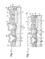
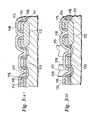
- In the prior art, as shown in Figs. 5(a) and 5(b), after
second underlayer wiring 73 is formed in asemiconductor substrate 71 which has first underlayer wiring (diffused layer) 72 formed by diffusing, alayer insulating film 74 of SiO2 or the like is deposited; and thereafter, acontact hole 74a is formed by etching or the like.Upper wiring 75 is formed over thecontact hole 74a; and thus, the wirings are electrically connected between the upper and lower layers. - In particular, in the case where the
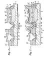
overlayer wiring 75 is made of a metal material like A1 while the first underlayer wiring 72 is formed of the diffused layer formed in thesubstrate 71, it is likely that themetal wiring 75 and thesubstrate 71 are short-circuited in a part shown by an arrow Q in Fig. 6 when thecontact hole 74a and the diffused layer, or thefirst underlayer wiring 72, are out of alignment. However, as shown in Fig. 7, such short-circuiting can be prevented if the surface of the substrate which is exposed because of the contact hole formed for the purpose of the connection with thefirst underlayer wiring 72 is covered with apolycrystalline Si film 76 doped with an impurity at high concentration so that thepolycrystalline Si film 76 is interposed between themetal wiring 75 and thesubstrate 71. Specifically, the short-circuiting between thesubstrate 71 and themetal wiring 75 is prevented by covering the end of the diffused region exposed in thecontact hole 74a with thepolycrystalline Si film 76 which is doped with an impurity at high concentration. This is because an impurity with which thepolycrystalline Si film 76 is doped at high concentration is diffused towards the substrate, so that no short-circuiting is caused even if thepolycrystalline Si film 76 is deposited on the end of the diffused region. - Two problems arise in the above-mentioned way of covering the
contact hole 74a with the the polycrystalline Si film 76: - For example, a case in which the
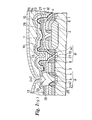
polycrystalline Si film 76 covering thesubstrate 71 in the contact holes is etched will be discussed. When thepolycrystalline Si film 76 is etched under the state where a part of the substrate is exposed because of the misregistration of the photoresist determining the configuration of thepolycrystalline Si film 76 to be etched, the exposed portion is etched away as shown by an arrow R in Fig. 8 because the substrate is of silicon. The etching of the substrate may cause drawbacks such as a junction leakage and the like. Hence, the end of thecontact hole 74a in thepolycrystalline Si film 76 must be positioned a distance d (0.1 µm to 0.3 µm) from the region where the substrate is exposed [see Fig. 11]. - On the other hand, the lowermost limit of the distance between polycrystalline Si patterns is determined by the resolution of a light exposing projector. Thus, the minimum distance between the contact holes is about double the distance d (0.2 µm to 0.6 µm) added to the resolution (about 0.6 µm) of the exposing projector. In other words, approximating a distance L between the
contact holes - As shown in Fig. 9, the
layer insulating film 74 is deposited on thesecond underlayer wiring 73, and then a portion where a contact hole is to be formed is etched down by the depth corresponding to the thickness of thelayer insulating film 74 to form the contact hole on the surface of the substrate in self-alignment relative to thesecond underlayer wiring 73. - However, when a plurality of overlayer wiring layers 75 exist to connect with the
substrate 71,layer insulating films substrate 71 as many times. If the plurality of layers are deposited in such a manner, the layer insulating film on the underlayer wiring is substantially thicker than the layer insulating film on the contact hole to fill the contact hole with the insulating film, so that it is impossible to form the contact holes in self-alignment. - The documents EP-A-0 337 436 and JP-A-62 86853 disclose semiconductor devices in which capacitors are formed in contact holes between gate portions on a substrate.
- To overcome the above-mentioned problems, the present invention is directed to a method of manufacturing a semiconductor memory in which a contact hole reliably making a contact with a diffused region of the semiconductor substrate can be formed while good yields of semiconductor memories can be attained even if the accuracy in the alignment of patterns in light projection and exposure is unsatisfactory.
- According to the present invention, there is provided a method of forming a contact opening to a predetermined region of a semiconductor substrate having underlayer wiring which is composed of a plurality of gate portions provided with side walls and a diffused region between the gate portions, said method comprising:
- i) forming over said region a first layer of an insulating material which is thinner in a direction perpendicular to the substrate than the side walls of each of the gate portions;
- ii) forming a conductive layer over said insulating layer,
- iii) removing portions of the conductive layer so that a portion having an upwardly extending side remains where said contact opening is to be formed,
- iv) forming a second layer of insulating material over the first layer and over said conductive layer portion so that an upwardly extending portion of the second insulating layer is formed on said upwardly extending side, and
- v) forming the contact opening through said second insulating layer, by removal of said conductive layer portion and etching the first insulating layer, such that the contact opening is formed in self-alignment relative to said underlayer wiring and the upwardly extending portion of the second insulating layer forms an upward projection at an upper part of the contact opening.
- Preferably, a further contact is formed to a further diffused region between the gate portions of the substrate, by the steps of:
- etching the first insulating layer to form a further contact hole extending to the further diffused region in self-alignment;
- depositing said conductive layer over the further contact hole;
- removing the conductive layer so that a further portion thereof remains where the further contact is to be formed in the further diffused region, so that the further contact hole is filled by the further portion;
- depositing said second insulating layer over the further
- portion such that the further portion becomes a buried layer and forming a through-hole to the buried layer through the second insulating layer.
- Preferably, the semiconductor substrate is a Si substrate, the first insulating layer is a SiO2 film, and the conductive layer is a polysilicon layer.
- Specific embodiments of the present invention will now be described with reference to the accompanying drawings, in which:-
- Fig. 1 is a diagram for explaining the steps of forming a capacitor electrode in a manufacturing method of an embodiment according to the present invention;
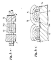
- Figs. 2(a) and 2(b) are diagrams for explaining a configuration of a main portion, showing a contact hole for making a contact with the capacitor electrode and a capacitor insulating film of the embodiment;
- Fig. 3 is a diagram for explaining the steps of forming a capacitor electrode in a manufacturing method of another embodiment according to the present invention;
- Fig. 4 is a diagram for explaining a configuration of a main portion, showing a memory formed in accordance with the embodiment;
- Fig. 5(a) is a diagram for explaining a configuration of a prior art semiconductor memory, showing a contact hole;
- Fig. 5(b) is a sectional view taken along the line A - A' of Fig. 5(a);
- Fig. 6 is a diagram for explaining drawbacks of the prior art semiconductor memory, showing its configuration;
- Fig. 7 is a diagram for explaining an improved prior art semiconductor memory, showing its configuration;
- Figs. 8 through 11 are diagrams for explaining drawbacks the improved prior art semiconductor memory, showing its configuration; and
- Fig. 12 is a diagram for explaining the accuracy of the alignment in an exposure device in the steps of forming a contact hole without a self-alignment method.
- The most significant characteristic of the present invention is that a contact hole extending to a diffused region in a memory cell is formed in self-alignment.
- In the present invention, first, on a semiconductor substrate a layer insulating film of a material which is more easily etched than the material of the semiconductor substrate is formed. For example, a SiO2 film is formed on a Si substrate.
- Then, a conductive layer of a material which is more easily etched than the material of the layer insulating film is deposited over the entire surface of the layer insulation film; and eventually, the conductive layer and layer insulating film in a portion where a contact hole is to be formed are removed by etching one after another to form the contact hole extending to the diffused region. In this way, the contact hole can be formed in self-alignment. The inventors of the present invention apply the above-mentioned method of forming a contact hole to the formation of a contact hole for forming a capacitor electrode of a memory cell to attain a high integration of a memory and good yields of memories.
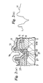
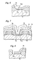
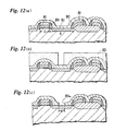
- An essential requirement in the present invention is that the insulating film layer is thinner than side walls of a gate portion. For example, an example is shown in Fig. 12 where a contact hole is formed in a layer insulating film without self-alignment as in the present invention.
- In Fig. 12(a), a layer
insulating film 82 is formed on a semiconductor substrate having underlayer wiring which is composed of a plurality ofgate portions 81 havingside walls 80 and a diffused region. In this case, the distance x between the gates is 1.1 - 1.2 µm while the length G of the gate is 0.8 µm or under, desirably 0.5 - 0.6 µm. - Then, as shown in Fig. 12(b), a
resist film 83 for forming a contact hole is formed. - Then, the layer insulating film is patterned by light projection and exposure, and reactive ion etching to form a
contact hole 83a. The diameter K of thecontact hole 83a is 0.3 µm. - In the above-mentioned method of forming a contact hole, it is known that the distance x between the gates cannot be reduced to 1.1 - 1.2 µm or under because of the accuracy of the alignment of the exposure device. Thus, it is necessary to arrange in advance that the adjacent gates are disposed with the distance x of 1.1 - 1.2 µm or over before the contact hole is formed. On the other hand, in the present invention, the distance x can be reduced to 0.5 - 0.6 µm. This results in high integration of the memory. For that purpose in the present invention, as shown in Fig. 1(b), a
conductive film 8 is formed for increasing in a margin of the alignment in forming a contact hole 40 [see Fig. 1(e)]. Theconductive film 8 also functions as a dummy, which is removed when the contact hole is formed. Thus, after the removal of theconductive film 8, a capacitor electrode can increase in area for wiring by an area the conductive film covers. - Since the
conductive film 8 is formed in forming thecontact hole 40 to increase in a margin of the alignment, the alignment of patterns in a projection and exposure may be performed with less accuracy; and therefore, good manufacturing yields can be expected. - The
contact hole 40 in the present invention is formed, for example, in the following way: A region R where a contact hole is to be formed is removed by an anisotropic reactive ion etching (RIE) with a mask of a resistpattern 50 formed by a projection and exposure, and then, a secondlayer insulating layer 9, theconductive film 8 and a firstlayer insulating film 27 are removed one after another by etching. The bottom face of thecontact hole 40, as shown in Fig. 1(e), defines ainterface 1a to the surface of one of diffused regions, while anupper opening 1b, or the rim, of thecontact hole 40 extends from a second insulatinglayer 29 to project upwards; a large level difference H between theupper opening 1b and thebottom face 1a is observed [see Fig. 1(e), Fig. 2]. Theconductive film 8 serving as a dummy [see Figs. 1(c) and 1(d)] is removed when thecontact hole 40 is formed; instead, an area for wiring can be accordingly increased in the depthwise direction. Thus, capacitor electrode overlayer wiring provided along the inner wall of the contact hole can increase its area of wiring. In other words, creating a large level difference in the contact portion between the capacitor electrode and the diffused region increases the area of the capacitor electrode. - Preferably, the conductive layer in the present invention may be the one that could be removed more rapidly than a SiO2 film by anisotropic etching like RIE; the best example is a polycrystalline silicon film. A silicide film of WSi or the like overlaid with a poly Si film may be used.
- The conductive layer is, for example, removed by anisotropic reactive ion etching (RIE) with a photoresist pattern formed by the projection and exposure, and a conductive film and a conductive buried film are formed.
- In another aspect of the present invention, a contact hole for connecting a bit line through its opening and a buried film to a diffused region can be formed in self-alignment. As a result, the cell can be miniaturized. In this case, the buried film is useful for increasing a margin of the alignment.
- In still another aspect of the present invention, a conductive film (e.g., a polysilicon film) which is etched more rapidly is deposited on a layer insulating film and patterned; thereafter, an insulating film is formed to form a contact hole. In this way, the contact hole can be assuredly formed in an area where the contact hole should be formed. The contact hole is filled with polycrystalline Si of high impurity concentration; and thus, when wiring formed by depositing conductive material on the semiconductor substrate is electrically connected to wiring formed by diffusion or the like in the semiconductor substrate, the wiring of the semiconductor substrate can be reliably drawn out on the semiconductor substrate. In this way, a memory with reliable connection of wiring can be created.
- The present invention will be explained below in detail in conjunction with embodiments shown in the drawings; it is not intended that the present invention be limited to the precise form disclosed therein but rather is defined by the appended claims.
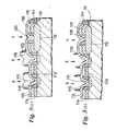
- Referring to Fig. 1(g), a DRAM (MOS transistor) is mainly composed of a Si substrate 1 of which elements are isolated by a SiO2 thermal oxidation film 2 having a thickness of approximately 0.4 µm, a polycrystalline Si film (gate wiring serving as lead) 4 formed on the substrate 1 with a thickness of about 300 nm (3000 Å) by diffusing phosphorus (P) at high concentration through a gate oxidation film 3 having a thickness of about 10nm (100 Å), SiO2 spacers 5 and 6 formed by anisotropic ion reactive etching (RIE) after a deposition of SiO2 on the upper and side faces of the gate wiring by CVD, a layer insulating SiO2 film 27 formed by CVD to cover it and to have a thickness of about 0.2 µm, a contact hole 40 formed on one of diffused regions, R, with a large level difference H of about 1.2 µm between the upper opening 1b and the bottom face 1a [see Fig. 1(e)], a bit line connecting contact-hole 242 formed on the other of the diffused regions, K, through the polycrystalline Si film 28 having a thickness of about 0.5 µm, an SiO2 film 29 deposited on the Si substrate by CVD with a thickness of about 0.1 µm and a capacitor electrode overlayer wiring 41 provided with the contact hole interposed, both of which are provided on a region except the diffused region K, a SiO2 film 13 formed by CVD with a thickness of about 0.1 µm and a fourth layer insulating film 14 formed by CVD with a thickness of about 0.3 µm for flattening, both of which are deposited on the SiO2 film 29 one after another, and overlayer bit-wiring 15 formed by light projection and exposure and anisotropic RIE after a deposition of a WSi film of about 0.3 µm thickness on the SiO2 film 14 including an opening 242 above a contact hole 42.
- The
capacitor electrode 41 is composed of a capacitorlower electrode 10 which is formed in the lower layer by depositing a polycrystalline Si of about 50nm (500 Å) thickness film doped with phosphorus (P) at high concentration by CVD and patterning it by light projection and exposure, and anisotropic RIE, and a capacitorupper electrode 12 which is formed in the upper layer through a SiNcapacitor insulating film 11 of about 8nm (80 Å) thickness by light projection and exposure, and anisotropic RIE after a deposition of a polycrystalline Si film dcped with P at high concentration of about 150 nm (1500 Å) thickness. - Then, manufacturing methods will be explained.
- (i) First, all over the
Si substrate 1 which includes agate electrode 4 having theupper side 5 of the spacer of SiO2 and the side face (side wall) 6 of the spacer of SiO2, a SiO2 film serving as an insulating layer and a resist layer (not shown) are deposited one after another [see Fig. 1(a)], and a resist film of a specific pattern is formed; thereafter, - (ii) with a mask of the resist film, only the portion of the SiO2 film 27 on the diffused region K is removed by anisotropic RIE until the surface lllb of the diffused region K is partly exposed. After that, all over the
Si substrate 1 including the remaining SiO2 film 27, a polycrystalline Si layer (not shown) serving as a conductive layer of a material etched more rapidly than the SiO2 film 27 and a resist layer (not shown) are deposited one after another, and a resist film of a specific pattern is formed; thereafter, - (iii) with a mask of the resist film, the conductive layer is etched so that the
conductive film 8 remains through the SiO2 film 27 on the diffused region R while the conductive buriedfilm 28 electrically connecting to the diffused region K remains on the diffused region K [see Fig. 1(b)]. - (iv) All over the first
layer insulating film 27 including theconductive film 8 and the conductive buriedfilm 28, a SiO2 film 9 and a resist layer (not shown) are deposited one after another [see Fig. 1(c)], and a resistfilm 50 of a specific pattern for forming a contact hole is formed [see Fig. 1(d)]; thereafter, - (v) with a mask of the resist
film 50, the SiO2 film 9 andconductive film 8 on the diffused region R are etched one after another, and further, the SiO2 film 27 just under theconductive film 8 is removed until it is partly exposed on the interface la to thesubstrate 1 in the diffused region R to form thecontact hole 40 and the SiO2 film 29 [see Fig. 1(e)]. - (vi) Then, on the
Si substrate 1 except the diffused region region K or other, thecapacitor 41 is formed [see Fig. 1(f)]. - The
capacitor 41 is composed of a capacitorlower electrode 10 which is formed in the lower layer by depositing a polycrystalline Si of about 50nm (500 Å) thickness film doped with phosphorus (P) at high concentration by CVD and patterning it by light projection and exposure, and anisotropic RIE, and a capacitorupper electrode 12 which is formed in the upper layer through a SiNcapacitor insulating film 11 of about 8nm (80 Å) thickness by light projection and exposure, and anisotropic RIE after a deposition of a polycrystalline Si film doped with P at high concentration of about 150nm (1500 Å) thickness. Thus, thecontact hole 40 is filled with the capacitorupper electrode 12 and the capacitorlower electrode 10. - (vii) Moreover, all over the
Si substrate 1 including thecapacitor 41, the SiO2 film 13 and the SiO2 film 14 for flattening are deposited one after another, and then, the SiO2 films 13, 14 on the conductive buriedfilm 28 are removed to form a contact hole (bit line contact hole) 242. - (viii) All over the SiO2 film 14 including the contact hole, the bit line 15 of a specific pattern is formed [see Fig. 1(g)].
- In this way, a DRAM memory cell is configured.
- In this embodiment, after the
word line 4 is formed, thepoly Si patterns conductive film 8 as a dummy in the poly Si patterns are removed by etching, and then, thecapacitor 41 is formed. As a result, thecapacitor 41 increases in its electrode area. As the area of the capacitor electrodes increases, the amount of electric charge accumulated at the identical writing voltage is increased; and the reliability against a soft error caused by an incident of α particle is enhanced. - The contact holes 40, 42 are formed on both the diffused layers by providing the
poly Si patterns - As has been described, according to the present invention; (i) good yields in manufacturing can be expected because the alignment of the patterns in a projection and exposure can be performed with less accuracy, and (ii) the area of the capacitor electrodes can be increased by using a level difference between the contact portions in the capacitor electrode and the diffused layer. Because of an increase in the area of the capacitor electrodes, the resultant amount of accumulated electric charge can be increased under the identical writing voltage, and the reliability against a soft error can be enhanced.
- In Fig. 3(a), a thermally oxidized
gate insulating film 113 of about 10nm (100 Å) thickness is formed on asemiconductor substrate 111 of which elements are isolated by athermal oxidation film 112 of about 0.4 µm, and gate wiring of a MOS transistor andsecond underlayer wiring 114 are formed on thegate insulating film 113 with a polycrystalline Si film of about 30nm (3000 Å) thickness diffused with phosphorus at high concentration. On the upper and side faces of thewiring 114,spacers first underlayer wiring 117 is formed in thesubstrate 111 by a diffusion with masks of thespacers spacers spacers - As shown in Fig. 3(b), a
polycrystalline Si film 119 of about 0.5 µm thickness which is different in a period of time required for etching from SiO2 is deposited on the substrate, covering the SiO2 film 118, and then etched by an anisotropic etching, such as RIE or the like, with a photoresist pattern formed by light projection and exposure, so as to form a dummy pattern in a portion X where a contact hole is necessary. A region between the wirings where no contact hole is necessary in this process has the insulatingfilm 118 shown by reference character Y in Fig. 3(c). - After that, a thin SiO2 film 120 of about 0.1 µm thickness is deposited by CVD, and then, the surface of the substrate is etched back by an anisotropic etching, such as RIE or the like, to the depth corresponding to the thickness of the SiO2 film 120, as shown in Fig. 3(c). Then, the exposed
polycrystalline Si film 119 is removed by an isotropic etching, such as plasma etching or the like [see Fig. 3(d)]. Moreover, the SiO2 film 118 covering the surface of the substrate is etched back by an anisotropic etching, such as RIE or the like, to the depth corresponding to the thickness of the SiO2 film 118. With these steps, thesubstrate 111 is exposed in the portion X where the contact hole making a contact with the overlayer wiring is to be formed without losing the insulating film in the portion Y where no contact hole is necessary, and the contact hole is formed in self-alignment relative to a diffusedregion 117. - After that, a
polycrystalline Si film 121 of about 0.4 µm thickness which is doped with phosphorus at high concentration is deposited by CVD as shown in Fig. 3(e), and then etched back by an anisotropic etching, such as RIE or the like, to the depth corresponding to the thickness of thepolycrystalline Si film 121, so as to complete thepolycrystalline Si film 121 with which the contact hole is filled, as shown in Fig. 3 (f). After etching back thepolycrystalline Si film 121, a SiO2 film 122 of about 0.2 µm thickness is formed on the surface of the substrate by CVD. - With the above-mentioned steps, the polycrystalline Si buried
layer 121 covering the contact hole on the diffused region is formed in self-alignment. The pattern of thepolycrystalline Si film 121 is simultaneously formed in every portion where the contact hole making a contact between the multi-layer overlayer wiring and the substrate is to be formed, so that the polycrystalline Si buried layer is formed in every contact hole in self-alignment relative to the second underlayer wiring. The buriedlayer 121 close to the substrate is directly in contact with the diffusedregion 117 on the surface of the substrate to attain an electrical connection. - After the buried
layer 121 is formed, a semiconductor device having a capacitor and bit line, which are essential for forming a memory cell, formed in a multi-layer wiring configuration on the semiconductor substrate, as shown in Fig. 4. - To form the capacitor, a thin CVD SiO2 film 122 which covers a buried
layer 121b to connect with the capacitor is removed, and then a capacitorlower electrode 131 connected to the buriedlayer 121b in the portion from which the SiO2 film 122 was removed is formed. Then, acapacitor insulating film 132 is formed, covering thelower electrode 131; moreover, a capacitorupper electrode 133 is deposited. - With the above-mentioned deposition step, an insulating material is formed as an insulating
film layer 134 on the surface of the semiconductor substrate in which memory cell capacitor elements are formed, and bitline 136 is formed through the insulatingfilm 134. Thebit line 136 is formed of a multi-layer conductor ofpolycrystalline Si wiring 136a and a metal having a high fusing point and is connected to the buriedpolycrystalline Si film 121a in a portion where the connection to the wiring formed in the semiconductor substrate is necessary. In the connection process, since the wiring formed in the substrate by diffusion has been drawn out on the substrate by the buriedlayer 121a, a sufficient contact area can be retained for an assured electrical connection. - Multi-layer wiring including four layers or over is employed in a high integrated LSI of 0.6 µm wiring width, such as a 16 MDRAM and the like, and the wiring to be connected to the substrate also includes two layers or over. In such a semiconductor configuration, also, the pattern of the
polycrystalline Si film 121 is simultaneously formed in every portion where the contact hole making a contact between the multi-layer overlayer wiring and the substrate is to be formed, so that the polycrystalline Si buried layer is formed in every contact hole in self-alignment relative to the gate wiring. - The semiconductor device shown in Fig. 4 has a configuration having underlayer wiring which is a diffused layer formed in the substrate, and overlayer wiring which consists of a capacitor lower electrode of a memory cell and a bit line.
- As previously mentioned, according to the present invention, a contact hole which makes a contact between multi-layer underlayer and overlayer wirings in a high integrated LSI having a wiring width of 0.6 µm or under can be reliably formed at high density. The contact hole between the underlayer and overlayer wirings is formed in self-alignment relative to the wirings, so that the alignment of the patterns in a projection and exposure can be performed with less accuracy. Thus, good yields in manufacturing can be expected. The present invention is suitable especially for a semiconductor memory which requires multi-layer wiring.
Claims (9)
- A method of forming a contact opening to a predetermined region (R) of a semiconductor substrate (1; 111) having underlayer wiring which is composed of a plurality of gate portions (4; 114) provided with side walls (6; 116) and a diffused region (R; 117) between the gate portions, said method comprising:i) forming over said region a first layer of an insulating material (7; 118) which is thinner in a direction perpendicular to the substrate than the side walls of each of the gate portions;characterised by the steps of:ii) forming a conductive layer over said insulating layer,iii) removing portions of the conductive layer so that a portion (8; 119) having an upwardly extending side remains where said contact opening is to be formed,iv) forming a second layer (9; 120) of insulating material over the first layer and over said conductive layer portion (8;119) so that an upwardly extending portion of the second insulating layer (9; 120) is formed on said upwardly extending side, andv) forming the contact opening (40) through said second insulating layer, by removal of said conductive layer portion (8;119) and etching the first insulating layer, such that the contact opening (40) is formed in self-alignment relative to said underlayer wiring and the upwardly extending portion of the second insulating layer (9; 120) forms an upward projection (120) at an upper part (16) of the contact opening (40).
- A method according to claim 1, wherein the step of forming the contact opening comprises forming a pattern film (50) over the second insulating layer (9) so as to cover said upwardly extending portion of the second insulating layer (9), and etching the second insulating layer (9) and the remaining portion (8) of the conductive layer so as to form said upward projection.
- A method according to claim 1 or claim 2, further comprising:
depositing a polysilicon layer (121) doped with impurity at high concentration over the contact opening and then etching back the polysilicon layer to form in the contact opening a buried layer of polysilicon (121a; 121b). - A method according to claim 3, further comprising forming overlayer wiring in contact with said buried polysilicon layer (121a).
- A method of forming a capacitor on a substrate, comprising forming a contact opening as claimed in any one of claims 1 to 3, and further including the steps of:i) depositing a polysilicon film doped with impurity at high concentration and patterning the polysilicon film by projection, exposure and reactive ion etching to form a capacitor lower electrode (10; 131) over said upward projection (120);ii) depositing a capacitor insulating film (11; 132); andiii) depositing a further polysilicon film doped with impurity at high concentration and patterning the further polysilicon film by projection, exposure and reactive ion etching to form a capacitor upper electrode (12; 133) opposing said lower electrode (10; 131).
- A method according to claim 5, wherein said polysilicon film forming said capacitor lower electrode (10) is deposited so as to cover the contact opening (40) and upward projection.
- A method according to any preceding claim, wherein the semiconductor substrate (1; 111) is a Si substrate, the first insulating layer (7; 118) is a SiO2 film and the conductive layer comprises polysilicon.
- A method as claimed in any preceding claim, further comprising forming a further contact to a further diffused region (K) between the gate portions of the substrate (1), by the steps of:etching the first insulating layer (7) to form a further contact hole (111b) extending to the further diffused region (K) in self-alignment;depositing said conductive layer over the further contact hole (111b);removing the conductive layer so that a further portion (28) thereof remains where the further contact is to be formed in the further diffused region, so that the further contact hole (111b) is filled by the further portion (28);depositing said second insulating layer (9) over the further portion (28) such that the further portion becomes a buried layer and forming a through-hole (242) to the buried layer through the second insulating layer (9).
- A method as claimed in claim 8, further comprising forming a bit line (15) connected to the buried layer (28) through the through-hole (242).
Applications Claiming Priority (4)
| Application Number | Priority Date | Filing Date | Title |
|---|---|---|---|
| JP340159/89 | 1989-12-29 | ||
| JP1340159A JP2574910B2 (en) | 1989-12-29 | 1989-12-29 | Method for manufacturing semiconductor device |
| JP2074639A JP2547882B2 (en) | 1990-03-23 | 1990-03-23 | Method for manufacturing semiconductor device |
| JP74639/90 | 1990-03-23 |
Publications (3)
| Publication Number | Publication Date |
|---|---|
| EP0439965A2 EP0439965A2 (en) | 1991-08-07 |
| EP0439965A3 EP0439965A3 (en) | 1991-12-04 |
| EP0439965B1 true EP0439965B1 (en) | 1997-04-09 |
Family
ID=26415810
Family Applications (1)
| Application Number | Title | Priority Date | Filing Date |
|---|---|---|---|
| EP90314415A Expired - Lifetime EP0439965B1 (en) | 1989-12-29 | 1990-12-28 | Method of manufacturing a semiconductor memory |
Country Status (5)
| Country | Link |
|---|---|
| US (2) | US5118640A (en) |
| EP (1) | EP0439965B1 (en) |
| KR (1) | KR960002078B1 (en) |
| DE (1) | DE69030433T2 (en) |
| TW (1) | TW218933B (en) |
Families Citing this family (13)
| Publication number | Priority date | Publication date | Assignee | Title |
|---|---|---|---|---|
| DE59009067D1 (en) * | 1990-04-27 | 1995-06-14 | Siemens Ag | Method for producing an opening in a semiconductor layer structure and its use for producing contact holes. |
| JP2524863B2 (en) * | 1990-05-02 | 1996-08-14 | 三菱電機株式会社 | Semiconductor device and manufacturing method thereof |
| US5236860A (en) * | 1991-01-04 | 1993-08-17 | Micron Technology, Inc. | Lateral extension stacked capacitor |
| US5231043A (en) * | 1991-08-21 | 1993-07-27 | Sgs-Thomson Microelectronics, Inc. | Contact alignment for integrated circuits |
| TW243541B (en) * | 1991-08-31 | 1995-03-21 | Samsung Electronics Co Ltd | |
| KR960003773B1 (en) * | 1992-08-25 | 1996-03-22 | 금성일렉트론주식회사 | Manufacture of dram cell |
| US5563089A (en) * | 1994-07-20 | 1996-10-08 | Micron Technology, Inc. | Method of forming a bit line over capacitor array of memory cells and an array of bit line over capacitor array of memory cells |
| US5605857A (en) * | 1993-02-12 | 1997-02-25 | Micron Technology, Inc. | Method of forming a bit line over capacitor array of memory cells and an array of bit line over capacitor array of memory cells |
| US5840605A (en) * | 1993-04-19 | 1998-11-24 | Industrial Technology Research Institute | Dual layer polysilicon capacitor node DRAM process |
| KR100388519B1 (en) * | 1995-02-22 | 2003-09-19 | 마이크론 테크놀로지, 인크. | Method for forming a bit line on a capacitor array of a memory cell and an integrated circuit and a semiconductor memory device using the same |
| WO2001009946A1 (en) * | 1999-07-29 | 2001-02-08 | Infineon Technologies Ag | Method for producing integrated semiconductor components |
| DE10332600B3 (en) | 2003-07-17 | 2005-04-14 | Infineon Technologies Ag | Method for producing an electrically conductive contact |
| JP4301227B2 (en) * | 2005-09-15 | 2009-07-22 | セイコーエプソン株式会社 | Electro-optical device and manufacturing method thereof, electronic apparatus, and condenser |
Family Cites Families (23)
| Publication number | Priority date | Publication date | Assignee | Title |
|---|---|---|---|---|
| US3986903A (en) * | 1974-03-13 | 1976-10-19 | Intel Corporation | Mosfet transistor and method of fabrication |
| US3984822A (en) * | 1974-12-30 | 1976-10-05 | Intel Corporation | Double polycrystalline silicon gate memory device |
| US4268951A (en) * | 1978-11-13 | 1981-05-26 | Rockwell International Corporation | Submicron semiconductor devices |
| JPS5681968A (en) * | 1979-12-07 | 1981-07-04 | Toshiba Corp | Manufacture of semiconductor device |
| US4577392A (en) * | 1984-08-03 | 1986-03-25 | Advanced Micro Devices, Inc. | Fabrication technique for integrated circuits |
| JPS6237960A (en) * | 1985-08-13 | 1987-02-18 | Toshiba Corp | Manufacture of read only semiconductor memory device |
| JPS6286853A (en) * | 1985-10-14 | 1987-04-21 | Fujitsu Ltd | Manufacture of semiconductor device |
| DE3609274A1 (en) * | 1986-03-19 | 1987-09-24 | Siemens Ag | METHOD FOR PRODUCING A SELF-ADJUSTED METAL CONTACT |
| JPS63237551A (en) * | 1987-03-26 | 1988-10-04 | Toshiba Corp | Manufacture of semiconductor device |
| US4916083A (en) * | 1987-05-11 | 1990-04-10 | International Business Machines Corporation | High performance sidewall emitter transistor |
| JPS63281457A (en) * | 1987-05-13 | 1988-11-17 | Hitachi Ltd | Semiconductor memory |
| JPH0834311B2 (en) * | 1987-06-10 | 1996-03-29 | 日本電装株式会社 | Method for manufacturing semiconductor device |
| JP2612836B2 (en) * | 1987-09-23 | 1997-05-21 | シーメンス、アクチエンゲゼルシヤフト | Method of manufacturing MESFET having self-aligned gate |
| US4852062A (en) * | 1987-09-28 | 1989-07-25 | Motorola, Inc. | EPROM device using asymmetrical transistor characteristics |
| JPH01129440A (en) * | 1987-11-14 | 1989-05-22 | Fujitsu Ltd | Semiconductor device |
| US4977105A (en) * | 1988-03-15 | 1990-12-11 | Mitsubishi Denki Kabushiki Kaisha | Method for manufacturing interconnection structure in semiconductor device |
| JP2723530B2 (en) * | 1988-04-13 | 1998-03-09 | 日本電気株式会社 | Method for manufacturing dynamic random access memory device |
| JP2695185B2 (en) * | 1988-05-02 | 1997-12-24 | 株式会社日立製作所 | Semiconductor integrated circuit device and method of manufacturing the same |
| KR900019227A (en) * | 1988-05-18 | 1990-12-24 | 아오이 죠이치 | Semiconductor memory device with stacked capacitor and manufacturing method thereof |
| JPH0278270A (en) * | 1988-09-14 | 1990-03-19 | Hitachi Ltd | Semiconductor memory device and manufacture thereof |
| JP2633650B2 (en) * | 1988-09-30 | 1997-07-23 | 株式会社東芝 | Semiconductor memory device and method of manufacturing the same |
| JP2904533B2 (en) * | 1989-03-09 | 1999-06-14 | 株式会社東芝 | Method for manufacturing semiconductor device |
| US4965217A (en) * | 1989-04-13 | 1990-10-23 | International Business Machines Corporation | Method of making a lateral transistor |
-
1990
- 1990-12-28 EP EP90314415A patent/EP0439965B1/en not_active Expired - Lifetime
- 1990-12-28 DE DE69030433T patent/DE69030433T2/en not_active Expired - Fee Related
- 1990-12-28 KR KR1019900022098A patent/KR960002078B1/en not_active IP Right Cessation
-
1991
- 1991-07-08 US US07/725,326 patent/US5118640A/en not_active Expired - Lifetime
- 1991-07-08 US US07/728,024 patent/US5100828A/en not_active Expired - Lifetime
-
1993
- 1993-02-04 TW TW079110800A01A patent/TW218933B/zh active
Non-Patent Citations (1)
| Title |
|---|
| PATENT ABSTRACTS OF JAPAN, vol.14, no. 292 (E-944)(4235), 25th June 1990; & JP-A-2 094 554 * |
Also Published As
| Publication number | Publication date |
|---|---|
| KR910013505A (en) | 1991-08-08 |
| DE69030433D1 (en) | 1997-05-15 |
| KR960002078B1 (en) | 1996-02-10 |
| DE69030433T2 (en) | 1997-10-09 |
| EP0439965A2 (en) | 1991-08-07 |
| US5100828A (en) | 1992-03-31 |
| TW218933B (en) | 1994-01-11 |
| EP0439965A3 (en) | 1991-12-04 |
| US5118640A (en) | 1992-06-02 |
Similar Documents
| Publication | Publication Date | Title |
|---|---|---|
| US4849854A (en) | Semiconductor device and method of manufacturing the same | |
| EP0348046B1 (en) | Method of producing a semiconductor device | |
| EP0299505B1 (en) | Semiconductor device and manufacturing method thereof | |
| EP0503205B1 (en) | EPROM and method of producing same | |
| JP3116360B2 (en) | Method for forming self-aligned contact hole and semiconductor device | |
| EP0439965B1 (en) | Method of manufacturing a semiconductor memory | |
| KR100188822B1 (en) | Dynamic random access memory device having reduced stepped portions | |
| US5834816A (en) | MOSFET having tapered gate electrode | |
| US5247197A (en) | Dynamic random access memory device having improved contact hole structures | |
| US5792704A (en) | Method for fabricating wiring in semiconductor device | |
| US4504333A (en) | Method of making field oxide regions | |
| JPH0817943A (en) | Manufacture of semiconductor device | |
| KR100285698B1 (en) | Manufacturing method of semiconductor device | |
| JP3190659B2 (en) | Semiconductor memory and manufacturing method thereof | |
| US5920124A (en) | Semiconductor device having misalignment resistive interconnect layers | |
| EP0315421B1 (en) | Semiconductor integrated circuit device having at least two contact holes | |
| KR20020074551A (en) | Method of forming a metal line in a semiconductor device | |
| JP3209639B2 (en) | Method for manufacturing semiconductor device | |
| US5160988A (en) | Semiconductor device with composite surface insulator | |
| JP3592870B2 (en) | Method for manufacturing semiconductor device | |
| JP2547882B2 (en) | Method for manufacturing semiconductor device | |
| JP2855981B2 (en) | Method for manufacturing semiconductor device | |
| JP3355613B2 (en) | Semiconductor memory device and method of manufacturing the same | |
| JP2574910B2 (en) | Method for manufacturing semiconductor device | |
| JP2876670B2 (en) | Manufacturing method of nonvolatile semiconductor memory device |
Legal Events
| Date | Code | Title | Description |
|---|---|---|---|
| PUAI | Public reference made under article 153(3) epc to a published international application that has entered the european phase |
Free format text: ORIGINAL CODE: 0009012 |
|
| 17P | Request for examination filed |
Effective date: 19910102 |
|
| AK | Designated contracting states |
Kind code of ref document: A2 Designated state(s): DE FR GB IT NL |
|
| PUAL | Search report despatched |
Free format text: ORIGINAL CODE: 0009013 |
|
| AK | Designated contracting states |
Kind code of ref document: A3 Designated state(s): DE FR GB IT NL |
|
| 17Q | First examination report despatched |
Effective date: 19940503 |
|
| GRAG | Despatch of communication of intention to grant |
Free format text: ORIGINAL CODE: EPIDOS AGRA |
|
| GRAH | Despatch of communication of intention to grant a patent |
Free format text: ORIGINAL CODE: EPIDOS IGRA |
|
| GRAH | Despatch of communication of intention to grant a patent |
Free format text: ORIGINAL CODE: EPIDOS IGRA |
|
| GRAA | (expected) grant |
Free format text: ORIGINAL CODE: 0009210 |
|
| AK | Designated contracting states |
Kind code of ref document: B1 Designated state(s): DE FR GB IT NL |
|
| ITF | It: translation for a ep patent filed |
Owner name: 0508;09MIFRACHELI & C. S.R.L. |
|
| REF | Corresponds to: |
Ref document number: 69030433 Country of ref document: DE Date of ref document: 19970515 |
|
| ET | Fr: translation filed | ||
| PLBE | No opposition filed within time limit |
Free format text: ORIGINAL CODE: 0009261 |
|
| STAA | Information on the status of an ep patent application or granted ep patent |
Free format text: STATUS: NO OPPOSITION FILED WITHIN TIME LIMIT |
|
| 26N | No opposition filed | ||
| REG | Reference to a national code |
Ref country code: GB Ref legal event code: IF02 |
|
| PGFP | Annual fee paid to national office [announced via postgrant information from national office to epo] |
Ref country code: NL Payment date: 20081215 Year of fee payment: 19 |
|
| PGFP | Annual fee paid to national office [announced via postgrant information from national office to epo] |
Ref country code: FR Payment date: 20081212 Year of fee payment: 19 |
|
| PGFP | Annual fee paid to national office [announced via postgrant information from national office to epo] |
Ref country code: DE Payment date: 20081229 Year of fee payment: 19 |
|
| PGFP | Annual fee paid to national office [announced via postgrant information from national office to epo] |
Ref country code: GB Payment date: 20081224 Year of fee payment: 19 |
|
| PGFP | Annual fee paid to national office [announced via postgrant information from national office to epo] |
Ref country code: IT Payment date: 20081229 Year of fee payment: 19 |
|
| REG | Reference to a national code |
Ref country code: NL Ref legal event code: V1 Effective date: 20100701 |
|
| GBPC | Gb: european patent ceased through non-payment of renewal fee |
Effective date: 20091228 |
|
| REG | Reference to a national code |
Ref country code: FR Ref legal event code: ST Effective date: 20100831 |
|
| PG25 | Lapsed in a contracting state [announced via postgrant information from national office to epo] |
Ref country code: FR Free format text: LAPSE BECAUSE OF NON-PAYMENT OF DUE FEES Effective date: 20091231 Ref country code: NL Free format text: LAPSE BECAUSE OF NON-PAYMENT OF DUE FEES Effective date: 20100701 |
|
| PG25 | Lapsed in a contracting state [announced via postgrant information from national office to epo] |
Ref country code: DE Free format text: LAPSE BECAUSE OF NON-PAYMENT OF DUE FEES Effective date: 20100701 |
|
| PG25 | Lapsed in a contracting state [announced via postgrant information from national office to epo] |
Ref country code: GB Free format text: LAPSE BECAUSE OF NON-PAYMENT OF DUE FEES Effective date: 20091228 |
|
| PG25 | Lapsed in a contracting state [announced via postgrant information from national office to epo] |
Ref country code: IT Free format text: LAPSE BECAUSE OF NON-PAYMENT OF DUE FEES Effective date: 20091228 |