EP0439322A2 - Verfahren und Vorrichtung zur Messung des Spaltes zwischen zwei einander gegenüberliegenden Objekten - Google Patents
Verfahren und Vorrichtung zur Messung des Spaltes zwischen zwei einander gegenüberliegenden Objekten Download PDFInfo
- Publication number
- EP0439322A2 EP0439322A2 EP91300463A EP91300463A EP0439322A2 EP 0439322 A2 EP0439322 A2 EP 0439322A2 EP 91300463 A EP91300463 A EP 91300463A EP 91300463 A EP91300463 A EP 91300463A EP 0439322 A2 EP0439322 A2 EP 0439322A2
- Authority
- EP
- European Patent Office
- Prior art keywords
- wafer
- mask
- grating
- reflected
- light
- Prior art date
- Legal status (The legal status is an assumption and is not a legal conclusion. Google has not performed a legal analysis and makes no representation as to the accuracy of the status listed.)
- Granted
Links
Images




Classifications
-
- G—PHYSICS
- G03—PHOTOGRAPHY; CINEMATOGRAPHY; ANALOGOUS TECHNIQUES USING WAVES OTHER THAN OPTICAL WAVES; ELECTROGRAPHY; HOLOGRAPHY
- G03F—PHOTOMECHANICAL PRODUCTION OF TEXTURED OR PATTERNED SURFACES, e.g. FOR PRINTING, FOR PROCESSING OF SEMICONDUCTOR DEVICES; MATERIALS THEREFOR; ORIGINALS THEREFOR; APPARATUS SPECIALLY ADAPTED THEREFOR
- G03F9/00—Registration or positioning of originals, masks, frames, photographic sheets or textured or patterned surfaces, e.g. automatically
- G03F9/70—Registration or positioning of originals, masks, frames, photographic sheets or textured or patterned surfaces, e.g. automatically for microlithography
- G03F9/7073—Alignment marks and their environment
- G03F9/7076—Mark details, e.g. phase grating mark, temporary mark
-
- G—PHYSICS
- G03—PHOTOGRAPHY; CINEMATOGRAPHY; ANALOGOUS TECHNIQUES USING WAVES OTHER THAN OPTICAL WAVES; ELECTROGRAPHY; HOLOGRAPHY
- G03F—PHOTOMECHANICAL PRODUCTION OF TEXTURED OR PATTERNED SURFACES, e.g. FOR PRINTING, FOR PROCESSING OF SEMICONDUCTOR DEVICES; MATERIALS THEREFOR; ORIGINALS THEREFOR; APPARATUS SPECIALLY ADAPTED THEREFOR
- G03F9/00—Registration or positioning of originals, masks, frames, photographic sheets or textured or patterned surfaces, e.g. automatically
- G03F9/70—Registration or positioning of originals, masks, frames, photographic sheets or textured or patterned surfaces, e.g. automatically for microlithography
- G03F9/7003—Alignment type or strategy, e.g. leveling, global alignment
- G03F9/7023—Aligning or positioning in direction perpendicular to substrate surface
Definitions
- This invention relates to a deviation measuring device for measuring the interval between two objects at high precision.
- the invention is suitably usable in a semiconductor device manufacturing apparatus, for controlling the interval between a mask and a wafer to a predetermined magnitude.
- the interval between a mask and a wafer is measured by using an interval measuring device and, after the interval is controlled to a predetermined magnitude, a pattern of the mask is photolithographically transferred to the wafer.
- Figure 7 is a schematic representation of an interval measuring device as proposed in Japanese Laid-Open Patent Application No. Sho 61-111402. As illustrated, a mask (first object) M and a wafer (second object) W are disposed opposed to each other, and light is projected and focused by a lens L1 at a point PS between the mask M and the wafer W.
- the light is reflected by the surface of the mask M and the surface of the wafer W, sequentially, and beams of reflected light from the mask M and the wafer W are projected and focused by another lens L2 at points PW and PM on a screen S surface.
- the interval between the mask M and the wafer W can be measured by detecting the spacing between the spots PW and PM of focused light on the screen S surface.
- a device for detecting relative positional deviation between a mask and a wafer wherein the mask has a first grating pattern and a zone plate pattern and the wafer has a second grating pattern
- said device comprising: directing means for directing a radiation beam to the first grating pattern of the mask, such that the first grating pattern produces a first transmitted beam which is then inputted to the wafer substantially perpendicularly and a second transmitted beam which is obliquely inputted to the wafer and such that the first grating pattern also produces a first reflected beam; and detecting means for detecting (i) the first reflected beam and also for detecting (ii) a second reflected beam resulting from reflective diffraction of the first transmitted beam by the second diffraction pattern of the wafer and being displaceable with any inclination of a surface of the wafer and (iii) a third reflected beam resulting from reflection of the
- a device for detecting a relative positional deviation between a mask and a wafer wherein the mask has first and second grating patterns and a zone plate pattern disposed with a predetermined orientation together with the second grating pattern, wherein the wafer has a third grating pattern, and wherein each of the first to third grating patterns is provided by grating elements of regular intervals, said device comprising: directing means for directing a radiation beam to the first and second grating patters of the mask so that it is obliquely inputted to the mask with respect to a plane substantially orthogonal to said predetermined direction, such that the first grating pattern produces a first transmissively diffracted beam which is then inputted to the wafer substantially perpendicularly and also produces a first reflected beam while the second grating pattern produces a second transmissively diffracted beam which is then obliquely inputted to the wafer; and photodetecting means having a
- a device for detecting a relative positional deviation between a mask and a wafer comprising: directing means for directing a radiation beam to the mask, such that the mask produces a first transmitted beam which is then inputted to the wafer substantially perpendicularly and a second transmitted beam which is then obliquely inputted to the wafer and that the mask also produces a first reflected beam; and detecting means for detecting (i) the first reflected beam and also for detecting (ii) a second reflected beam resulting from reflection of the first transmitted beam by the wafer and (iii) a third reflected beam resulting from reflection of the second transmitted beam by the wafer and from diffraction of the same by a zone plate of the mask and being displaceable with any inclination of the wafer and with an interval between the mask and the wafer.
- the detecting means comprises photoelectric converting means for detecting positions of incidence of the first, second and third reflected beams thereupon.
- the photoelectric converting means may comprise an array of first, second and third photodetectors for receiving the first, second and third reflected beams independently of each other.
- it may comprise a single photodetector such as, for example, an image pickup device having light receiving elements arrayed two-dimensionally.
- This photodetector may comprise arrayed light receiving elements, or a position sensitive detector may be used.
- a single light collecting lens system may be used to direct the first, second and third reflected beams to the photoelectric converting means, or separate, first, second and third light collecting lens systems may be used to direct the first to third reflected beams to the photoelectric converting means independently of each other.
- first, second and third light collecting lens systems may be used to direct the first to third reflected beams to the photoelectric converting means independently of each other.
- the present invention is attainable without such a lens system or systems.
- the directing means may comprise a light emitting diode (LED) or a semiconductor laser, which emits the radiation beam.
- LED light emitting diode
- the directing means may direct a substantially parallel light beam to the first grating pattern.
- each grating pattern may be provided by grating elements of regular intervals, having substantially no power.
- the photoelectric converting means is structured so as to be responsive to displacement of the first, second or third reflected beam in a predetermined direction, and the grating lines of each grating pattern extend obliquely to that direction.
- the directing means and the detecting means or the photoelectric converting means may be mounted to an optical detection head which may be made movable along the surface of the mask.
- any inclination of the wafer surface with respect to a predetermined plane may be detected and then corrected while, on the other hand, the interval between the mask and the wafer may be determined on the basis of the position of incidence of the first reflected beam upon the photoelectric converting means and the position of incidence of the third reflected beam upon the photoelectric converting means.
- the present invention is particularly suitably applicable to an exposure apparatus for manufacture of semiconductor devices. More particularly, the invention is suitably usable in a proximity type exposure apparatus wherein a mask and a wafer are placed close to each other.
- Figure 1 is a perspective view, schematically illustrating a major portion of a deviation measuring device according to an embodiment of the present invention.
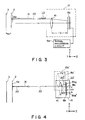
- Figures 2 and 3 are schematic representations, respectively, showing optical arrangements of a measuring system and a correcting system of this embodiment.
- Figure 4 is a schematic representation, for explaining a result of shift of the position of a pickup of the correcting system shown in Figure 3.
- Figure 5 is a schematic representation, for explaining a result of inclination of a mask in the correcting system shown in Figure 3.
- Figures 6A - 6D are schematic representations, respectively, showing optical paths in different portions.
- Figure 7 illustrates a known example of interval measuring device.
- Figure 1 is a perspective view, schematically showing a major portion of an embodiment of the present invention.
- Figures 2 and 3 illustrate optical principles of a measuring system and a correcting system of of the measuring device of this embodiment.
- the measuring system is a system for mainly measuring the interval between first and second objects.
- the correcting system is a system for mainly correcting a measurement error where a change occurs in the relative position or relative attitude of an illumination system and a light receiving system or in the relative attitude of a wafer (second object), relative to a mask (first object).
- a and 1b are beams of light from a light source LD such as, for example, a He-Ne laser, a semiconductor laser or LED.
- the light 1a is used in the measuring system, and the light 1b is used in the correcting system.
- a semiconductor laser is used as the light source LD.
- Denoted at 2 is a first object which is, in this example, a mask held fixed.
- Denoted at 3 is a second object which is a wafer, in this example.
- the mask 2 and the wafer 3 are disposed opposed to each other with an interval d0.
- Denoted at 4a and 5a are physical optic elements of the measuring system, provided for light reception and light emission, respectively, wherein these physical optic elements are formed in a portion of the mask 2 surface and are arrayed along the X-axis direction.
- Each of the physical optic elements 4a and 5a is provided by a diffraction grating or a zone plate, for example.
- the former has a size of about 30x30 (micron), and the latter has a size of about 30x60 (micron).
- denoted at 4b and 5b are physical optic elements of the correcting system, each comprising a diffraction grating.
- the former has a size of about 30x90 (micron), and the latter has a size of about 60x90 (micron).
- the light emission side physical optic element 5a of the measuring system has a pattern adapted to provide an angle of deflection for the emanating light which angle changes in dependence upon the position of incidence of the light thereupon.
- the optical element 5a has a refracting power effective to converge a received parallel light at a position 1000 microns above it.
- Denoted at 41 is a condensing lens system used in common for the measuring system and the correcting system.
- the lens system 41 has a focal length of f a .
- f a is about 30 mm.
- Denoted at 8a is a photodetector of the measuring system, and denoted at 8b and 8c are photodetectors of the correcting system.
- Each photodetector is disposed at the focal point position of the condenser lens 41, and each photodetector may comprise a line sensor having a function for detecting the position of incidence of a received light on its light receiving surface.
- Each of the photodetectors 8a, 8b and 8c has its elements arrayed in a direction parallel to the X-axis direction.
- Signal processing circuit 9a serves to process the signals from the photodetectors 8a, 8b and 8c, to determine the positions of light beams incident on the surfaces of the photodetectors 8a - 8c, respectively.
- a position sensitive detector may be used in place of the line sensor.
- an optical pickup head which comprises the condensing lens system 41 and the light receiving means 8a - 8c.
- the pickup head may include the signal processing circuit 9a and the light source LD.
- the pickup head is movable relative to the mask 2 or the wafer 3, and it is made movable at least along the mask 2.
- the diffraction grating 4a comprises straight grating elements having regular intervals. Diffracted light of a predetermined order or orders from the diffraction grating 4a, whose chief ray has been diffracted at an angle ⁇ 1 is obliquely inputted to a point B on the wafer 3 surface (a point C when the wafer 3 is at the position P2), and the inputted light is reflected thereby.
- Reflected light 31 is the reflected light when the wafer 3 is at the position P1 close to the mask, while reflected light 32 is the reflected light when the wafer 3 is at the position P2 which is displaced from the position P1 by a distance d G .
- Broken lines in Figure 2 depict the wafer 3 as it is at the position P2 and the optical path defined at that time.
- the reflected light 31 (32) from the wafer 3 is incident on a point D (E) which is on the surface of an off-axis type Fresnel zone plate (hereinafter "FZP") 5a of the first object 2.
- the FZP 5a has such an optical function that the angle of emission of the emerging diffraction light, diffracted thereby, changes in accordance with the position of incidence of the light inputted thereto.
- Diffraction light 61 (62) of a predetermined order or orders from the FZP 5a, diffracted at an angle ⁇ 2, is directed through the condensing lens system 41 to the surface of the light receiving means 8a.
- the interval between the mask 2 and the wafer 3 can be determined through calculation, which will be described later.
- each of the first and second physical optic elements (diffraction grating 4a and FZP 5a) provided on the mask 2 has a preset and known pitch and, therefore, the diffraction angle ⁇ 1 or ⁇ 2 of the diffraction light of a predetermined order or orders (e.g. positive and negative first orders), of the light inputted thereto, can be determined beforehand.
- a predetermined order or orders e.g. positive and negative first orders
- the quantity ⁇ S of displacement of the incident light upon the photodetector 8a surface with a unit change in the gap between the mask 2 and the wafer 3, namely, the sensitivity ⁇ S, is given by:
- the light 1b ( Figures 1 and 3) is projected to the physical optic element 4b of the mask by which the light is reflectively diffracted, such that reflectively diffracted light 22 emanates from the mask toward the photodetector 8b.
- the diffracted light 22 has a constant angle of emission independently of any change in the interval between the mask 2 and the wafer 3, and this light 22 is used as a reference light.
- the position of the gravity center of the light 22 incident on the photodetector 8b is used as a reference. Namely, the spacing between this reference position and the gravity center position of the light 61 (62) on the photodetector 8a surface with respect to the X-axis direction, is measured.
- the spacing between the gravity center positions of the light 22 and the light 61 with respect to the X-axis direction, as established when the wafer 3 is at a position (e.g. position P1) corresponding to the correct interval d R (d R d0) to be defined between the mask 2 and the wafer 3, is used as a reference spacing.
- the actually measured spacing mentioned above is compared with this reference spacing to determine the difference therebetween.
- the change d G in the mask-to-wafer gap, from the correct gap position P1 of the wafer is detected to determine the interval between the mask and the wafer.
- the spacing between the gravity center positions of the two lights with respect to the X-axis direction as the correct gap d R is given, can be detected beforehand by using design values of the mark and the device, for example.
- the light incident on the photodetector 8a surface displaces by 18 microns.
- a position sensitive detector having a position resolution of 0.3 micron is used as the photodetector 8a, in principle, it is possible to measure the interval between the mask 2 and the wafer 3 with a resolution of 0.02 micron or less.
- FZP physical optic element
- each of the physical optic elements 4b and 5b of the correcting system is provided by a diffraction grating comprising straight grating elements of regular intervals.
- the light 1b emanating from the semiconductor laser LD is obliquely inputted to the grating 4b of the mask 2, in the Z-Y plane, at a predetermined angle with respect to a normal to the mask 2 surface.
- positive first order reflectively diffracted light 22 passes through the condensing lens system 41 and enters the photodetector 8b accommodated in the optical pickup head (not shown).
- the diffraction grating 4b has a pattern of straight grating whose grating lines extend in an oblique direction, intersecting with the X axis at an angle ⁇ , in an orthogonal coordinate system where the longitudinal direction of the interval measuring rectangular mark region lies on the X axis while the widthwise direction thereof lies on the Y axis.
- the physical optic element (diffraction grating) 5b comprises a straight grating similar to the diffraction grating 4b, and it has a pattern of grating lines which extend, in an orthogonal X′-Y′ coordinate system on the wafer 3 surface having X′ and Y′ axes parallel to the axes of the aforementioned X-Y coordinate system, in an oblique direction intersecting with the X′ axis, for example, at an angle of ⁇ ′.
- Figures 6A and 6B show optical paths 22 and 25 of the correcting system, in the X-Z section and the Y-Z section, respectively.
- each of the photodetectors 8b and 8c for receiving the reference light 22 and 25, respectively is parallel to the X axis and it coincides with that of the photodetector 8a which receives the measuring light 61 (62).
- the light 1b impinges on the light entrance side physical optic element (diffraction grating) 4b of the mask 2.
- the diffraction grating 4b has such optical characteristic that, independently of the position of incidence, it emanates a received parallel light at a constant deflection angle depending on the angle of incidence of the light.
- Figures 4 and 5 illustrate the principle of the correcting system shown in Figure 3.
- the light 1b from the semiconductor laser LD is perpendicularly inputted to the grating 4b of the mask 2.
- the light 1b as well as the light 1a are portions of a single bundle of light supplied by the semiconductor laser LD.
- beams of light from separate light sources may be used.
- the light 1b may have the same wavelength as or a different wavelength from the light 1a used for the interval measurement.
- first order diffraction light having been reflectively diffracted by the diffraction grating 4b is directed through the condensing lens 41 to the surface of the photodetector 8b.
- FIG 4 broken lines depict the states of the light (22′) and the components of the optical pickup head 10 as the head 10 has shifted from its solid-line position, in the X-axis direction without any change in its attitude, and each component is denoted by the same reference numeral with dash.
- Reference numeral 8b2 ⁇ denotes the position of the point 8b2 when the optical pickup head 10 is at its solid-line position.
- the amount of displacement of the light 22 resulting from such translational shift is denoted by x a .
- the spacing between the light 61 (62) on the photodetector 8a and the light 22 on the photodetector 8b with respect to the X-axis direction does not change.
- broken lines 2′ and 24 depict the mask and the reference light as the mask 2 tilts by an angle ⁇ from its initial state, depicted by a solid line, because of the mask replacement or the like.
- ⁇ the angle from its initial state
- x b The quantity of displacement of the light due to such inclination of the mask.
- the angle ⁇ is within a sufficiently small range and that the length of the light path from the mask 2′ to the condensing lens 41 is substantially equal to the path length of the light 24, the light 61 impinging on the photodetector 8a displaces similarly by x b .
- the spacing between the light 61 (62) on the photodetector 8a and the light 22 on the photodetector 8b with respect to the X-axis direction does not change.
- the mask displaces in the X-axis direction or if the optical pickup head tilts, similarly, the spacing between two lights in the X-axis direction is unchangeable.
- adjustment may be made beforehand to ensure that the center of a photodetector for receiving the measuring light coincides with the center of a photodetector for receiving the reference light with respect to a predetermined direction.
- the position of incidence of the reference light upon the corresponding photodetector may be used as a reference point, and the spacing with respect to the predetermined direction between the reference point and the position of incidence of the measuring light upon the corresponding photodetector as measured in respect to the same detecting direction (e.g. X-direction) as the reference light, may be detected. Then, it is possible to measure the interval without being affected by any relative change between the head and the mask surface.
- a wafer chuck (not shown) for holding the wafer is moved upwardly or downwardly so that a correct interval is defined between the mask and the wafer.
- the reference light 25 is used to correct or compensate an error in the interval measurement caused by any relative inclination of the wafer 3 surface, relative to the mask 2 surface.
- the light transmissively diffracted at the first order, within the Y-Z plane, by the diffraction grating (physical optic element) 4b of the mask is perpendicularly incident on the wafer 3 surface and, by the diffraction grating (physical optic element) 5b, it is reflectively diffracted at the negative first order by the diffraction grating 5b within the Y-Z plane, whereby the reference light 25 is provided.
- the light 25 is transmitted through the mask 2 at the zero-th order and impinges on the photodetector 8c in the optical pickup head 10.
- the circuit 9a operates to detect the position of incidence of the light on the photodetector 8c, with respect to the same direction (X-axis direction) as the measuring light 61 (62).
- the reference light 25 is perpendicularly incident on the wafer surface.
- the photodetector 8c has a resolution ⁇ S for detection of the gravity center position of the light intensity and the measurement range for variation of the interval between the mask and the wafer (with respect to a reference set value) is denoted by ⁇ P
- the light is incident on the wafer surface substantially perpendicularly.
- the position of incidence of the reference light 25 upon the photodetector 8c can be regarded as substantially constant even if the interval between the mask and the wafer changes. Accordingly, it is possible to detect and correct any inclination of the wafer relative to the mask.
- the correction may be made by tilting the wafer chuck (not shown) for holding the wafer. After this correction, the interval detection and the interval adjustment described hereinbefore are executed.
- the light source LD is accommodated in the optical pickup head 10.
- the mask 2 surface is taken as a reference surface, there is a possibility that, due to displacement of the head 10 during plural printing and exposure processes, the angle of projection of the light 1a (1b) from the light source SL to the mask 2 surface (the angle as defined between the chief ray vector and a normal to the mask 2 surface) changes. This case will be explained below.
- the spacing between the first reference light 22 and the second reference light 25 on the sensor with respect to the X-axis direction does not correspond to the reference interval, i.e., the interval between the mask and the wafer as they are held parallel to each other.
- the reference interval i.e., the interval between the mask and the wafer as they are held parallel to each other.
- Figure 6D corresponds to a side view of that shown in Figure 6C.
- the spacing between the gravity center positions of the first and second reference lights 22 and 25 on the photodetectors 8b and 8c, with respect to the X-axis direction does not correspond to the reference spacing.
- the sequence of measurement may be such that, for example, a wafer stage is moved to move the wafer chuck so that the distance between the gravity center positions of the first and second reference lights 22 and 25 on the photodetectors 8b and 8c with respect to the X-axis direction becomes equal to a reference value and, then, the inclination of the wafer 3 surface is adjusted so that it becomes parallel to the mask 2 surface.
- the above-described reference value may be determined beforehand by light ray tracing simulation during design of each mark, for example.
- the interval between the mask and the wafer may be controlled so that the spacing between the gravity center positions of the first reference light 22 and the signal light 61 upon the photodetectors 8b and 8a becomes equal to the reference spacing as predetermined.
- the spacing between the gravity center positions of the first and second reference lights upon the photodetectors 8b and 8c with respect to the X-axis direction is held at the reference value having been set beforehand.
- an array of three photodetectors are used to receive three reflected beams from the mask and the wafer, independently of each other.
- a single photodetector such as an image pickup device having light receiving elements arrayed two-dimensionally, may be used to receive the three reflected beams to detect their incident positions, respectively.
- the three reflected beams are directed to the photodetecting means by using a single condensing lens system
- three separate condensing lens systems may be used to direct the three reflected beams to the photoelectric converting means, separately from each other.
- each of the diffraction patterns of the mask and the wafer for the reference light comprises a diffraction pattern having no optical power
- the structure of the diffraction pattern is not limited thereto.
- the wafer may be patterned so that no diffraction pattern is formed at the location at which the measuring light impinges.
- the device of the present invention is particularly suitably usable in a proximity type exposure apparatus.
- the invention is not limited to the application to this type of exposure apparatus.
Landscapes
- Physics & Mathematics (AREA)
- General Physics & Mathematics (AREA)
- Length Measuring Devices By Optical Means (AREA)
- Exposure And Positioning Against Photoresist Photosensitive Materials (AREA)
- Automatic Focus Adjustment (AREA)
- Exposure Of Semiconductors, Excluding Electron Or Ion Beam Exposure (AREA)
Applications Claiming Priority (2)
| Application Number | Priority Date | Filing Date | Title |
|---|---|---|---|
| JP2013263A JP2756331B2 (ja) | 1990-01-23 | 1990-01-23 | 間隔測定装置 |
| JP13263/90 | 1990-01-23 |
Publications (3)
| Publication Number | Publication Date |
|---|---|
| EP0439322A2 true EP0439322A2 (de) | 1991-07-31 |
| EP0439322A3 EP0439322A3 (en) | 1992-04-01 |
| EP0439322B1 EP0439322B1 (de) | 1996-11-27 |
Family
ID=11828332
Family Applications (1)
| Application Number | Title | Priority Date | Filing Date |
|---|---|---|---|
| EP91300463A Expired - Lifetime EP0439322B1 (de) | 1990-01-23 | 1991-01-22 | Verfahren und Vorrichtung zur Messung des Spaltes zwischen zwei einander gegenüberliegenden Objekten |
Country Status (4)
| Country | Link |
|---|---|
| US (1) | US5196711A (de) |
| EP (1) | EP0439322B1 (de) |
| JP (1) | JP2756331B2 (de) |
| DE (1) | DE69123267D1 (de) |
Families Citing this family (13)
| Publication number | Priority date | Publication date | Assignee | Title |
|---|---|---|---|---|
| JP3008654B2 (ja) * | 1992-02-21 | 2000-02-14 | キヤノン株式会社 | 位置検出装置 |
| US5519492A (en) * | 1992-06-27 | 1996-05-21 | Dr. Johannes Heidenhain Gmbh | Optical arrangement for detecting the intensity modulation of partial ray beams |
| DE69324532T2 (de) * | 1992-07-15 | 1999-09-23 | Nikon Corp., Tokio/Tokyo | Lichtquelle für ein Heterodyninterferometer |
| US5585923A (en) * | 1992-11-14 | 1996-12-17 | Canon Kabushiki Kaisha | Method and apparatus for measuring positional deviation while correcting an error on the basis of the error detection by an error detecting means |
| JP3428705B2 (ja) * | 1993-10-20 | 2003-07-22 | キヤノン株式会社 | 位置検出装置及びそれを用いた半導体素子の製造方法 |
| US5625453A (en) * | 1993-10-26 | 1997-04-29 | Canon Kabushiki Kaisha | System and method for detecting the relative positional deviation between diffraction gratings and for measuring the width of a line constituting a diffraction grating |
| US5550635A (en) * | 1993-10-29 | 1996-08-27 | Canon Kabushiki Kaisha | Rotational deviation detecting method and system using a periodic pattern |
| JP3368017B2 (ja) * | 1993-10-29 | 2003-01-20 | キヤノン株式会社 | 位置検出装置及びそれを用いた半導体素子の製造方法 |
| JP3158878B2 (ja) * | 1994-07-28 | 2001-04-23 | 松下電器産業株式会社 | 光学式エンコーダ |
| JPH0886612A (ja) * | 1994-09-19 | 1996-04-02 | Canon Inc | 光ヘテロダイン干渉を利用した位置ずれ検出装置 |
| JPH1022213A (ja) * | 1996-06-28 | 1998-01-23 | Canon Inc | 位置検出装置及びそれを用いたデバイスの製造方法 |
| JPH11241908A (ja) | 1997-12-03 | 1999-09-07 | Canon Inc | 位置検出装置及びそれを用いたデバイスの製造方法 |
| CN116819884B (zh) * | 2023-08-31 | 2023-11-14 | 光科芯图(北京)科技有限公司 | 掩模倾斜角度测量装置及曝光设备 |
Family Cites Families (17)
| Publication number | Priority date | Publication date | Assignee | Title |
|---|---|---|---|---|
| FR2436967A1 (fr) * | 1978-09-19 | 1980-04-18 | Thomson Csf | Procede d'alignement optique de motifs dans deux plans rapproches et dispositif d'alignement mettant en oeuvre un tel procede |
| US4596467A (en) * | 1984-03-16 | 1986-06-24 | Hughes Aircraft Company | Dissimilar superimposed grating precision alignment and gap measurement systems |
| JPS61111402A (ja) * | 1984-11-06 | 1986-05-29 | Nippon Kogaku Kk <Nikon> | 位置検出装置 |
| EP0243520B1 (de) * | 1986-04-29 | 1991-11-27 | Ibm Deutschland Gmbh | Interferometrische Maskensubstratausrichtung |
| US4815854A (en) * | 1987-01-19 | 1989-03-28 | Nec Corporation | Method of alignment between mask and semiconductor wafer |
| JPH01285803A (ja) * | 1988-05-13 | 1989-11-16 | Fujitsu Ltd | フレネル・ゾーン・プレートおよびそれを用いる位置合せ方法 |
| EP0309281B1 (de) * | 1987-09-25 | 1995-03-08 | Matsushita Electric Industrial Co., Ltd. | Vorrichtung zur Kontrolle des Lageverhältnisses zwischen einer Photomaske und einem Plättchen |
| DE68923018T2 (de) * | 1988-02-16 | 1995-11-09 | Canon K.K., Tokio/Tokyo | Verfahren und Vorrichtung zum Messen eines Zwischenraumes zwischen zwei Objekten. |
| JP2556126B2 (ja) | 1988-02-16 | 1996-11-20 | キヤノン株式会社 | 間隔測定装置及び間隔測定方法 |
| JP2546364B2 (ja) * | 1988-02-16 | 1996-10-23 | キヤノン株式会社 | 位置合わせ装置 |
| EP0329433A3 (de) * | 1988-02-16 | 1989-10-25 | Canon Kabushiki Kaisha | Verfahren und Vorrichtung zur Feststellung der Lage |
| DE68901933T2 (de) * | 1988-02-16 | 1992-12-24 | Canon Kk | Vorrichtung zur lagefeststellung. |
| DE68925142T2 (de) * | 1988-02-16 | 1996-06-13 | Canon K.K., Tokio/Tokyo | Vorrichtung zum Nachweis der örtlichen Beziehung zwischen zwei Objekten |
| JP2643270B2 (ja) | 1988-04-06 | 1997-08-20 | キヤノン株式会社 | 間隔測定装置 |
| JP2676933B2 (ja) * | 1988-09-05 | 1997-11-17 | キヤノン株式会社 | 位置検出装置 |
| JP2546350B2 (ja) | 1988-09-09 | 1996-10-23 | キヤノン株式会社 | 位置合わせ装置 |
| JP2734004B2 (ja) * | 1988-09-30 | 1998-03-30 | キヤノン株式会社 | 位置合わせ装置 |
-
1990
- 1990-01-23 JP JP2013263A patent/JP2756331B2/ja not_active Expired - Fee Related
-
1991
- 1991-01-22 EP EP91300463A patent/EP0439322B1/de not_active Expired - Lifetime
- 1991-01-22 US US07/643,475 patent/US5196711A/en not_active Expired - Fee Related
- 1991-01-22 DE DE69123267T patent/DE69123267D1/de not_active Expired - Lifetime
Also Published As
| Publication number | Publication date |
|---|---|
| DE69123267D1 (de) | 1997-01-09 |
| US5196711A (en) | 1993-03-23 |
| JP2756331B2 (ja) | 1998-05-25 |
| JPH03216505A (ja) | 1991-09-24 |
| EP0439322A3 (en) | 1992-04-01 |
| EP0439322B1 (de) | 1996-11-27 |
Similar Documents
| Publication | Publication Date | Title |
|---|---|---|
| EP0409573B1 (de) | Verfahren zum Feststellen von Lageabweichungen | |
| JP2704001B2 (ja) | 位置検出装置 | |
| US5200800A (en) | Position detecting method and apparatus | |
| EP0439322B1 (de) | Verfahren und Vorrichtung zur Messung des Spaltes zwischen zwei einander gegenüberliegenden Objekten | |
| US5235408A (en) | Position detecting method and apparatus | |
| EP0494789A2 (de) | Ausrichtverfahren | |
| US5343291A (en) | Method and apparatus for measuring an interval between two objects | |
| JP2676933B2 (ja) | 位置検出装置 | |
| US5325176A (en) | Position detecting method and apparatus including Fraunhofer diffraction detector | |
| EP0336537A1 (de) | Vorrichtung zum Nachweis der örtlichen Beziehung zwischen zwei Objekten | |
| US5294980A (en) | Positioning detecting method and apparatus | |
| JP2513300B2 (ja) | 位置検出装置 | |
| US5229617A (en) | Position detecting method having reflectively scattered light prevented from impinging on a detector | |
| JP2556126B2 (ja) | 間隔測定装置及び間隔測定方法 | |
| JP2827251B2 (ja) | 位置検出装置 | |
| JP2698446B2 (ja) | 間隔測定装置 | |
| JP2827250B2 (ja) | 位置検出装置 | |
| EP0358511A2 (de) | Vorrichtung zur Detektion der Positionsrelation zwischen zwei Objekten | |
| EP0332300B1 (de) | Verfahren und Vorrichtung zum Messen eines Zwischenraumes zwischen zwei Objekten | |
| JP2556559B2 (ja) | 間隔測定装置 | |
| EP0329433A2 (de) | Verfahren und Vorrichtung zur Feststellung der Lage | |
| JP2623757B2 (ja) | 位置合わせ装置 | |
| JP2862307B2 (ja) | 位置ずれ検出方法 | |
| JP2546317B2 (ja) | 位置合わせ装置 | |
| EP0410802A2 (de) | Verfahren zur Positionsdetektion |
Legal Events
| Date | Code | Title | Description |
|---|---|---|---|
| PUAI | Public reference made under article 153(3) epc to a published international application that has entered the european phase |
Free format text: ORIGINAL CODE: 0009012 |
|
| AK | Designated contracting states |
Kind code of ref document: A2 Designated state(s): DE FR GB NL |
|
| PUAL | Search report despatched |
Free format text: ORIGINAL CODE: 0009013 |
|
| AK | Designated contracting states |
Kind code of ref document: A3 Designated state(s): DE FR GB NL |
|
| 17P | Request for examination filed |
Effective date: 19920817 |
|
| 17Q | First examination report despatched |
Effective date: 19931105 |
|
| GRAH | Despatch of communication of intention to grant a patent |
Free format text: ORIGINAL CODE: EPIDOS IGRA |
|
| GRAH | Despatch of communication of intention to grant a patent |
Free format text: ORIGINAL CODE: EPIDOS IGRA |
|
| GRAH | Despatch of communication of intention to grant a patent |
Free format text: ORIGINAL CODE: EPIDOS IGRA |
|
| GRAA | (expected) grant |
Free format text: ORIGINAL CODE: 0009210 |
|
| AK | Designated contracting states |
Kind code of ref document: B1 Designated state(s): DE FR GB NL |
|
| PG25 | Lapsed in a contracting state [announced via postgrant information from national office to epo] |
Ref country code: NL Free format text: LAPSE BECAUSE OF FAILURE TO SUBMIT A TRANSLATION OF THE DESCRIPTION OR TO PAY THE FEE WITHIN THE PRESCRIBED TIME-LIMIT Effective date: 19961127 Ref country code: FR Effective date: 19961127 |
|
| REF | Corresponds to: |
Ref document number: 69123267 Country of ref document: DE Date of ref document: 19970109 |
|
| PG25 | Lapsed in a contracting state [announced via postgrant information from national office to epo] |
Ref country code: DE Effective date: 19970228 |
|
| EN | Fr: translation not filed | ||
| NLV1 | Nl: lapsed or annulled due to failure to fulfill the requirements of art. 29p and 29m of the patents act | ||
| PLBE | No opposition filed within time limit |
Free format text: ORIGINAL CODE: 0009261 |
|
| STAA | Information on the status of an ep patent application or granted ep patent |
Free format text: STATUS: NO OPPOSITION FILED WITHIN TIME LIMIT |
|
| 26N | No opposition filed | ||
| REG | Reference to a national code |
Ref country code: GB Ref legal event code: IF02 |
|
| PGFP | Annual fee paid to national office [announced via postgrant information from national office to epo] |
Ref country code: GB Payment date: 20040108 Year of fee payment: 14 |
|
| PG25 | Lapsed in a contracting state [announced via postgrant information from national office to epo] |
Ref country code: GB Free format text: LAPSE BECAUSE OF NON-PAYMENT OF DUE FEES Effective date: 20050122 |
|
| GBPC | Gb: european patent ceased through non-payment of renewal fee |
Effective date: 20050122 |