EP0438193A2 - Appareil d'affichage et méthode pour la mise en oeuvre d'un tel appareil - Google Patents
Appareil d'affichage et méthode pour la mise en oeuvre d'un tel appareil Download PDFInfo
- Publication number
- EP0438193A2 EP0438193A2 EP19910200041 EP91200041A EP0438193A2 EP 0438193 A2 EP0438193 A2 EP 0438193A2 EP 19910200041 EP19910200041 EP 19910200041 EP 91200041 A EP91200041 A EP 91200041A EP 0438193 A2 EP0438193 A2 EP 0438193A2
- Authority
- EP
- European Patent Office
- Prior art keywords
- array
- values
- texture
- texel
- texture memory
- Prior art date
- Legal status (The legal status is an assumption and is not a legal conclusion. Google has not performed a legal analysis and makes no representation as to the accuracy of the status listed.)
- Granted
Links
Images


Classifications
-
- G—PHYSICS
- G06—COMPUTING; CALCULATING OR COUNTING
- G06T—IMAGE DATA PROCESSING OR GENERATION, IN GENERAL
- G06T15/00—3D [Three Dimensional] image rendering
- G06T15/50—Lighting effects
-
- G—PHYSICS
- G06—COMPUTING; CALCULATING OR COUNTING
- G06F—ELECTRIC DIGITAL DATA PROCESSING
- G06F3/00—Input arrangements for transferring data to be processed into a form capable of being handled by the computer; Output arrangements for transferring data from processing unit to output unit, e.g. interface arrangements
- G06F3/14—Digital output to display device ; Cooperation and interconnection of the display device with other functional units
Definitions
- the invention relates to a display apparatus including a display processor having associated texture memory for storing a pyramidal or part-pyramidal array of texture element ("texel") values comprising a plurality of two-dimensional (2-D) arrays represesenting a 2-D modulation pattern at at least two distinct levels of resolution, the display processor further comprising for receiving a primitive description, which description includes an indication that the stored modulation pattern is to be mapped onto a primitive for display, means for generating 2-D coordinate pairs addressing texel values in a stored 2-D array to effect the mapping of the stored modulation pattern onto the primitive, and 2-D interpolating means responsive to fractional parts of the said 2-D coordinate pairs for combining together a number of texel values from the addressed array so as to generate an interpolated texel value.
- texel texture element
- the invention further relates to a method of operating such a display apparatus.
- An apparatus of the type set forth in the opening paragraph is described in WO 85/00913 and provides real-time synthesis and display of images representing three-dimensional scenes for flight simulation.
- the apparatus implements a technique known in the art as "texture mapping", in which a 2-D pattern (the “texture”) is pre-generated and stored in the texture memory, whereupon a single primitive is then rendered (transformed from "object space” into “screen space” and scanned into the display memory) with the texture mapped onto it.
- the technique enables a large amount of surface detail to be represented without a corresponding increase in the number of primitives that have to be rendered to produce an image.
- the stored pattern defines the colour of an object's surface, so that the texel values may constitute the colour values which may be written directly into the display memory.
- the texel values may be subjected to or otherwise control further processing, for example to allow the rapid calculation of complex lighting effects.
- Texture mapping can be implemented entirely in software, but in the context of the present invention we are concerned with hardware implementations in the field of real-time image synthesis. To avoid aliasing effects, it is necessary to filter the texel values during mapping. To simplify the computation of filtered values the known apparatus stores textures in so-called pyramidal arrays, comprising a succession of 2-D arrays, each pre-filtered to a different level of resolution. A simple 2-D interpolating means such as a bilinear interpolator is then sufficient, since each interpolated value is generated from a small and constant patch of texel values in the appropriate 2-D array. The generation and storage of pyramidal texture arrays are described by Lance Williams in a paper entitled "Pyramidal Parametrics" in Computer Graphics, Volume 17, No. 3 (Proc. SIGGRAPH 1983) at pages 1 to 11.
- the generation of a pre-filtered pyramidal array is conventionally undertaken by software running on the host processor.
- the successive 2-D arrays of the pyramid in the host memory are generated from a large highest-level array received from a source, for example a video camera, to obtain the texture of a natural object, or may be generated by calculations of lighting etc. using data defining the 3-D object space being depicted.
- This software process of pre-filtering can be very slow because a large number of memory accesses are involved in generating each filtered value from a patch of higher-resolution texel values.
- each texel value may comprise several independent components (R, G, B, for example) which must be interpolated separately in the conventional host processor.
- texture pyramids cannot be generated only when required for real-time display: all levels of all texture pyramids that may be required must be generated before commencing real-time image synthesis. This can lead to a very large part of main memory space being occupied by texture arrays that are never used. It also rules out the use of textures that may vary depending on how the 3-D model develops. For example it is known for texture maps to be used to define reflection patterns in a technique known as "environment mapping". If an object moves into the environment in the course of a simulation, the environment map should ideally change accordingly.
- the invention provides a display apparatus as set forth in the opening paragraph characterized in that the apparatus further comprises feedback means whereby interpolated texel values generated by the 2-D interpolating means from one 2-D array can be stored back in the texture memory to form a further 2-D array of the pyramidal or part-pyramidal array.
- the invention also provides a method of operating a display apparatus constructed in accordance with the invention as set forth in the preceding paragraph, the method comprising the steps of:
- the invention makes use of the recognition that, if the means within the display processor are caused to scan the stored 2-D array systematically but at a low density by generating appropriately spaced 2-D coordinate pairs, then the series of values generated by the interpolator, which would conventionally be used to define pixel values in the display memory, can be made to have the same values that are required to form a 2-D array representing the same pattern at a lower-resolution.
- the steps (b) and (c) of the method can be repeated or not to generate as many or as few levels of the pyramid as are required.
- the invention saves memory space in the main memory, which need then only store the highest level of a given pyramid (and perhaps one other medium-level array in case only low resolution is called for). Also, the speed of generation of the pyramid will generally be much faster when performed by the display processor hardware than when performed by the host processor. For example, special addressing hardware will be provided in the display processor, and the interpolation means will often contain three parallel interpolators, one each for red, green and blue component values, whereas the host processor processes these components serially.
- the texture memory may comprise separate first and second parallel-addressable texture memory banks while the feedback means are arranged to store the further 2-D array in a different one of the said texture memory banks to that in which the one 2-D array is stored, thereby enabling the read-out of texel values from the one 2-D array for supply to the interpolation means to be performed in parallel with the storage of interpolated values to form the further 2-D array.
- the 2-D coordinate generating means and the feedback means are arranged to generate and store successively lower-resolution levels of the pyramidal array alternately in the first and second texture memory banks.
- the texture memory may be divided (or further divided) into at least three parallel-addressed memories while the 2-D array storage means are arranged to distribute the texel values of each 2-D array in an interleaved manner so that values for a 2-D patch of texels may be read in parallel from the texture memory (or from each of the first and second texture memory banks, where provided), the interpolation means being arranged to combine 2-D interpolation within each patch with inter-level interpolation to generate a single 3-D interpolated value from two patches comprising six or more stored texel values. This allows very rapid readout of texel values for display, requiring no more memory read cycles than would be required to perform simple point sampling.
- the interpolation means may include first and second 2-D interpolators, for performing 2-D interpolation between the values within 2-D patches stored in first and second texture memory banks respectively, while the feedback means provides means whereby texel values read from a 2-D array stored in one texture memory bank and interpolated by the first 2-D interpolator may be written into a further 2-D array in another texture memory bank.
- the texture memory may comprise a linearly-addressed memory, the display processor further comprising physical address generating means for receiving a 2-D coordinate pair and for generating therefrom a linear physical address for application to the texture memory.
- the use of a linear texture address space allows more efficient use of the available texture memory.
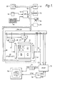
- FIG. 1 is a block diagram of a display apparatus including a known type of texture mapping hardware.
- a keyboard 10 and a tracker ball-type input device 12 provide input from a user to a central processing unit (CPU) 14.
- the tracker ball may be used for designing 3-D objects to be manipulated by the system, in a known manner.
- Other input devices may also be used, of course, such as a joystick, digitising tablet, or a "mouse". Such devices may also be used to manipulate images created by rotating, zooming etc. In general, such devices can be used more intuitively and efficiently than a conventional keyboard alone.
- Objects and also photographic images to be applied to object surfaces by texture mapping can also be input from a video source such as a camera 16.
- the CPU 14 is connected via a bus 18 (for example a VME bus) to a disc store 20, a ROM 22 and a main memory (MRAM) 24.
- the disc store which may include magnetic floppy discs, hard discs, and/or optical memory discs, is used for storing data (for example images or 3-D model data) which can then be recalled and manipulated to generate new images as desired.
- data may include the user's work from previous input sessions, and/or commercially generated data, for example for use in interactive computer-aided design or computer simulations for education or entertainment.
- data will generally be stored as polygonal model data rather than in the form of two-dimensional images.
- the data corresponds to a 3-D model containing objects which are typically broken down into groups of polygonal surfaces (primitives) in a 3-D "object" space (triangular or quadrilateral surfaces for example).
- the data for each object in the model comprises a list giving the position and nature of every polygon that goes to make up the object, including the relative positions of its vertices and the colour or transparency of the polygon surface.
- primitives may comprise curved surface patches, as is known in the art. It is known that a "texture" can be specified for mapping onto the surface, so that detail can be represented without increasing the number of primitives that make up the scene.
- a texture map is a stored 2-D array of texture element ("texel") values defining a 2-D pattern of modulation that may for example define the colour of pixels in a manner to described below.
- the texture may alternatively modulate other quantities such as reflectance or surface normal direction, as is known in the art.
- These texture maps may also be stored in the disc store 20 and recalled as required.
- the CPU 14 and the other components of the system then translate the 3-D model "world” in object space into a two-dimensional view for the user (in “viewer” space), from whatever viewpoint the user chooses, by means of geometric transformations effecting translations, rotations and perspective projections, generally by means matrix multiplication of vertex coordinates.
- the CPU 14 may also perform clipping and lighting calculations on a per-primitive or per-vertex basis.
- the ROM 22 and MRAM 24 provide program memory and workspace for the CPU 14, which may comprise a microprocessor, such as a Motorola MC68020.
- Special processing hardware 26 may be provided to assist the CPU 14 to perform the large number of arithmetic operations required to convert all but the simplest models into a two-dimensional scene.
- the hardware 26 may comprise standard arithmetic circuits or it may include more powerful custom-built or programmable digital signal processing (DSP) integrated circuits, and may be connected to the CPU 14 for example via a VME bus connection.
- DSP digital signal processing
- a display processing unit (DPU) 28 is connected between outputs of the CPU 14 (the bus 18) and inputs of a display memory (VRAM) 30.
- the display memory 30 stores pixel data COL in raster-scan format.
- the pixel data COL might typically include for each pixel three 8-bit values (total 24 bits) corresponding to red (R) green (G) and blue (B) components of the desired image.
- R red
- G green
- B blue
- the primitives are "scan converted" so that they may be drawn into the display memory 30.
- Scan conversion is a process whereby the pixels covered by each primitive are written row by row and pixel by pixel, in the same way that the complete image will be scanned for output to the display.
- a timing unit (video controller) 32 generates read-address signals XD and YD to address the pixel data within the VRAM 30 synchronously with the raster-scanning of a display screen 34. In response to these address signals, the locations in the VRAM 30 are scanned row by row and column by column to read colour values COLD which are fed to a digital to analogue converter (DAC) 36. If a non-RGB colour code is used, a matrix circuit or colour look-up table may be provided to translate the pixel data COLD into the equivalent RGB signal for supply to the display screen 34, which may for example be a cathode-ray tube (CRT) display screen.
- the display 34 directly or indirectly, also receives timing signals (SYNC) from the timing unit 32.
- the CPU 14 causes registers within the DPU 28 to be loaded, via the bus 18, with values defining a single primitive (for example in terms of vertex coordinates, edge slope and so on) and its various attributes - colour, reflectance and so forth.
- the DPU 28 then generates pixel coordinates (X and Y) so as to scan systematically the entire area covered by the primitive.
- the pixel coordinates X and Y are applied as write addresses to the VRAM 30, so that a pixel value COL can be written into the VRAM 30 for every pixel.
- the pixel values COL can be generated so that a basic surface colour of the primitive is modulated to account realistically for attributes of an object's surface (for example colour, transparency, diffuse reflectance, specular reflectance) and of the 3-D environment (for example locations, colours and shapes of light sources, distance haze).
- This modulation can be generated arithmetically from parameters loaded with the primitive data, for example to produce smoothly varying shading to simulate a curved surface.
- mapping hardware such as that referenced 40 to supply modulation values MOD according to a predetermined pattern stored in advance in a texture memory 41.
- the DPU 28 generates a pair of texture coordinates U and V simultaneously with each pair of pixel (display) coordinates X and Y so that the modulation pattern is mapped onto the primitive surface, implementing geometric transformations (i) from texture space into object space and (ii) from object space into viewer (display) space.
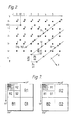
- Figure 2 provides an illustration of the relationship between texture space, defined by the horizontal and vertical axes labelled U and V, and screen space defined by the oblique axes X and Y.
- the actual stored texel values correspond to integer values of U and V and are represented by a square array of solid circular dots.
- the locations of the pixels in screen space are marked by diagonal crosses ('x') and lie along scanlines referenced S1, S2 and S3 etc. parallel to the X-axis.
- the CPU 14 may for example provide the DPU 28 in advance with the coordinate pair (U0,V0) corresponding to the first pixel on scanline S1, and also partial derivatives ⁇ U/ ⁇ X and ⁇ V/ ⁇ X defining the slope of the screen space scanlines S1 etc. in texture space and partial derivatives ⁇ U/ ⁇ Y and ⁇ V/ ⁇ Y defining the slope of the pixel columns in texture space.
- the transformation from texture space to screen space is linear.
- the scanlines S1 etc. and the pixel columns might diverge or converge, or even curve, in which case the partial derivatives vary from point to point across the primitive.
- the texture coordinates U and V are processed within the mapping hardware 40 in a manner to be described below and applied to the texture memory 41 so that a modulation value MOD is available for each pixel location X,Y being addressed.
- the value MOD commonly comprises a colour value, and in principle it could directly form the pixel value COL and be fed directly into the display memory (VRAM) 30, as shown by the dotted data path 42. More commonly, however, even if the values MOD are colour values, they will require to be modified within the DPU 28 to allow for realistic lighting effects. In a more general case, the modulation values MOD are used within the DPU 28 together with other parameters to modify the pixel values COL less directly.
- mapping For example, in so-called “bump mapping”, the values MOD modulate the surface normal direction of the primitive, so as to affect subsequent lighting calculations and so, indirectly, the pixel values COL.
- environment mapping uses the TRAM to store an image of the environment, for example using U and V as spherical coordinates, so that specular reflections of a complex environment (including light sources, windows, other objects and so on) can be simulated.
- the texels represented in the texture memory 41 will not in general correspond on a one-to-one basis with the pixels of the display and, in particular when the primitive is shown in the distance and the texture is consequently mapped onto a very small number of pixels, two-dimensional spatial filtering is required to avoid the aliasing effects that would be disturbing to the viewer if simple sub-sampling were used.
- the reference Williams describes the conventional solution to this which is to store several 2-D arrays (hereinafter referred to as "maps") for a given pattern, each being successively smaller and pre-filtered to a successively lower resolution.
- the DPU 28 then need only produce a level coordinate L to determine the appropriate map to use.
- the maps may be chosen to be square, having power-of-two dimensions, and be stored in a square texture memory according to the "multum in parvo" (“MIP map”) technique described by Williams.
- Figure 1 shows within the texture memory 41 the colour components R, G and B of a texture pyramid stored as a MIP map.
- each texel value comprises an 8-bit value for each of the R, G and B colour components
- the entire texture memory 41 is thus 1 Mbyte in size.
- the texel values are stored in the memory 41 in advance of rendering by the CPU 14 via the bus 18 and a writing port 43 of the memory 41.
- the DPU 28 For each texel value to be read, the DPU 28 generates a 2-D coordinate pair, each coordinate (U and V) of which includes at least an integer part 9 bits in length.
- the level coordinate L is generated by the DPU 28 and used to generate physical coordinates U′ and V′ from the "virtual" coordinates U and V for application to read address ports 44 and 45 respectively of the texture memory 41.
- the memory 41 releases the R, G and B components of an addressed texel via a (24-bit) read port 46.
- the required physical coordinates U′ and V′ can be generated simply by a pair of binary shifting circuits 47 and 48 respectively, each right-shifting the respective coordinate a number of places defined by the level coordinate L.
- the address corresponding to a given texel in the level 0 map can be converted to the physical address of the corresponding texel in the level L map can be found by right-shifting the U and V coordinates L places, effectively scaling-down each coordinate by 2 L .
- the level coordinate L can be supplied to the DPU 28 as part of the primitive data, but if perspective is to be accounted for in the mapping, then the level coordinate L will more probably be generated within the DPU on a per-pixel basis, dependent on the partial derivatives of U, V with respect to X, Y.
- the coordinates L, U′ and V′ can have fractional parts (Lf, Uf′ and Vf′) as well as integer parts (Li, Ui′, Vi′).
- the fractional parts of the U′ and V′ coordinates can be used to perform 2-D (for example, bilinear) interpolation between a square patch of four adjacent texels within one level, and the fractional part Lf of the level coordinate can be used to interpolate between (2-D interpolated) texel values from two adjacent levels of the pyramidal array.
- texture pyramids in the texture memory 41.
- three texture pyramids might define the shapes 'o', '+' and 'x' mapped onto the faces of the cube shown on the screen of the display 34 in Figure 1.
- the coordinate pairs U, V generated by the DPU 28 would then incorporate 2-D offsets to ensure that the correct part of the 2-D array is addressed.
- some of the space in the texture inevitably remains unused, effectively wasted. It is not possible in a general case to eliminate unused space from a mosaic of 2-D shapes.
- FIG. 3 shows novel mapping hardware that can be substituted for that shown at 40 in Figure 1.
- a linearly-addressed texture memory 41′ is provided, so that the problem of eliminating wasted space is readily solvable.
- a texture management circuit 49 keeps track of the various arrays within the linear memory 41′ and serves to convert the pyramidal coordinates L, U and V into linear physical texel addresses. Instead of using a 2-D offset to identify different textures all stored as a mosaic within a large map, the CPU 14 in the novel system supplies with the primitive data a texture identifying value T separate from the coordinates U and V. Any 2-D map forming part of a texture pyramid can thus be identified as map T.Li, where Li is the integer part of the level coordinate L.
- the circuit 49 is more complex than the simple 2-D MIP addressing hardware, but the improvement in memory utilisation and flexibility may be very great.
- the DPU 28′ in Figure 3 is a slightly modified version of the conventional DPU 28 ( Figure 1), having an output T for passing the received identifying value to the texture management circuit 49 .
- the modified DPU 28′ also has an output carrying a logic signal FB for activating feedback paths as described in a later part of this description.
- the novel hardware shown in Figure 3 also incorporates not only 2x2 patch addressing (to allow high-speed bilinear interpolation) but also a novel parallel structure so that eight texel values are available for trilinear interpolation simultaneously, yet without the excessive parallelism of the solution proposed by Williams.
- the texture memory 41′ is divided into two banks of memory, TRAM1 and TRAM2, and the system ensures that arrays T.Li and T.Li+1 for two adjacent levels of a given texture pyramid will always be stored in different banks TRAM1 and TRAM2.
- the texture management circuit 49 has inputs to receive the signals T, L, U and V from the DPU 28′.
- the texture management circuit includes a page location and logic circuit (PLLC) 50 which receives the texture identification T and at least the integer part Li of the level coordinate L supplied by the DPU.
- PLLC page location and logic circuit
- the PLLC 50 stores information defining for each map T.Li (i) in which bank TRAM1 or TRAM2 the map T.Li is stored, (ii) the width w(T.Li) of the map in the U-direction and (iii) a base address B(T.Li) locating the start of the linearly-stored array in the appropriate bank TRAM1 or TRAM2.
- the PLLC 50 supplies the stored data for the maps T.Li and T.Li+1 to the remainder of the circuit 49 which is thereby enabled to generate linear addresses A1 and A2 for application to the memory banks TRAM1 and TRAM2 respectively, so as to address the texel data for coordinate pair (U, V) in the levels Li and Li+1 in the texture pyramid T.
- su(T.Li) and sv(T.Li) represent generalised scale factors relating the dimensions of the map T.Li to those of the largest map (T.0) in the pyramid T, in the U ⁇ and V-directions respectively.
- the PLLC 50 in Figure 3 has outputs supplying values W1, B1, W2 and B2 defining the widths and base locations for the maps to be addressed in TRAM1 and TRAM2 respectively.
- an adder 51 is provided to generate the value Li+1 from the value Li generated by the DPU 28′.
- a multiplexer 52 responsive to the logic signal SWI1 selects either Li or Li+1 to generate the level coordinate L1 for the map stored in bank TRAM1.
- Another multiplexer 53 is responsive to the complementary logic signal SWI2 selects the other of Li and Li+1 to generate the level value L2 for the map stored in bank TRAM2.
- the scaled coordinates U1, V1, U2 and V2 are all separated into their integer parts U1i etc. and their fractional parts U1f etc.
- First and second left-shifters 58 and 59 receive the integer parts V1i and V2i of the scaled V coordinates V1 and V2 respectively and are responsive to the width indices W1 and W2 respectively so as to generate values 2 W1 .V1i and 2 W2 .V2i respectively, where 2 W1 and 2 W2 are the widths of the maps stored in the banks TRAM1 and TRAM2 respectively.
- An adder 60 adds the integer part of U1i of the first scaled U coordinate U1 to the value 2 W1 .V1i generated by the first left-shifter 58 to generate a first linear offset address I1.
- a further adder 61 adds the first offset address I1 to the first map base address B1 generated by the PLLC 50 to generate the first linear texel address A1 for application to the first bank TRAM1 of the texture memory 41′.
- a further adder 62 generates a second linear offset address I2 by adding the values U2i and 2 W2 .V2i
- a still further adder 63 adds the second linear offset address I2 to the record map base address B2 generated by the PLLC 50 to generate the second linear texel address A2 for application to the second bank TRAM2 of the texture memory 41′. Since the bits of value V1i (or V2i), once shifted, do not overlap with those of the value U1i (U2i), the adders 60 and 62 can in fact be implemented by simpler OR-gates.
- Each texture memory bank TRAM1 and TRAM2 is further divided as shown into four parts A, B, C, and D which can be addressed in parallel.
- the texel values defining a given map are distributed between the four parts A-D of the appropriate memory bank (TRAM1 or TRAM2) according to a predetermined pattern such as that illustrated by the letter A, B, C or D next to each texel value (solid circle) in Figure 2, so as to allow parallel addressing of a 2x2 patch of texels.
- a predetermined pattern such as that illustrated by the letter A, B, C or D next to each texel value (solid circle) in Figure 2, so as to allow parallel addressing of a 2x2 patch of texels.
- V even even
- texel values are stored alternately in parts A and B.
- odd-numbered lines V odd
- the values are stored alternately in parts C and D.
- a special address port 64 receives the linear texel address A1 from the output of adder 61 and generates therefrom four addresses A1A-A1D for application to the four memories TRAM1A to TRAM1D respectively, in response to which the texel values for the patch (U, V), (U+1, V), (U, V+1) and (U+1, V+1) become available via four corresponding read ports 65A-65D.
- the address port 64 receives the least significant bits U1ilsb and V1ilsb of the integer parts of the first scaled coordinate pair U1, V1, which define whether U1 and V1 respectively are odd or even.
- the patch addressing hardware 64, 65A-65D this can be similar to that used for transforming digitised video images, an example of which is shown in Figure 2 of an article "Transforming Digital Images in Real Time” by Joel H. Dedrick in ESD: The Electronic System Design Magazine, August 1987 at pages 81 to 85.
- One difference from the known hardware is necessitated by the linear storage of the texel arrays in the system shown in Figure 3.
- the Dedrick circuit which uses a 2-D addressable framestore memory
- a unit value 0001 is added to the vertical coordinate (Y′) to address the texel values in the next row (Y′+1) of the image.
- the address port 64 also receives the width index W1 generated by the PLLC 50 for the map stored in bank TRAM1.
- a similar patch address port 66 is provided for the second bank TRAM2 of the texture memory 41′ and receives the second linear address A2, odd/even indicators U2i1sb and V2i1sb and the second width index W2.
- the port 66 generates patch addresses A2A-A2D which are applied to respective parts A-D of the second texture memory bank TRAM2 which has four corresponding read ports 67A-67D.
- the four texel values from the read ports 65A-65D of bank TRAM1 are supplied to inputs of a first bilinear (2-D) interpolator BIL1 which also receives the fractional parts U1f and V1f of the first scaled coordinate pair U1,V1.
- the bilinear interpolator BIL1 combines the four texel values in the patch addressed by addresses A1A-A1D (derived from the integer parts U1i and V1i of the pair) so as to generate a first bilinearly interpolated texel value MOD1.
- the texel values from the read ports 67A-67D of bank TRAM2 are similarly applied to a second bilinear interpolator BIL2 which also receives the fractional parts U2f and V2f of the second scaled coordinate pair U2, V2 and generates a second bilinearly interpolated texel value MOD2.
- the two bilinearly interpolated values MOD1 and MOD2, one derived from the map T.Li and the other derived from the map T.Li+1 are then fed to a linear interpolator LINT.
- the interpolator LINT combines the values MOD1 and MOD2 in proportions determined by the fractional part Lf of the level coordinate L received from the DPU 28 to generate a trilinearly interpolated modulation value MOD for the pyramidal coordinates L, U and V.
- the value MOD may be used to effect a modulation of pixel colour values COL either directly (dotted path 42) or indirectly via further processing in the DPU 28′.
- each texel value will comprise three colour component values such as R, G and B, and the interpolators BIL1, BIL2 and LINT may in fact comprise three interpolators each, or may be adapted in some other way to perform the three-component interpolation.
- the hardware shown in Figure 3 also incorporates first and second feedback paths 70 and 72 so that the bilinearly interpolated values MOD1 from the first memory bank TRAM1 can be fed into a write port 71 of the second bank TRAM2 of the texture memory 41′ and the values MOD2 from the second bank TRAM2 can be fed into a write port 73 of the first bank TRAM1.
- the logic signal FB supplied by the DPU 28′ indicates in the '1' state that a feedback path is to be activated.
- AND gates 74 and 75 combine the signal FB with the logic signals SWI1 and SWI2 respectively generated by the PLLC 50 to generate a pair of logic signals FB1and FB2, respectively.
- each multiplexer 76 or 78 serves to connect the corresponding write ports 71 or 73 with the CPU 14 via the bus 18.
- Each memory bank constitutes a linear physical address space A1 or A2 respectively.
- the 2-D array (map) of texel values for level Li of map T is stored in linear form as a page of data referenced PT.Li. Texture 1 can be seen to have four pages P1.0, P1.1, P1.2 and P1.3, each one quarter of the linear size of the previous page. While P1.0 is stored in bank TRAM1, page P1.1 is stored in bank TRAM2, P1.2 in bank TRAM1 and so on, alternating for as many levels as are stored.
- a highest level page P2.0 exists, but, because it is not required at the time illustrated, it is not stored in the texture memory, so that more free space (shaded) is available to receive other maps as required.
- the memory map shown in Figure 4 may represent a time when many different maps, forming various levels of various texture pyramids, have been loaded, used and then deleted as the corresponding texture has become not required, or not required at such a high (or low) resolution.
- Figure 5 shows the contents of the page table memory PTAB, shown dotted within the page location and logic circuit PLLC 50 of Figure 3, which enables a given array T.Li to be found in the memory.
- a first item in each entry is a single bit value SWI1/ SWI2 which takes the value 1 or 0 depending on whether the page is stored in the bank TRAM1 or the bank TRAM2 respectively. This bit value therefore enables the logic circuit PLLC to generate the signals SWI1 and SWI2 to control the generation of the addresses A1 and A2 as described with reference to Figure 3.
- a second item in each entry in the table is the width index W of the map T.Li.
- a third item in each entry contains the base location B in the memory (TRAM1 or TRAM2) starting at which the texel values comprising that page are stored.
- the arrays of texel values forming the pages P1.0 etc. can be stored in the memory banks TRAM1 and TRAM2 by the CPU 14 via the bus 18 and write ports 71 and 73 respectively as shown. It is a straightforward matter of "housekeeping" for the CPU 14 to ensure that (i) any new page of texel data is stored in an otherwise unused part of the texture memories, (ii) each alternate level of a given pyramid is stored in a different bank TRAM1 or TRAM2 and (iii) that the page table PTAB in the PLLC 50 is at the same time loaded with the appropriate values of SWI1/ SWI2 , W and B. If enough space is not available in a single block for a new texture (perhaps P2.0 is to be loaded), then a "garbage collection" operation can be carried out to gather the unused areas together into a large enough area.
- Entire pyramidal texture arrays may be stored in a database in the disc store 20 or in the main memory 24, with the various 2-D level arrays (maps) being transferred to spare locations in the appropriate texture memory as required.
- the provision of the feedback paths 70 and 72 enables the bilinear interpolators BIL1 or BIL2 to be used as filters in a manner to be described below to generate maps for successive levels from a single, high resolution map loaded via the bus 18. This may be advantageous, since the hardware with patch-addressing and interpolation may provide a much faster filter than the conventional alternative which is a software routine executed by the CPU 14.
- Figure 6 shows a flowchart defining a sequence of operations performed to generate a filtered map T.Li+1 from a map T.Li previously stored in one bank of the texture memory 41′, using the feedback of values generated by the existing bilinear interpolators.
- the CPU 14 allocates texture memory space for the page PT.Li+1 by loading an entry comprising appropriate values SWI1/ SWI2 (T.Li+1), W(T.Li+1) and B(T.Li+1) in the page table PTAB within the PLLC 50.
- the DPU 28′ arranges that any values MOD generated by the linear interpolator LINT during the filtering process are ignored.
- step 88 the DPU 28′ is caused to "draw" the imaginary polygon, leading to the automatic generation of the desired filtered values MOD1 or MOD2 at the output of the bilinear interpolator BIL1 or BIL2, depending on whether the source map T.Li is stored in bank TRAM1 or TRAM2.
- the interpolated values are then automatically written into the locations in the other memory bank (TRAM2 or TRAM1) that were allocated for the map T.Li+1 in step 80.
- texture mapping hardware itself for map filtering and/or transfer has advantages over the conventional method using software running on the host computer, because the display processor hardware is already specialised for rapid addressing of texture arrays, including 2 x 12 patch addressing hardware, interpolating hardware geared to receive R, G and B in parallel, and so forth.
- This advantage can be readily appreciated by considering that filtering or transferring a 2-D array in this apparatus takes about the same amount of time as it would take to render a single, similarly sized polygon. This is an overhead that can generally be absorbed in real-time without a significant loss in performance since a typical system may already be rendering hundreds or even thousands of polygons in each image frame.
- map sizes and so forth imposed in the embodiment described simplify the construction, for example, of the PLLC 50 and allow the use of bit shifters 54 to 59 instead of complex multipliers. These limitations also simplify the allocation of space to new pages in the texture memory. Clearly, however, the design need not be limited to this case, and some variations will be enumerated below.
- the width index W would not need to be stored separately if it were known that a map's width was always 2 N-Li , where 2 N is the size of the largest permitted map.
- two level values Lu and Lv could be supplied, identifying a previously stored map of 2 N-Lui texels by 2 N-Lvi rows.
- Figure 7 illustrates one possible way of storing two pyramidal texture arrays (R1/G1/B1 and R2/G2/B2) in two two-dimensional texture memory banks 170 and 172.
- the allocation is similar to the conventional MIP map arrangement of Figure 2 but allows parallel read-out from adjacent levels of any one texture.
- the mapping hardware 40 of Figure 1 can be adapted to incorporate and take advantage of a dual texture memory in accordance with this scheme, to achieve parallel addressing of the two level maps required for inter-level interpolation.
- the provision of feedback paths analogous to the paths 70 and 72 ( Figure 3) would also allow the hardware to generate pyramids from single high-resolution maps.
Applications Claiming Priority (2)
| Application Number | Priority Date | Filing Date | Title |
|---|---|---|---|
| GB9000843 | 1990-01-15 | ||
| GB9000843A GB2240017A (en) | 1990-01-15 | 1990-01-15 | New, interpolated texture values are fed back to texture memories |
Publications (3)
| Publication Number | Publication Date |
|---|---|
| EP0438193A2 true EP0438193A2 (fr) | 1991-07-24 |
| EP0438193A3 EP0438193A3 (en) | 1991-11-13 |
| EP0438193B1 EP0438193B1 (fr) | 1998-09-09 |
Family
ID=10669302
Family Applications (1)
| Application Number | Title | Priority Date | Filing Date |
|---|---|---|---|
| EP91200041A Expired - Lifetime EP0438193B1 (fr) | 1990-01-15 | 1991-01-11 | Appareil d'affichage et méthode pour la mise en oeuvre d'un tel appareil |
Country Status (6)
| Country | Link |
|---|---|
| US (1) | US5544292A (fr) |
| EP (1) | EP0438193B1 (fr) |
| JP (1) | JP3007701B2 (fr) |
| KR (1) | KR100191112B1 (fr) |
| DE (1) | DE69130123T2 (fr) |
| GB (1) | GB2240017A (fr) |
Cited By (2)
| Publication number | Priority date | Publication date | Assignee | Title |
|---|---|---|---|---|
| EP0613098A2 (fr) * | 1993-02-25 | 1994-08-31 | Kabushiki Kaisha Toshiba | Appareil de traitement d'image et méthode pour commander celui-ci |
| WO2000030041A1 (fr) * | 1998-11-12 | 2000-05-25 | Sony Computer Entertainment Inc. | Procede et dispositif de generation d'image |
Families Citing this family (45)
| Publication number | Priority date | Publication date | Assignee | Title |
|---|---|---|---|---|
| GB9316214D0 (en) * | 1993-08-05 | 1993-09-22 | Philips Electronics Uk Ltd | Image processing |
| US5461712A (en) * | 1994-04-18 | 1995-10-24 | International Business Machines Corporation | Quadrant-based two-dimensional memory manager |
| GB9501832D0 (en) | 1995-01-31 | 1995-03-22 | Videologic Ltd | Texturing and shading of 3-d images |
| DE69635638T2 (de) * | 1995-06-06 | 2006-07-20 | Hewlett-Packard Development Co., L.P., Houston | Pufferspeicher für Texturdaten |
| US5745118A (en) * | 1995-06-06 | 1998-04-28 | Hewlett-Packard Company | 3D bypass for download of textures |
| US5872867A (en) * | 1995-08-04 | 1999-02-16 | Sarnoff Corporation | Method and apparatus for generating image textures |
| US6111584A (en) * | 1995-12-18 | 2000-08-29 | 3Dlabs Inc. Ltd. | Rendering system with mini-patch retrieval from local texture storage |
| GB2326806A (en) * | 1996-03-14 | 1998-12-30 | I I Interactive Innovations Lt | Computerized graphics systems |
| JPH11509653A (ja) * | 1996-05-17 | 1999-08-24 | フィリップス エレクトロニクス ネムローゼ フェンノートシャップ | 表示装置 |
| US5935198A (en) * | 1996-11-22 | 1999-08-10 | S3 Incorporated | Multiplier with selectable booth encoders for performing 3D graphics interpolations with two multiplies in a single pass through the multiplier |
| US6366290B1 (en) * | 1997-03-31 | 2002-04-02 | Cirrus Logic, Inc. | Dynamically selectable texture filter for a software graphics engine |
| US6130674A (en) * | 1997-03-31 | 2000-10-10 | Cirrus Logic, Inc. | Dynamically selectable texture filter for computer graphics |
| US20020154132A1 (en) | 1997-07-30 | 2002-10-24 | Alain M. Dumesny | Texture mapping 3d graphic objects |
| US6151029A (en) * | 1997-08-22 | 2000-11-21 | Seiko Epson Corporation | Texture mapping with improved technique for selecting an appropriate level in filtered representations of the texture |
| JP3630934B2 (ja) | 1997-08-29 | 2005-03-23 | 三洋電機株式会社 | テクスチャ記録方法 |
| US6188381B1 (en) * | 1997-09-08 | 2001-02-13 | Sarnoff Corporation | Modular parallel-pipelined vision system for real-time video processing |
| US6016151A (en) * | 1997-09-12 | 2000-01-18 | Neomagic Corp. | 3D triangle rendering by texture hardware and color software using simultaneous triangle-walking and interpolation for parallel operation |
| US6104413A (en) * | 1998-03-11 | 2000-08-15 | Industrial Technology Research Institute | Methods and systems for storing texels retrievable in a single cycle |
| US6175368B1 (en) * | 1998-03-24 | 2001-01-16 | Ati Technologies, Inc. | Method and apparatus for object rendering including bump mapping |
| US6191793B1 (en) | 1998-04-01 | 2001-02-20 | Real 3D, Inc. | Method and apparatus for texture level of detail dithering |
| US6204857B1 (en) | 1998-04-16 | 2001-03-20 | Real 3-D | Method and apparatus for effective level of detail selection |
| US6353438B1 (en) * | 1999-02-03 | 2002-03-05 | Artx | Cache organization—direct mapped cache |
| US6784882B1 (en) * | 1999-09-10 | 2004-08-31 | Sony Computer Entertainment Inc. | Methods and apparatus for rendering an image including portions seen through one or more objects of the image |
| US6717577B1 (en) | 1999-10-28 | 2004-04-06 | Nintendo Co., Ltd. | Vertex cache for 3D computer graphics |
| US6618048B1 (en) | 1999-10-28 | 2003-09-09 | Nintendo Co., Ltd. | 3D graphics rendering system for performing Z value clamping in near-Z range to maximize scene resolution of visually important Z components |
| US7196710B1 (en) | 2000-08-23 | 2007-03-27 | Nintendo Co., Ltd. | Method and apparatus for buffering graphics data in a graphics system |
| US6700586B1 (en) | 2000-08-23 | 2004-03-02 | Nintendo Co., Ltd. | Low cost graphics with stitching processing hardware support for skeletal animation |
| US7061502B1 (en) | 2000-08-23 | 2006-06-13 | Nintendo Co., Ltd. | Method and apparatus for providing logical combination of N alpha operations within a graphics system |
| US6937245B1 (en) | 2000-08-23 | 2005-08-30 | Nintendo Co., Ltd. | Graphics system with embedded frame buffer having reconfigurable pixel formats |
| US6811489B1 (en) | 2000-08-23 | 2004-11-02 | Nintendo Co., Ltd. | Controller interface for a graphics system |
| US6707458B1 (en) | 2000-08-23 | 2004-03-16 | Nintendo Co., Ltd. | Method and apparatus for texture tiling in a graphics system |
| US6636214B1 (en) | 2000-08-23 | 2003-10-21 | Nintendo Co., Ltd. | Method and apparatus for dynamically reconfiguring the order of hidden surface processing based on rendering mode |
| US7184059B1 (en) | 2000-08-23 | 2007-02-27 | Nintendo Co., Ltd. | Graphics system with copy out conversions between embedded frame buffer and main memory |
| US7538772B1 (en) | 2000-08-23 | 2009-05-26 | Nintendo Co., Ltd. | Graphics processing system with enhanced memory controller |
| US7576748B2 (en) | 2000-11-28 | 2009-08-18 | Nintendo Co. Ltd. | Graphics system with embedded frame butter having reconfigurable pixel formats |
| US6825851B1 (en) | 2000-08-23 | 2004-11-30 | Nintendo Co., Ltd. | Method and apparatus for environment-mapped bump-mapping in a graphics system |
| US7023447B2 (en) * | 2001-05-02 | 2006-04-04 | Eastman Kodak Company | Block sampling based method and apparatus for texture synthesis |
| US7190366B2 (en) * | 2004-05-14 | 2007-03-13 | Nvidia Corporation | Method and system for a general instruction raster stage that generates programmable pixel packets |
| US8411105B1 (en) | 2004-05-14 | 2013-04-02 | Nvidia Corporation | Method and system for computing pixel parameters |
| US7538773B1 (en) | 2004-05-14 | 2009-05-26 | Nvidia Corporation | Method and system for implementing parameter clamping to a valid range in a raster stage of a graphics pipeline |
| US8432394B1 (en) | 2004-05-14 | 2013-04-30 | Nvidia Corporation | Method and system for implementing clamped z value interpolation in a raster stage of a graphics pipeline |
| US8416242B1 (en) | 2004-05-14 | 2013-04-09 | Nvidia Corporation | Method and system for interpolating level-of-detail in graphics processors |
| US7079156B1 (en) * | 2004-05-14 | 2006-07-18 | Nvidia Corporation | Method and system for implementing multiple high precision and low precision interpolators for a graphics pipeline |
| US7595806B1 (en) | 2004-08-03 | 2009-09-29 | Nvidia Corporation | Method and system for implementing level of detail filtering in a cube mapping application |
| US8441497B1 (en) | 2007-08-07 | 2013-05-14 | Nvidia Corporation | Interpolation of vertex attributes in a graphics processor |
Citations (3)
| Publication number | Priority date | Publication date | Assignee | Title |
|---|---|---|---|---|
| GB2138252A (en) * | 1983-04-12 | 1984-10-17 | Marconi Co Ltd | Image generator |
| GB2171579A (en) * | 1985-02-20 | 1986-08-28 | Singer Link Miles Ltd | Apparatus for generating a visual display |
| EP0321291A2 (fr) * | 1987-12-18 | 1989-06-21 | General Electric Company | Microtexture pour détail rapproché |
Family Cites Families (3)
| Publication number | Priority date | Publication date | Assignee | Title |
|---|---|---|---|---|
| US4400768A (en) * | 1980-06-04 | 1983-08-23 | Burroughs Corporation | Parallel access computer memory system employing a power-of-two memory modules |
| US4615013A (en) * | 1983-08-02 | 1986-09-30 | The Singer Company | Method and apparatus for texture generation |
| US4797942A (en) * | 1987-03-02 | 1989-01-10 | General Electric | Pyramid processor for building large-area, high-resolution image by parts |
-
1990
- 1990-01-15 GB GB9000843A patent/GB2240017A/en not_active Withdrawn
-
1991
- 1991-01-11 EP EP91200041A patent/EP0438193B1/fr not_active Expired - Lifetime
- 1991-01-11 DE DE69130123T patent/DE69130123T2/de not_active Expired - Fee Related
- 1991-01-15 KR KR1019910000502A patent/KR100191112B1/ko not_active IP Right Cessation
- 1991-01-15 US US07/641,387 patent/US5544292A/en not_active Expired - Fee Related
- 1991-01-16 JP JP3015801A patent/JP3007701B2/ja not_active Expired - Lifetime
Patent Citations (3)
| Publication number | Priority date | Publication date | Assignee | Title |
|---|---|---|---|---|
| GB2138252A (en) * | 1983-04-12 | 1984-10-17 | Marconi Co Ltd | Image generator |
| GB2171579A (en) * | 1985-02-20 | 1986-08-28 | Singer Link Miles Ltd | Apparatus for generating a visual display |
| EP0321291A2 (fr) * | 1987-12-18 | 1989-06-21 | General Electric Company | Microtexture pour détail rapproché |
Cited By (4)
| Publication number | Priority date | Publication date | Assignee | Title |
|---|---|---|---|---|
| EP0613098A2 (fr) * | 1993-02-25 | 1994-08-31 | Kabushiki Kaisha Toshiba | Appareil de traitement d'image et méthode pour commander celui-ci |
| EP0613098A3 (fr) * | 1993-02-25 | 1994-11-30 | Toshiba Kk | Appareil de traitement d'image et méthode pour commander celui-ci. |
| WO2000030041A1 (fr) * | 1998-11-12 | 2000-05-25 | Sony Computer Entertainment Inc. | Procede et dispositif de generation d'image |
| US6982720B1 (en) | 1998-11-12 | 2006-01-03 | Sony Computer Entertainment Inc. | Image generation method and image generation device |
Also Published As
| Publication number | Publication date |
|---|---|
| JP3007701B2 (ja) | 2000-02-07 |
| KR100191112B1 (ko) | 1999-06-15 |
| DE69130123T2 (de) | 1999-05-20 |
| GB9000843D0 (en) | 1990-03-14 |
| JPH04211877A (ja) | 1992-08-03 |
| US5544292A (en) | 1996-08-06 |
| EP0438193B1 (fr) | 1998-09-09 |
| KR910014795A (ko) | 1991-08-31 |
| GB2240017A (en) | 1991-07-17 |
| DE69130123D1 (de) | 1998-10-15 |
| EP0438193A3 (en) | 1991-11-13 |
Similar Documents
| Publication | Publication Date | Title |
|---|---|---|
| EP0438193B1 (fr) | Appareil d'affichage et méthode pour la mise en oeuvre d'un tel appareil | |
| EP0438195B1 (fr) | Circuit pour la conversion de coordonnées pyramidales de texture et appareil d'affichage incluant le dit circuit | |
| EP0438194A2 (fr) | Appareil d'affichage | |
| US6392655B1 (en) | Fine grain multi-pass for multiple texture rendering | |
| US5856829A (en) | Inverse Z-buffer and video display system having list-based control mechanism for time-deferred instructing of 3D rendering engine that also responds to supervisory immediate commands | |
| US4692880A (en) | Memory efficient cell texturing for advanced video object generator | |
| EP0430501B1 (fr) | Système et méthode pour dessiner des polygones non corrompus | |
| US5963220A (en) | Mip map/rip map texture linear addressing memory organization and address generator | |
| US5953014A (en) | Image generation using three z-buffers | |
| EP0012420A1 (fr) | Méthodes et dispositif de commande pour dispositifs d'affichage | |
| US6567095B2 (en) | Three-dimensional image texture mapping | |
| US6885384B2 (en) | Method of creating a larger 2-D sample location pattern from a smaller one by means of X, Y address permutation | |
| US5745739A (en) | Virtual coordinate to linear physical memory address converter for computer graphics system | |
| GB2302002A (en) | Computer graphics triangle rasterization with frame buffers interleaved in two dimensions | |
| EP1114400A1 (fr) | Appareil et procede permettant un traitement de volume en temps reel et un rendu tridimensionnel universel | |
| US6914609B2 (en) | Multiple scan line sample filtering | |
| EP1639554B1 (fr) | Texturation d'images 3-dimensionnelles graphiques informatiques | |
| EP1058912A1 (fr) | Anticrenelage des contours de textures sous-echantillonnees | |
| Blinn | The truth about texture mapping | |
| Molnar | The PixelFlow texture and image subsystem | |
| US6819320B2 (en) | Reading or writing a non-super sampled image into a super sampled buffer | |
| JPH04215191A (ja) | 表示装置 | |
| JP3098060B2 (ja) | 模擬視界信号発生装置 | |
| Winser | 3D Graphics For Consumer Applications-How Realistic Does it Have to Be? | |
| JP2000123157A (ja) | 画像処理装置 |
Legal Events
| Date | Code | Title | Description |
|---|---|---|---|
| PUAI | Public reference made under article 153(3) epc to a published international application that has entered the european phase |
Free format text: ORIGINAL CODE: 0009012 |
|
| AK | Designated contracting states |
Kind code of ref document: A2 Designated state(s): DE FR GB IT |
|
| PUAL | Search report despatched |
Free format text: ORIGINAL CODE: 0009013 |
|
| AK | Designated contracting states |
Kind code of ref document: A3 Designated state(s): DE FR GB IT |
|
| RAP3 | Party data changed (applicant data changed or rights of an application transferred) |
Owner name: N.V. PHILIPS' GLOEILAMPENFABRIEKEN Owner name: PHILIPS ELECTRONICS UK LIMITED |
|
| 17P | Request for examination filed |
Effective date: 19920513 |
|
| 17Q | First examination report despatched |
Effective date: 19970506 |
|
| GRAG | Despatch of communication of intention to grant |
Free format text: ORIGINAL CODE: EPIDOS AGRA |
|
| GRAG | Despatch of communication of intention to grant |
Free format text: ORIGINAL CODE: EPIDOS AGRA |
|
| GRAH | Despatch of communication of intention to grant a patent |
Free format text: ORIGINAL CODE: EPIDOS IGRA |
|
| GRAH | Despatch of communication of intention to grant a patent |
Free format text: ORIGINAL CODE: EPIDOS IGRA |
|
| GRAA | (expected) grant |
Free format text: ORIGINAL CODE: 0009210 |
|
| RAP3 | Party data changed (applicant data changed or rights of an application transferred) |
Owner name: KONINKLIJKE PHILIPS ELECTRONICS N.V. Owner name: PHILIPS ELECTRONICS UK LIMITED |
|
| AK | Designated contracting states |
Kind code of ref document: B1 Designated state(s): DE FR GB IT |
|
| REF | Corresponds to: |
Ref document number: 69130123 Country of ref document: DE Date of ref document: 19981015 |
|
| ET | Fr: translation filed | ||
| PLBE | No opposition filed within time limit |
Free format text: ORIGINAL CODE: 0009261 |
|
| STAA | Information on the status of an ep patent application or granted ep patent |
Free format text: STATUS: NO OPPOSITION FILED WITHIN TIME LIMIT |
|
| 26N | No opposition filed | ||
| PGFP | Annual fee paid to national office [announced via postgrant information from national office to epo] |
Ref country code: FR Payment date: 20010123 Year of fee payment: 11 |
|
| PGFP | Annual fee paid to national office [announced via postgrant information from national office to epo] |
Ref country code: GB Payment date: 20010130 Year of fee payment: 11 |
|
| PGFP | Annual fee paid to national office [announced via postgrant information from national office to epo] |
Ref country code: DE Payment date: 20010321 Year of fee payment: 11 |
|
| REG | Reference to a national code |
Ref country code: GB Ref legal event code: IF02 |
|
| PG25 | Lapsed in a contracting state [announced via postgrant information from national office to epo] |
Ref country code: GB Free format text: LAPSE BECAUSE OF NON-PAYMENT OF DUE FEES Effective date: 20020111 |
|
| PG25 | Lapsed in a contracting state [announced via postgrant information from national office to epo] |
Ref country code: DE Free format text: LAPSE BECAUSE OF NON-PAYMENT OF DUE FEES Effective date: 20020801 |
|
| GBPC | Gb: european patent ceased through non-payment of renewal fee |
Effective date: 20020111 |
|
| PG25 | Lapsed in a contracting state [announced via postgrant information from national office to epo] |
Ref country code: FR Free format text: LAPSE BECAUSE OF NON-PAYMENT OF DUE FEES Effective date: 20020930 |
|
| REG | Reference to a national code |
Ref country code: FR Ref legal event code: ST |
|
| PG25 | Lapsed in a contracting state [announced via postgrant information from national office to epo] |
Ref country code: IT Free format text: LAPSE BECAUSE OF NON-PAYMENT OF DUE FEES Effective date: 20050111 |