EP0437400A1 - Verfahren und Einrichtung zum Verknüpfen von Reinitialisierungsimpulsen für einen Mikroprozessor mit Zugriff zu verschiedenen Unterprogrammen - Google Patents
Verfahren und Einrichtung zum Verknüpfen von Reinitialisierungsimpulsen für einen Mikroprozessor mit Zugriff zu verschiedenen Unterprogrammen Download PDFInfo
- Publication number
- EP0437400A1 EP0437400A1 EP91400040A EP91400040A EP0437400A1 EP 0437400 A1 EP0437400 A1 EP 0437400A1 EP 91400040 A EP91400040 A EP 91400040A EP 91400040 A EP91400040 A EP 91400040A EP 0437400 A1 EP0437400 A1 EP 0437400A1
- Authority
- EP
- European Patent Office
- Prior art keywords
- microprocessor
- input
- terminal
- state
- logic level
- Prior art date
- Legal status (The legal status is an assumption and is not a legal conclusion. Google has not performed a legal analysis and makes no representation as to the accuracy of the status listed.)
- Granted
Links
- 238000000034 method Methods 0.000 title claims abstract description 15
- 238000012545 processing Methods 0.000 claims abstract description 4
- 239000003990 capacitor Substances 0.000 claims description 7
- 230000015654 memory Effects 0.000 description 11
- 210000000056 organ Anatomy 0.000 description 5
- 238000010586 diagram Methods 0.000 description 4
- 238000010276 construction Methods 0.000 description 3
- 230000006870 function Effects 0.000 description 2
- 230000006399 behavior Effects 0.000 description 1
- 238000004891 communication Methods 0.000 description 1
- 238000013461 design Methods 0.000 description 1
- 235000021183 entrée Nutrition 0.000 description 1
- 238000002347 injection Methods 0.000 description 1
- 239000007924 injection Substances 0.000 description 1
- 238000012986 modification Methods 0.000 description 1
- 230000004048 modification Effects 0.000 description 1
- 210000001550 testis Anatomy 0.000 description 1
- 238000012795 verification Methods 0.000 description 1
Images

Classifications
-
- G—PHYSICS
- G06—COMPUTING; CALCULATING OR COUNTING
- G06F—ELECTRIC DIGITAL DATA PROCESSING
- G06F1/00—Details not covered by groups G06F3/00 - G06F13/00 and G06F21/00
- G06F1/24—Resetting means
Definitions
- the present invention relates generally to the field of microprocessor systems, and relates more particularly to a method and a device for associating with the reception of reset pulses by a microprocessor access to different subroutines according to the invention. origin of the impulse.
- microprocessors In the automobile sector in particular, manufacturers typically demand that electronic systems fitted with microprocessors have the lowest possible current consumption. This is why, typically, such a microprocessor is left dormant as long as no operation is requested of it. Its consumption is then extremely moderate (around 10 microamps).
- microprocessor is now commonly used to perform several functions, by calling specific subroutines contained in its read-only memory.
- a pulse is applied either to its RESET reset input terminal or to its INT interrupt input terminal. In the majority of cases, these are the only two terminals that can be called upon to act on the operation of the microprocessor from the outside.
- a RESET pulse is applied to the microprocessor each time the system is powered up again.
- the present invention aims to overcome these drawbacks of the prior art and to propose a method which allows the microprocessor to distinguish between a reset pulse linked to the powering up of the system and a reset pulse having a different origin, and this in a way quite simple and economical.
- the step of varying the logic information is accomplished by a circuit connected to a supply voltage source of the microprocessor and to an input / output terminal of said microprocessor and arranged to apply to said terminal a signal which goes from a low logic level to a logic level high only when said time interval has elapsed.
- the step of varying the logic information is accomplished by a circuit connected to a supply voltage source of the microprocessor and to an input / output terminal of said microprocessor and arranged to apply to said terminal a signal which passes from a high logic level to a low logic level only when said time interval has elapsed.
- the first state of the logical information is given by the content of a location of a random access memory associated with the microprocessor immediately after power-up, and the step consisting in varying the information logic is accomplished by giving said location different content only at the end of the power-on initialization routine.
- the invention also relates to a device for implementing the above method, characterized in that it comprises a circuit connected to a supply voltage source of the microprocessor and to an input / output terminal of said microprocessor and arranged to apply to said terminal a signal which passes from a low logic level to a high logic level, constituting the second state of the logic information, only when said time interval has elapsed.
- the circuit comprises a resistor mounted between the supply voltage source of the microprocessor and the terminal input / output of said microprocessor and a capacitor mounted between said input / output terminal and ground.
- the invention finally relates to a device for implementing the above method, characterized in that it comprises a circuit connected to a supply voltage source of the microprocessor and to an input / output terminal of said microprocessor and arranged to apply to said terminal a signal which passes from a high logic level to a low logic level, constituting the second state of the logic information, only when said time interval has elapsed.
- This circuit preferably comprises a capacitor mounted between the supply voltage source of the microprocessor and the input / output terminal of said microprocessor and a resistor mounted between said input / output terminal and ground.
- a microprocessor MP which conventionally comprises a central processing unit CPU, a random access memory RAM, a read-only memory ROM containing programs and input-output ports. It is by example of a microprocessor which incorporates these various organs in a single housing. For its communication with the outside, the microprocessor comprises in particular a RESET reset input and an INT interrupt input, in a completely conventional manner.
- I / O input / output terminals here four in number and designated by I / O0 to I / O3 connected to the IOP input / output port incorporated in the housing.
- One of these terminals in this case the I / O3 terminal, is connected to a first terminal of a resistor R and to a first terminal of a capacitor C.
- the other terminal of the capacitor is connected to ground (Ov), while the other terminal of the resistor is connected to the supply voltage V DD (for example + 5v) of the microprocessor.
- the RESET input terminal is used to wake up the microprocessor on the one hand when the system is powered up, and on the other hand when opening and closing the vehicle access using a key inserted into the lock of one of the doors, in order to make a connection to a subroutine for validating the order received (distinction between the order and an accidental spurious signal) and for executing the order validly received.
- the corresponding device is schematically indicated at 100 and includes a circuit 110 capable of generating a reset pulse suitable for the microprocessor.
- microprocessor MP is programmed so that each time a reset pulse is received on its RESET input, it performs, within a very short time and before any other operation, a reading of the information present on terminal d 'input output I / O3, for purposes explained below.
- the input terminal INT receives a signal which causes the microprocessor to wake up when an infrared signal for locking / unlocking accesses is received at an appropriate receiver (not shown), so as to call conventionally.
- the subroutine for verification by comparison of the code received in the infrared signal and of a code stored in the random access memory or in the read-only memory.
- a pulse is applied to the RESET input of the microprocessor.
- the microprocessor reads the data present on I / O3 and notes that it is a "0" logic.
- the microprocessor when it receives another reset pulse on its RESET input (instant t3), in the same manner as previously, it will read at the instant t4 the logic information present on the input I / O3. And given that during this period, no change has come to affect the voltage V DD , this information is and remains at logic level "1" during the read operation at time t4.
- the microprocessor is capable of establishing a completely reliable distinction (and simple to implement in terms of software: reading a port and conditional connection) between an associated reset. system power up and reset associated with any other operation that a component of the system requests the microprocessor to perform.
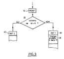
- FIG. 3 shows another embodiment of the invention.
- the program described above behaves as follows: when the reset pulse is associated with a power-up of the system, the location M contains a value which is different from the value K, since by construction all the memory emptied during the previous system shutdown. The initialization by INIT1, corresponding to a power-up, is therefore carried out, then the value K is loaded into the location M.
- step 20 When, without intermediate powering down of the system, another reset pulse is applied to the RESET input, then it is noted in step 20 that the memory location M does indeed contain K, and the connection is therefore made to the subroutine INIT2 responsible for managing this second type of reset.
- the value K must be different from the value contained in the considered location M of the memory following the powering up of the system.
- this memory by construction, is completely filled with logical zeros during a power-up, it suffices in practice to choose a value K different from zeros, and of a completely arbitrary number of bits.
- the memory contains at power-up only logical levels "1”, it suffices to use for the value of K a word containing at least one logical zero, and in the limit a single bit at zero.
- the RAM memory contains during a power-up a random distribution of "0" and "1" logic, then it is necessary that K is in the form of a word having the greatest possible number of bits, in order to prevent accidentally the content of M at power-up being equal to the predetermined value K.
- the present invention has been described in an application in which it is sought to make a distinction between an awakening of the microprocessor by a power-up, an alarm clock for locking / unlocking remote accesses and an alarm clock for locking / unlocking accesses by key, it is understood that the invention applies to distinctions of types and natures entirely any; for example, the reset or interrupt pulse can be applied as part of a microprocessor learning a new remote control code, or else data exchange with an electronic injection computer of the motor, to which the microprocessor can be connected.
Landscapes
- Engineering & Computer Science (AREA)
- Theoretical Computer Science (AREA)
- Physics & Mathematics (AREA)
- General Engineering & Computer Science (AREA)
- General Physics & Mathematics (AREA)
- Power Sources (AREA)
- Microcomputers (AREA)
- Stored Programmes (AREA)
Applications Claiming Priority (2)
| Application Number | Priority Date | Filing Date | Title |
|---|---|---|---|
| FR9000344A FR2657181A1 (fr) | 1990-01-12 | 1990-01-12 | Procede et dispositif pour associer a la reception d'impulsions de reinitialisation par un microprocesseur l'acces a des sous-programmes differents. |
| FR9000344 | 1990-01-12 |
Publications (2)
| Publication Number | Publication Date |
|---|---|
| EP0437400A1 true EP0437400A1 (de) | 1991-07-17 |
| EP0437400B1 EP0437400B1 (de) | 1994-06-29 |
Family
ID=9392728
Family Applications (1)
| Application Number | Title | Priority Date | Filing Date |
|---|---|---|---|
| EP91400040A Expired - Lifetime EP0437400B1 (de) | 1990-01-12 | 1991-01-10 | Verfahren und Einrichtung zum Verknüpfen von Reinitialisierungsimpulsen für einen Mikroprozessor mit Zugriff zu verschiedenen Unterprogrammen |
Country Status (6)
| Country | Link |
|---|---|
| US (1) | US5386576A (de) |
| EP (1) | EP0437400B1 (de) |
| JP (1) | JPH04211817A (de) |
| DE (1) | DE69102658T2 (de) |
| ES (1) | ES2060309T3 (de) |
| FR (1) | FR2657181A1 (de) |
Cited By (2)
| Publication number | Priority date | Publication date | Assignee | Title |
|---|---|---|---|---|
| FR2726793A1 (fr) * | 1994-11-10 | 1996-05-15 | Mitsubishi Electric Corp | Appareil de commande pour vehicule |
| WO1999031568A1 (de) * | 1997-12-12 | 1999-06-24 | Leopold Kostal Gmbh & Co. Kg | Elektronische schaltungsandordnung zum beaufschlagen eines mikroprozessors mit weck- und aktionssignalen |
Families Citing this family (3)
| Publication number | Priority date | Publication date | Assignee | Title |
|---|---|---|---|---|
| JP3434934B2 (ja) * | 1995-06-07 | 2003-08-11 | 株式会社デンソー | ワイヤレス車両制御システム |
| US8051282B2 (en) * | 2008-04-02 | 2011-11-01 | S.C. Johnson & Son, Inc. | Low voltage reset determination and operational flow modification for microprocessor-controlled devices |
| EP2371108A1 (de) * | 2008-12-26 | 2011-10-05 | Thomson Licensing | Verfahren und vorrichtung zum konfigurieren von einrichtungen |
Citations (4)
| Publication number | Priority date | Publication date | Assignee | Title |
|---|---|---|---|---|
| EP0009862A1 (de) * | 1978-09-05 | 1980-04-16 | Motorola, Inc. | Programmierbare Betriebsartauswahl durch Rücksetzen und diese Auswahl verwendende Datenverarbeitungsanlage |
| DE3248680A1 (de) * | 1982-01-25 | 1983-09-22 | Tokyo Shibaura Denki K.K., Kawasaki | Microcomputer mit energiespar-betriebszustand |
| WO1989009957A1 (en) * | 1988-04-14 | 1989-10-19 | Robert Bosch Gmbh | Microcomputer with reset signal distinguishing means |
| FR2638867A1 (fr) * | 1988-11-04 | 1990-05-11 | Sgs Thomson Microelectronics | Procede et circuit de reinitialisation du fonctionnement d'un circuit |
Family Cites Families (13)
| Publication number | Priority date | Publication date | Assignee | Title |
|---|---|---|---|---|
| US4030073A (en) * | 1975-11-05 | 1977-06-14 | Digital Equipment Corporation | Initialization circuit for establishing initial operation of a digital computer |
| US4228502A (en) * | 1977-06-29 | 1980-10-14 | Hitachi, Ltd. | Electronic computer system |
| US4432049A (en) * | 1978-09-05 | 1984-02-14 | Pern Shaw | Programmable mode select by reset |
| US4427464A (en) * | 1981-12-31 | 1984-01-24 | Bell Telephone Laboratories, Incorporated | Liquid phase epitaxy |
| US4489394A (en) * | 1982-04-21 | 1984-12-18 | Zenith Electronics Corporation | Microprocessor power on reset system |
| US4590557A (en) * | 1983-09-12 | 1986-05-20 | Pitney Bowes Inc. | Method and apparatus for controlling software configurations in data processing systems |
| US4812677A (en) * | 1987-10-15 | 1989-03-14 | Motorola | Power supply control with false shut down protection |
| US5018062A (en) * | 1987-10-23 | 1991-05-21 | A.I. Architects, Inc. | Method and apparatus for overriding a ROM routine in response to a reset |
| US5073943A (en) * | 1988-12-27 | 1991-12-17 | Ford Motor Company | Automotive audio system having active controls in reduced power state |
| US4965550A (en) * | 1989-10-30 | 1990-10-23 | Chrysler Corporation | Automatic wake-up circuit arrangement for a single wire multiplex switch monitoring system |
| US5081586A (en) * | 1990-02-20 | 1992-01-14 | Eaton Corporation | Multiplexing of accessories in a vehicle |
| US5134580A (en) * | 1990-03-22 | 1992-07-28 | International Business Machines Corporation | Computer with capability to automatically initialize in a first operating system of choice and reinitialize in a second operating system without computer shutdown |
| US5159217A (en) * | 1991-07-29 | 1992-10-27 | National Semiconductor Corporation | Brownout and power-up reset signal generator |
-
1990
- 1990-01-12 FR FR9000344A patent/FR2657181A1/fr active Granted
-
1991
- 1991-01-10 EP EP91400040A patent/EP0437400B1/de not_active Expired - Lifetime
- 1991-01-10 DE DE69102658T patent/DE69102658T2/de not_active Expired - Fee Related
- 1991-01-10 ES ES91400040T patent/ES2060309T3/es not_active Expired - Lifetime
- 1991-01-11 JP JP3012544A patent/JPH04211817A/ja active Pending
-
1993
- 1993-04-19 US US08/049,051 patent/US5386576A/en not_active Expired - Fee Related
Patent Citations (4)
| Publication number | Priority date | Publication date | Assignee | Title |
|---|---|---|---|---|
| EP0009862A1 (de) * | 1978-09-05 | 1980-04-16 | Motorola, Inc. | Programmierbare Betriebsartauswahl durch Rücksetzen und diese Auswahl verwendende Datenverarbeitungsanlage |
| DE3248680A1 (de) * | 1982-01-25 | 1983-09-22 | Tokyo Shibaura Denki K.K., Kawasaki | Microcomputer mit energiespar-betriebszustand |
| WO1989009957A1 (en) * | 1988-04-14 | 1989-10-19 | Robert Bosch Gmbh | Microcomputer with reset signal distinguishing means |
| FR2638867A1 (fr) * | 1988-11-04 | 1990-05-11 | Sgs Thomson Microelectronics | Procede et circuit de reinitialisation du fonctionnement d'un circuit |
Cited By (2)
| Publication number | Priority date | Publication date | Assignee | Title |
|---|---|---|---|---|
| FR2726793A1 (fr) * | 1994-11-10 | 1996-05-15 | Mitsubishi Electric Corp | Appareil de commande pour vehicule |
| WO1999031568A1 (de) * | 1997-12-12 | 1999-06-24 | Leopold Kostal Gmbh & Co. Kg | Elektronische schaltungsandordnung zum beaufschlagen eines mikroprozessors mit weck- und aktionssignalen |
Also Published As
| Publication number | Publication date |
|---|---|
| EP0437400B1 (de) | 1994-06-29 |
| DE69102658D1 (de) | 1994-08-04 |
| ES2060309T3 (es) | 1994-11-16 |
| JPH04211817A (ja) | 1992-08-03 |
| DE69102658T2 (de) | 1994-10-13 |
| US5386576A (en) | 1995-01-31 |
| FR2657181A1 (fr) | 1991-07-19 |
| FR2657181B1 (de) | 1994-08-19 |
Similar Documents
| Publication | Publication Date | Title |
|---|---|---|
| EP0252812B1 (de) | Sicherheitseinrichtung, die die Funktion einer elektronischen Einrichtung nach der ersten Unterbrechung ihrer elektrischen Speisung unterbindet | |
| FR2675602A1 (fr) | Procede et dispositif de protection d'un systeme informatique. | |
| EP0368727A1 (de) | Sicherheitsanordnung gegen unbefugtes Aufspüren von geschützten Daten | |
| FR2606530A1 (fr) | Circuit integre pour la memorisation et le traitement d'informations de maniere confidentielle comportant un dispositif anti-fraude | |
| EP0437400B1 (de) | Verfahren und Einrichtung zum Verknüpfen von Reinitialisierungsimpulsen für einen Mikroprozessor mit Zugriff zu verschiedenen Unterprogrammen | |
| EP0735489B1 (de) | Verfahren zum Schützen nichtflüchtiger Speicherbereiche | |
| FR2720174A1 (fr) | Procédé pour tester le déroulement d'un programme d'instructions exécutées par un circuit intégré spécialisé, et circuit intégré spécialisé s'y rapportant. | |
| FR2819070A1 (fr) | Procede et dispositif de protection conte le piratage de circuits integres | |
| EP0884704B1 (de) | Beglaubigungsverfahren für integrierte Schaltung | |
| FR2528196A1 (fr) | Appareil de protection de programmes d'ordinateur | |
| FR2618926A1 (fr) | Dispositif a memoire de controle de l'utilisation d'un logiciel, du type cle | |
| EP0635789B1 (de) | Mikrokontroller Integrierteschaltung mit Festprogramm enthaltenden Festwertspeicher, Teststation und entsprechendes Herstellungsverfahren | |
| FR2513418A1 (fr) | Dispositif d'affichage avec compensation du temps de retard | |
| EP1020800B1 (de) | Mikroprozessor mit Schutzschaltungen zur Sicherung des Zugangs zu seinen Registern | |
| FR2752992A1 (fr) | Dispositif de protection de donnees memorisees | |
| FR2810438A1 (fr) | Circuit de detection d'usure | |
| FR2752993A1 (fr) | Dispositif de protection de donnees memorisees utilisant un circuit de temporisation | |
| EP1202181A1 (de) | Zugriffssteuerung zu einem integrierten Speicher mit einem Mikroprozessor | |
| EP1503288B1 (de) | Fehlererkennungszelle für integrierte Prozessoren | |
| EP0881768A1 (de) | System und Verfahren zur Filterung eines Impulssignals | |
| EP0685796A1 (de) | Anordnung zur Optimierung der Leistung eines Prozessors | |
| CA2297257A1 (fr) | Dispositif de gestion d'un clavier a touches | |
| EP0138709B1 (de) | Prüfung des Ladens von zum Serienparalleltyp gehörenden integrierten Schaltungen, mit von den Ausgabestufen getrenntem Laderegister | |
| EP0264325B1 (de) | Automat für das Kompatibelmachen eines Prozessors mit dem Bus eines anderen Prozessors | |
| EP0908828A1 (de) | Verteiltes Speicherzugriffsteuersystem und Verfahren |
Legal Events
| Date | Code | Title | Description |
|---|---|---|---|
| PUAI | Public reference made under article 153(3) epc to a published international application that has entered the european phase |
Free format text: ORIGINAL CODE: 0009012 |
|
| AK | Designated contracting states |
Kind code of ref document: A1 Designated state(s): DE ES GB IT |
|
| 17P | Request for examination filed |
Effective date: 19910923 |
|
| 17Q | First examination report despatched |
Effective date: 19930723 |
|
| GRAA | (expected) grant |
Free format text: ORIGINAL CODE: 0009210 |
|
| RAP1 | Party data changed (applicant data changed or rights of an application transferred) |
Owner name: VALEO SECURITE HABITACLE |
|
| AK | Designated contracting states |
Kind code of ref document: B1 Designated state(s): DE ES GB IT |
|
| REF | Corresponds to: |
Ref document number: 69102658 Country of ref document: DE Date of ref document: 19940804 |
|
| GBT | Gb: translation of ep patent filed (gb section 77(6)(a)/1977) |
Effective date: 19940802 |
|
| ITF | It: translation for a ep patent filed |
Owner name: SOCIETA' ITALIANA BREVETTI S.P.A. |
|
| REG | Reference to a national code |
Ref country code: ES Ref legal event code: FG2A Ref document number: 2060309 Country of ref document: ES Kind code of ref document: T3 |
|
| PLBE | No opposition filed within time limit |
Free format text: ORIGINAL CODE: 0009261 |
|
| STAA | Information on the status of an ep patent application or granted ep patent |
Free format text: STATUS: NO OPPOSITION FILED WITHIN TIME LIMIT |
|
| 26N | No opposition filed | ||
| ITTA | It: last paid annual fee | ||
| PGFP | Annual fee paid to national office [announced via postgrant information from national office to epo] |
Ref country code: GB Payment date: 19961223 Year of fee payment: 7 |
|
| PGFP | Annual fee paid to national office [announced via postgrant information from national office to epo] |
Ref country code: ES Payment date: 19970113 Year of fee payment: 7 |
|
| PGFP | Annual fee paid to national office [announced via postgrant information from national office to epo] |
Ref country code: DE Payment date: 19970321 Year of fee payment: 7 |
|
| PG25 | Lapsed in a contracting state [announced via postgrant information from national office to epo] |
Ref country code: GB Free format text: LAPSE BECAUSE OF NON-PAYMENT OF DUE FEES Effective date: 19980110 |
|
| PG25 | Lapsed in a contracting state [announced via postgrant information from national office to epo] |
Ref country code: ES Free format text: LAPSE BECAUSE OF NON-PAYMENT OF DUE FEES Effective date: 19980112 |
|
| GBPC | Gb: european patent ceased through non-payment of renewal fee |
Effective date: 19980110 |
|
| PG25 | Lapsed in a contracting state [announced via postgrant information from national office to epo] |
Ref country code: DE Free format text: LAPSE BECAUSE OF NON-PAYMENT OF DUE FEES Effective date: 19981001 |
|
| REG | Reference to a national code |
Ref country code: ES Ref legal event code: FD2A Effective date: 20000503 |
|
| PG25 | Lapsed in a contracting state [announced via postgrant information from national office to epo] |
Ref country code: IT Free format text: LAPSE BECAUSE OF NON-PAYMENT OF DUE FEES;WARNING: LAPSES OF ITALIAN PATENTS WITH EFFECTIVE DATE BEFORE 2007 MAY HAVE OCCURRED AT ANY TIME BEFORE 2007. THE CORRECT EFFECTIVE DATE MAY BE DIFFERENT FROM THE ONE RECORDED. Effective date: 20050110 |