EP0435527B1 - Kodierung eines Bildelementes - Google Patents
Kodierung eines Bildelementes Download PDFInfo
- Publication number
- EP0435527B1 EP0435527B1 EP90313637A EP90313637A EP0435527B1 EP 0435527 B1 EP0435527 B1 EP 0435527B1 EP 90313637 A EP90313637 A EP 90313637A EP 90313637 A EP90313637 A EP 90313637A EP 0435527 B1 EP0435527 B1 EP 0435527B1
- Authority
- EP
- European Patent Office
- Prior art keywords
- pixel
- value
- difference
- attribute
- color
- Prior art date
- Legal status (The legal status is an assumption and is not a legal conclusion. Google has not performed a legal analysis and makes no representation as to the accuracy of the status listed.)
- Expired - Lifetime
Links
Images

Classifications
-
- G—PHYSICS
- G09—EDUCATION; CRYPTOGRAPHY; DISPLAY; ADVERTISING; SEALS
- G09G—ARRANGEMENTS OR CIRCUITS FOR CONTROL OF INDICATING DEVICES USING STATIC MEANS TO PRESENT VARIABLE INFORMATION
- G09G5/00—Control arrangements or circuits for visual indicators common to cathode-ray tube indicators and other visual indicators
- G09G5/02—Control arrangements or circuits for visual indicators common to cathode-ray tube indicators and other visual indicators characterised by the way in which colour is displayed
Definitions
- This invention relates to picture element (pixel) encoding, and, more particularly, to apparatus and method for increasing the resolution of a display by reducing pixel quantization effects.
- a typical display such as may be used in combination with a real-time computer image generation (CIG) system
- CCG computer image generation
- an image of an object is presented to a viewer as a series of frames.
- rate at which a frame is updated may vary, it is customary to use a 30Hz update rate which corresponds to the update rate used for the NTSC television standard.
- raster lines having a predetermined number of pixels per line are generated in response to video information generated by the CIG system.
- Pixels are generally square or rectangular portions of the display and are arranged in a grid.
- the lines of the raster may be presented in either an interlaced or non-interlaced format.
- interlaced format two fields, each updated at say a 60Hz rate, are used for presenting the respective odd and even lines of the frame. That is, after the lines of the odd field have been displayed, the lines of the even field are displayed between appropriate lines of the odd field.
- non-interlaced format the lines of the frame are generally sequentially presented.
- the ultimate goal of a CIG system is to determine an attribute for an image to be displayed such as the color or shade of gray for monochrome system of each pixel of a display device, so that when each pixel is displayed with its assigned color value, the desired image is formed on the display device.
- Descriptors of image features are typically stored as polygons, or faces.
- a common sampling scheme which assigns the color of a polygon to any pixel whose center is covered by the polygon as determined by a view ray from the observer through the pixel center to the polygons in viewer space results in aliasing, which may be manifested by a flashing effect along edges within the image.
- One way to minimize aliasing is to super sample the pixel at subpixel locations. Each pixel is divided into a plurality of subpixels and the color of a polygon intercepted by a view ray passing through the center of the subpixel is assigned to the subpixel. After colors have been assigned to all subpixels, the color of the overall pixel may be determined, such as by averaging the colors of all subpixels of the pixel. Details of CIG systems for image processing may be found by refering to U.S.
- a continuum of colors may be displayed along a line of a raster subject to a restriction that color may not change faster than the bandwidth of the display device. For example, if a raster line contains 1024 pixels as supplied by the CIG system and the information from the CIG system is limited to changing only once for any pixel, then a color change, say from black to white or from white to black, in the space of less than one pixel cannot be displayed. However, generally there is no restriction placed on the display device as to where along the raster line a color change can occur, only a restriction on the rate or frequency of change.
- the modulation transfer function is an indication of the resolution of a display system, or an indication of the quality of the rendition of an image obtained from a predetermined input value used to generate the image.
- Resolution may be regarded as the ability of a system to detect and/or display spaced apart edges. The closer edges are that may still be accurately detected or displayed, the higher the resolution.
- white and black will be used as examples of contrasting colors throughout, wherein a color resulting from a combination of white and black is represented as shade of gray. It is to be understood that this invention is applicable to any colors including different intensities of the same color.
- a standard test for determining MTF involves moving, or sampling, a bar pattern of alternating contrasting colors, wherein a bar of the pattern is about 1 to about 1.25 pixels wide, across the pixel grid and displaying the result. If the contrasting colors are say black and white, then a display of any color different from black or white, such as a shade of gray, represents a loss of information and a corresponding MTF of less than 100 percent.
- apparatus for increasing the resolution of an image display comprises difference means for producing a difference signal representative of the difference value between an attribute, such as color, of one portion of a pixel to be displayed and the attribute of another mutually exclusive portion of the pixel to be displayed, comparator means, coupled to the difference means, for determining in response to receipt of the difference signal if the difference value is greater than or equal to a predetermined threshold, and processor means, coupled to the comparator means, for assigning a first value of the attribute to said one portion of the pixel and a second value of the attribute to said another portion of the pixel when the difference value is greater than or equal to the threshold and for assigning a third value of the attribute to the entire pixel when the difference is less than the threshold and storage means, coupled to the processor means, for storing the first and second attribute value of said one and said another portions of the pixel when assigned and for storing the third attribute value when assigned wherein the characteristics of the pixel to be displayed during a pixel interval are changed during the pixel interval
- the first, second and third values of the attribute may be provided to a display for controlling the display characteristic of the pixel to be displayed. If the third value is assigned, the pixel to be displayed retains the third value throughout the pixel interval. If the first and second values are assigned to said one and said another portions of the pixel to be displayed, then the first value is retained for said one portion and after a transition within the pixel interval the second value is retained for said another portion.
- the first and second values of the attribute may be respective averages of the attribute for the corresponding said one and said another portion, or respective parts of said one and said another portion, such as may be determined by a computer image generation system.
- the apparatus may further include a respective plurality of difference means, comparator means and processor means for processing a respective plurality of components of the attribute, such as red, green and blue color components of a color attribute for forming a full color image at the display.
- the storage means may be bulk disk or random access memory (RAM), for storing the assigned first, second and third values of the attribute at logical locations corresponding to the pixel.
- RAM random access memory
- the apparatus may include selector means, such as a multiplexer, for selecting either the third value or the first value and the second value.
- selector means such as a multiplexer, for selecting either the third value or the first value and the second value.
- the method may further include representing the first value by a first data word having a first predetermined number of bits and representing the second value by a second data word having a second predetermined number of bits and representing the third value by a third data word having a third predetermined number of bits, wherein the sum of the second and third predetermined numbers of bits is less than or equal to the first predetermined number of bits.
- the second and third number of bits may be expressed as a respective mantissa and corresponding exponent.
- the color may be represented by Y (luminesce or luminance), I (in-phase chroma) and Q (quadrature chroma).
- the color may include first, second and third color components, such as red, green and blue
- the method may further include determining the difference between the first, second and third color components of said one portion of the pixel and the corresponding first, second and third color components of said another portion of the pixel, representing the pixel by a first value of each of the first, second and third color components when each difference is less than a corresponding predetermined threshold and represents said one portion by a corresponding second value of each of the first, second and third color components and said another portion of the pixel by a corresponding third value of each of the first, second and third color components when any difference is greater than or equal to the corresponding predetermined threshold.
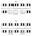
- Fig. 1 is a bar code pattern and resultant display in accordance with a previous computer image generation system.
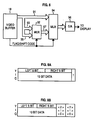
- Fig. 2A, 2B and 2C are block diagrams of a pixel encoder for a respective color component in accordance with the present invention.
- Fig. 3A is a pixel divided into subpixels in accordance with a previous computer image generation system.
- Fig. 3B is an encoded pixel in accordance with the present invention.
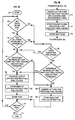
- Fig. 4A is a flow diagram for pixel encoding in accordance with an embodiment of the present invention.
- Fig. 4B is a modification of the flow diagram of Fig. 3A in accordance with another aspect of the present invention.
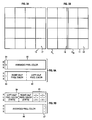
- Fig. 5A is a formatted pixel word in accordance with the encoding of Fig. 4A.
- Fig. 5B is a formatted pixel word in accordance with the encoding of Fig. 4B.
- Fig. 6 is a block diagram of video processing circuitry useful with the present invention.
- Fig. 7 is a bar code pattern and resultant display in accordance with the present invention.
- Figs. 8A and 8B are formatted pixel words in accordance with another aspect of the present invention.
- a test bar code pattern A and resultant display C in accordance with a previous computer image generation system are shown.
- Bar code pattern A is an alternating white and black pattern with each bar being one pixel wide.
- the short vertical lines transverse line B represent the beginning of each pixel and/or the ending of the previous pixel.
- Bar code pattern C represents what is displayed in response to the corresponding input pattern of A when pattern A is sampled at pixel boundaries indicated in B.
- the indication DG refers to dark gray, that is a mixture of white and black with more black than white
- the indication LT/G refers to light gray, that is a mixture of white and black with more white than black.
- Pattern A1 is aligned to start at a pixel edge and the resultant C1 pattern replicates the A1 pattern.
- pattern A is sequentially shifted through phases A2, A3, A4 and A5 to commence at a respective one-quarter pixel later than the previous phase, it is noted that the corresponding phases C2, C3, C4 and C5 of displayed pattern C do not necessarily replicate the pattern of corresponding phases A2, A3, A4 and A5 of input pattern A.
- phase C3 wherein phase A3 is shifted so that the bars of phase A3 are centered on pixel boundaries indicated in row B, no unmodified original information is displayed.
- FIGs. 2A, 2B and 2C block diagrams of a pixel encoder for a respective color component in accordance with the present invention are shown.
- the colors red (R), green (G) and blue (B) are chosen herein.
- Pixel encoder 10 for one color component, such as red (R) is shown in detail, it being understood that pixel encoders 20 and 30 for other color components, such as green (G) and blue (B) respectively, may be analogously configured.
- Application of the present invention is not limited to particular colors or to the number of colors or color components.
- Pixel encoder 10 includes a summer 12 having a non-inverting input constituting an input of encoder 10 and an inverting input constituting another input of encoder 10, an adjustable or adaptive threshold detector 14 having an input connected to the output of summer 12 for receiving a difference signal e, therefrom, a processor/encoder 16 having a pair of inputs each connected to a respective input of encoder 10 and respective outputs connected to respective inputs of video buffer 18 for providing a pixel average color signal, an encoder pixel color descriptor signal (R′ L + R′ R ) and a flag/shift code signal thereto.
- the corresponding outputs from processor/encoder of G circuitry 20 and B circuitry 30 may be connected to respective portions of video buffer 18 or to a respective separate video buffer as desired.
- each of the R, G and B color components for a pixel are typically independently processed in parallel by the CIG system.
- pixel encoders 10, 20 and 30 will be operating on red, green and blue color components, respectively, for the same pixel.
- an encode signal is supplied from another output of threshold detector 14, which also constitutes another output of pixel encoder 10, to each of G pixel encoder 20 and B pixel encoder 30 for signifying when an encode operation is detected by pixel encoder 20 as explained in detail below.
- a pixel 15 that is subdivided into subpixels 17 is shown.
- the color value of the red color component of each subpixel 17 of pixel 15 is added and a resulting average for the red color component is assigned as the red color of pixel 15.
- the blue and green components are processed analogously.
- the assigned red, green and blue color values are ultimately supplied to a display device for generating an image.
- the value of each color component may be adequately represented by a 12-bit word.
- a pixel 11 also includes subpixels 13. However, in accordance with the present embodiment pixel 11 is also logically divided into right and left halves as shown by vertical lines 19. Lines 19 are shown as closely spaced lines to avoid confusion with the boundary lines of subpixels 13, it being understood that a single line may be used to indicate central vertical divider 19.
- pixel 11 as shown is oriented so that vertical lines 19 are transverse a raster line of the display.
- the red color component for each subpixel 13 or the left half of pixel 11 is designated R L and the red color component for each subpixel 13 of the right half of pixel 11 is designated R R .
- the green (G) and blue (B) color components are designated by an appropriate left (L) and right (R) subscript.
- the present invention is not dependent on the number of subpixels 13 into which pixel 11 is divided. In fact, in order to achieve benefits of the present invention, it is not necessary that pixel 11 have any subpixels, in which case the value of color components R L and R R are also the value of the overall color component of the left and right half, respectively, of pixel 11.
- the value of right half red color component R R of subpixels 13 of pixel 11 is supplied to the inverting input of summer 12 and the value of left half red color component R L of subpixels 13 of pixel 11 is provided to the non-inverting input of summer 12.
- Color components R L and R R may each be represented by a 12-bit word for each subpixel 13 and pixel 11 and supplied from a CIG system.
- Left half red component R L may be the average value of the red color component of each subpixel 13 of the left half of pixel 11
- right half red color component R R may be the average value of the red color component of each subpixel 13 of the right half of pixel 11.
- Right color component R R and left color component R L representing the brightness or intensity of the red color component of the corresponding portion of pixel 11, are algebraically combined by summer 12 and the difference signal e is supplied to threshold detector 14.
- Difference signal e represents the difference in color intensity between the right and left halves of pixel 11. If the value of difference signal e is less than a predetermined adjustable, or adaptive, threshold as determined by threshold detector 14, which may include a digital comparator, a threshold signal that is supplied to processor/encoder 16 is set to a no encode state.
- right color component R R and left color component R L available at respective inputs of processor/encoder 16 are averaged by processor/encoder 16 and the resulting average value is supplied as the average red color signal whose value is to be stored at the logical red location in video buffer 18 corresponding to pixel 11.
- the threshold signal is set to an encode state.
- right color component R R and left color component R L are modified or encoded by processor/encoder 16 and are supplied in a modified state as the R′ R and R′ L signal to video buffer 18 for storage at the logical location corresponding to pixel 11.
- a flag/shift code signal which is supplied by processor/encoder 16 to video buffer 18 is also set in this case to indicate that the R′ R and R′ L color component signals have been provided in an encoded, or divided, format.
- threshold detector 14 determines that difference signal e is greater than the predetermined threshold, then threshold detector sets the encode signal, which is provided to corresponding other color pixel encode circuitry 20 and 30, to indicate that an encode operation has been detected by pixel encoder 10. Receipt of an encode signal indicating that one pixel encoder has detected that an encode operation is to be performed, may be used to force the pixel encoder receiving such encode signal to encode the corresponding right and left half pixel color components, irrespective of whether the difference between the right and left half pixel component values has exceeded the corresponding predetermined threshold. If the size of memory storage is desired to be expanded for words having the same resolution as shown with respect to Figs. 4A, 4B, 5A and 5B below to accommodate an individual shift code for each color, or the resolution of a word reduced to accommodate the individual shift code without expanding existing memory, then it is not necessary to use the encode signal for forcing encoding.
- FIG. 4A a flow diagram for pixel encoding in accordance with an embodiment of the present invention is shown.
- a general purpose computer such as one conventionally used in CIG systems may be programmed for performing the steps required.
- a program begins by executing step 52 to determine if there are any edges of faces within the pixel.
- step 52 is performed because there may be cases where the difference in intensity between the right and left half of the pixel exceeds the threshold and yet no vertical or substantially vertical edge of a face passes through the pixel.
- This may be a hole in an object which is created by the CIG system using appropriate translucency coding, wherein the color seen through the hole is different from the color of the object.
- Substantially vertical as used herein means that the angle of the edge is greater than a predetermined angle from the horizontal if the edge were to be displayed and includes a vertical edge.
- step 54 determines if all edges within the pixel are within a predetermined limit of a horizontal line through the pixel.
- Dividing a pixel 16 by vertical lines 19 for processing the pixel color components in right and left halves as shown in Fig. 3B is intended to increase horizontal resolution along a raster line. If an edge through pixel 16 is horizontal or substantially horizontal as determined by the predetermined limit, then the color contribution of the polygon of which the edge forms a part of the perimeter to the right and left halves of pixel 16 would be expected to be equal or substantially equal, respectively, and whose effect would be expected to be negated when processed by summer 12 (Fig. 2A).
- step 56 is executed to determine if the difference between the left and right half color component of the pixel is greater than a predetermined threshold. If the difference is greater than the threshold when step 56 is performed then the YES path is followed to step 58.
- Performance of step 58 modifies the right R R and left R L color component descriptors of the pixel such as by truncating the least significant bits of the right R R and left R L descriptors to form modified color component descriptors R′ R and R′ L′ respectively.
- Step 60 is then executed to store the remaining MSB's of the data word describing the left and right half of the pixel, respectively, and performance of step 62 stores a flag sign to indicate that the color components of the pixel have been stored as left and right half descriptors.
- a flag bit 83 of data word 82 is also set to a logical one indicating that the color component descriptors of the pixel have been stored as left and right half color portions.
- data word 82 can be stored in the same memory location as would have been the prior overall color component of the pixel, thereby avoiding the need for storage hardware memory allocation modification while achieving benefits of the present invention.
- step 64 for determining if there is another pixel to be processed. If there is no other pixel to be processed when step 64 is performed then the program follows the NO path to step 70. Execution of step 70 ends the program until it is restarted by performance of step 50.
- step 52 If there are no edges within the pixel when step 52 is executed then the program follows the NO path to step 55, or if all edges with the pixel are within the predetermined limit of horizontal when step 54 is performed then the program follows the YES path to step 55.
- step 55 determines if all faces entirely cover the pixel and further if all such faces are opaque. If both conditions are true when step 55 is executed then the program follows the YES path to step 56, otherwise the program follows the NO path to step 57.
- Performance of step 57 determines if the difference between the left and right half color component values is greater than a predetermined threshold. If the difference exceeds the threshold when step 57 is performed the program follows the YES path to step 58.
- step 57 If the difference is not greater than the threshold when step 57 is performed then the program follows the NO path to step 66, or if the difference between the left and right half color components of the pixel are not greater than the predetermined threshold when step 56 is executed then the program follows the NO path to step 66.
- step 66 algebraically combines the values of the left half color component R L and the right half color component R R of the pixel and determines an average value.
- the program proceeds to step 68 whose performance stores the average value of the color component of the pixel along with a flag bit 81 set to a logical zero to indicate that the stored pixel component color information is stored as an average value, for the entire pixel as shown in word format 80 of Fig. 5A.
- the average value stored by execution of step 68 may be an 11-bit word with one bit reserved for the flag bit.
- average pixel color component information can be stored without need of modifying existing storage hardware memory allocation.
- step 64 the program proceeds to step 64. If execution of step 64 indicates that there is another pixel to be processed then the program follows the YES path to step 52 and the next pixel is processed as described above.
- the threshold of step 56 is expected to be relatively low as the program arrives at step 56 directly from step 54 and is expected to be the same or slightly higher if the program arrives at step 56 directly from step 55.
- the threshold of step 57 is expected to be relatively high and greater than either threshold encountered at step 56. In any event, thresholds may be adjusted without undue experimentation to provide an optimum display as viewed by an observer.
- step 72 encodes the left half and the right half pixel color component information into a floating point format having a respective mantissa and a shift code, or exponent.
- Performance of step 74 stores the encoded values or mantissas for the left and right color components and execution of step 76 stores the left and right shift code for the corresponding mantissa. The program then proceeds to step 64 for processing as described above.
- the mantissa is selected as the five most significant bit positions starting with the bit position of the color component data word having the fewest MSB leading zeros until a logical one is encountered.
- the 12-bit right red data word has four MSB leading zeros and a logical one in the fifth MSB position
- the 12-bit right green data word has five MSB leading zeros and a logical one in the sixth MSB position
- the 12-bit right blue data word has six MSB leading zeros and a logical one in the seventh MSB position
- the shift code for the modified right red data word would be four or 100 (binary) for the four leading zeros of the right red data word, and the mantissa of the modified right red data word would be the value of the next five data bit positions, that is bit 5 through 9 of the right red data word.
- the mantissa for the right green and blue modified data words would be the value of data bit positions 5 through 9 of the green and blue data words, respectively, whereas the shift code for each of the modified green and blue data words would still be four.
- the mantissa for each modified right color component is stored in the format 84 illustrated in Fig. 5B.
- the shift code bit values for the left and right columns of shift code 85 are indicated by the power of two or exponent within the angle brackets ⁇ >.
- ⁇ o> represents 2 o or one's position
- ⁇ 1> represents 21 or two's position
- ⁇ 2> represents 22 or four's position.
- the right-hand column of shift code 85 represents the shift code for the right half mantissa
- the left-hand column of shift code 85 represents the shift code for the left half mantissa.
- the shift code was four (binary 100)
- the right-hand column of shift code 85 would read 100 from top to bottom.
- steps 66 and 68 are executed as described above, except that execution of step 68 stores a shift code rather than a flag.
- the left and right half color components are combined and averaged and the resultant MSB are stored in the format 86 shown in Fig. 5B.
- the right shift code is stored as a binary 111 indicating that the associated data words represents an average color of the entire pixel.
- the present invention is not limited to using 12-bit words for pixel color component descriptors.
- the total number of bits used for the color component description of each portion, or half, of the pixel should be the maximum number which along with any bits needed for flagging and/or shift encoding permits storage using the same memory allocation without modification as was used prior to application of the present invention.
- the length of the data word descriptors for defining pixel color component contribution to the overall color of the pixel may be increased accordingly.
- the present invention is not limited by the word format selected. Any format which accurately conveys the information desired may be used.
- FIG. 6 a block diagram of video processing circuitry useful with the present embodiment is shown.
- the video processing circuitry includes a pair of multiplexers (MUX) 92 and 94 and a digital to analog (D/A) converter 96.
- An output of video buffer 18 having pixel color component data available thereat is connected via data path 91 to an input of multiplexer 94 and via data paths 93 and 95 to two inputs of multiplexer 92.
- Multiplexer 92 selects right pixel color information from data path 93 and left pixel color information from data path 95 in response to the status of the flag/shift code signal.
- Multiplexer 94 selects the average pixel color information from data path 91 or the right and left pixel color information from data path 97, which is available from the output of multiplexer 92, in response to the status of the flag/shift code signal.
- Corresponding pixel color information is provided to D/A converter 96 for ultimate display.
- the average pixel color information is selected by multiplexer 94, only one pixel color component value is supplied for display during each pixel interval.
- left and right pixel color information is selected by multiplexer 94, then two color values are supplied for display during each pixel interval. That is, at the display, the color value of a pixel being displayed is changed twice during a pixel interval, once at the beginning and once in the middle of the pixel interval in accordance with the present embodiment.
- the circuitry of Fig. 6 is used for one color component. Analogous circuitry may be used for each other color component with the appropriate color component information available from video buffer 18 or a corresponding video buffer if another one is used for the color component.
- a bar code test pattern and resultant display in accordance with the present embodiment is shown.
- the bar code pattern of row A is the same pattern as was shown in Row A of Fig. 1.
- the short transverse lines across row B represent the beginning or end of a pixel interval.
- the present invention is not limited to dividing a pixel in half. Division into thirds, quarters or other portions with color component intensity comparisons performed between contiguous portions may be used subject to practical limitations such as processing time available for maintaining real time image generation.
- FIGs. 8A and 8B formatted pixel words in accordance with another aspect of the present invention are shown.
- the pixel word format shown in Figs. 8A and 8B may be used in systems employing YIQ color processing wherein Y represents color luminesce (intensity), and I and Q represent in-phase and quadrature chroma, respectively. Inasmuch as all intensity information is encoded into the Y component, only the difference between the Y component values is necessary for determining whether to provide an overall or average Y component value for the entire pixel, or whether to provide individual portions, such as left half and right half information, along with the appropriate flag or shift code.
- the Y component may be processed analogously to the red color component described above with respect to the flow diagram of Fig. 4A or Fig. 4B.
- step 58 indicates that truncation is appropriate then the word format of Fig. 8A, which is analogous to format 82 of Fig. 5A, may be used.
- step 72 indicates that encoding is appropriate then the word format of Fig. 8B, which is analogous to format 84 of Fig. 5B, may be used.
Landscapes
- Engineering & Computer Science (AREA)
- Physics & Mathematics (AREA)
- Computer Hardware Design (AREA)
- General Physics & Mathematics (AREA)
- Theoretical Computer Science (AREA)
- Controls And Circuits For Display Device (AREA)
- Image Processing (AREA)
- Picture Signal Circuits (AREA)
- Transforming Electric Information Into Light Information (AREA)
- Television Systems (AREA)
- Processing Of Color Television Signals (AREA)
- Editing Of Facsimile Originals (AREA)
Claims (15)
- Einrichtung zum Vergrößern der Auflösung eines abzubildenden Bildes, enthaltend:
eine erste Differenzeinrichtung (12) zum Erzeugen eines ersten Differenzsignals, das eine erste Differenz zwischen einem Attribut von einem Teil von einem abzubildenden Pixel und dem Attribut von einem anderen, sich wechselseitig ausschließenden Teil von einem abzubildenden Pixel darstellt,
eine erste Komparatoreinrichtung (14), die mit der ersten Differenzeinrichtung (12) verbunden ist, um bei Empfang des ersten Differenzsignals zu ermitteln, ob die erste Differenz größer als oder gleich einem ersten vorbestimmten Schwellenwert ist,
eine erste Prozessoreinrichtung (16), die mit der ersten Komparatoreinrichtung (14) verbunden ist, zum Zuordnen eines ersten Wertes des Attributes zu dem einen Teil des Pixels und eines zweiten Wertes des Attributes zu einem anderen Teil des Pixels, wenn die erste Differenz größer als oder gleich dem ersten vorbestimmten Schwellenwert ist, und zum Zuordnen eines dritten Wertes des Attributes zu dem gesamten Pixel, wenn die erste Differenz kleiner als der erste vorbestimmte Schwellenwert ist, und
eine Speichereinrichtung (18), die mit der ersten Prozessoreinrichtung (16) verbunden ist, zum Speichern des ersten und zweiten Attributwertes von dem einen und dem anderen Teil des Pixels, wenn sie zugeordnet sind, und zum Speichern des dritten Attributwertes, wenn er zugeordnet ist,
wobei die Charakteristiken des Pixels, das während eines Pixelintervalls abzubilden ist, während des Pixelintervalls bei den ersten und zweiten Attributwerten, wenn sie zugeordnet sind, verändert werden. - Einrichtung nach Anspruch 1, wobei das Attribut Farbe des Pixels ist.
- Einrichtung nach Anspruch 1 oder 2, wobei die Komparatoreinrichtung (14) einen einstellbaren Schwellenwertdetektor aufweist.
- Einrichtung nach Anspruch 1, 2 oder 3, wobei der dritte Wert durch ein Datenwort dargestellt ist, das eine vorbestimmte Anzahl von Bits aufweist, und die ersten und zweiten Werte jeweils durch einen entsprechenden gleichen Teil von einem anderen Datenwort dargestellt sind, wobei die Anzahl von Bits des anderen Datenwortes kleiner als oder gleich der vorbestimmten Anzahl von Bits ist.
- Einrichtung nach Anspruch 4, wobei die entsprechenden gleichen Teile jeweils eine Mantisse darstellen und das andere Datenwort ferner einen ansprechenden Exponenten für jede Mantisse aufweist.
- Einrichtung nach Anspruch 2, wobei das Attribut rote, grüne und blaue Farbkomponenten aufweist, wobei die erste Differenzeinrichtung, die erste Komparatoreinrichtung, die erste Prozessoreinrichtung und die Speichereinrichtung auf die rote Komponente des Attributs ansprechen, wobei die Einrichtung ferner enthält:
eine zweite Differenzeinrichtung (12) zum Erzeugen eines zweiten Differenzsignals, das eine Differenz zwischen der grünen Komponente des einen Teils des Pixels und der grünen Komponenten von dem anderen Teil des Pixels darstellt,
eine zweite Komparatoreinrichtung (14), die mit der zweiten Differenzeinrichtung (12) verbunden ist, um bei Empfang des zweiten Differenzsignals zu ermitteln, ob die zweite Differenz größer als oder gleich einem zweiten vorbestimmten Schwellenwert ist,
eine zweite Prozessoreinrichtung (16), die mit der zweiten Komparatoreinrichtung (14) verbunden ist, zum Zuordnen eines ersten Wertes der grünen Komponente zu dem einen Teil und eines zweiten Wertes der grünen Komponente zu dem anderen Teil des Pixels, wenn die zweite Differenz größer als oder gleich dem zweiten vorbestimmten Schwellenwert ist, und zum Zuordnen eines dritten Wertes der grünen Farbkomponente zu dem gesamten Pixel, wenn die zweite Differenz kleiner als der zweite vorbestimmte Schwellenwert ist,
eine dritte Differenzeinrichtung (12) zum Erzeugen eines dritten Differenzsignals, das eine Differenz zwischen der blauen Komponente von dem einen Teil des Pixels und der blauen Komponente von dem anderen Teil des Pixels darstellt,
eine dritte Komparatoreinrichtung (14), die mit der dritten Differenzeinrichtung (12) verbunden ist, um bei Empfang des dritten Differenzsignals zu ermitteln, ob die dritte Differenz größer als oder gleich einem dritten vorbestimmten Schwellenwert ist, und
eine dritte Prozessoreinrichtung (16), die mit der dritten Komparatoreinrichtung (12) verbunden ist, zum Zuordnen eines ersten Wertes der blauen Komponente zu dem einen Teil und eines zweiten Wertes der blauen Komponente zu dem anderen Teil des Pixels, wenn die dritte Differenz größer als oder gleich dem dritten vorbestimmten Schwellenwert ist, und zum Zuordnen eines dritten Wertes der blauen Komponente zu dem gesamten Pixel, wenn die dritte Differenz kleiner als der zweite vorbestimmte Schwellenwert ist, wobei
die Speichereinrichtung (18) weiterhin mit den zweiten und dritten Prozessoreinrichtungen (16) verbunden ist und den ersten und zweiten Wert der grünen Komponente und den ersten und zweiten Wert der blauen Komponente von dem einen und dem anderen Teil des Pixels speichert, wenn sie zugeordnet sind, und den dritten Wert von den grünen und blauen Komponenten des Pixels speichert, wenn er zugeordnet ist. - Einrichtung nach einem der vorstehenden Ansprüche, ferner enthaltend:
eine erste Wähleinrichtung (92, 94), die mit der Speichereinrichtung (18) verbunden ist, um zur Bildgebung bei der ersten Differenz entweder den ersten und zweiten Wert von dem einen und dem anderen Teil des Pixels oder den dritten Wert abzubilden. - Einrichtung nach Anspruch 2, wobei die Farbe in Größen von Y (Luminanz), I (gleichphasige Chrominanz) und Q (Quadraturchrominanz) ausgedrückt ist.
- Einrichtung nach einem der vorstehenden Ansprüche, wobei der eine Teil des Pixels die rechte Hälfte des Pixels ist und wobei der andere Teil des Pixels die linke Hälfte des Pixels ist.
- Verfahren zum Vergrößern der Auflösung eines abzubildenden Bildes, wobei das Bild aus Pixeln gebildet ist und jedes Pixel ein entsprechendes, zugeordnetes Attribut und ein entsprechendes Pixelintervall aufweist, enthaltend:
Ermitteln (56) der Differenz zwischen dem Attribut von dem einen Teil des Pixels und dem Attribut von einem anderen, sich wechselseitig ausschließenden Teil des Pixels,
Darstellen (66, 68) des Pixels durch einen ersten Wert des Attributs, wenn die Differenz kleiner als ein vorbestimmter Schwellenwert ist,
Darstellen (58, 60, 62, 72, 74, 76) des einen Teils durch einen zweiten Wert des Attributs und eines anderen Teils des Pixels durch einen dritten Wert des Attributs, wenn die Differenz größer als oder gleich dem vorbestimmten Schwellenwert ist, wobei das dem Pixel zugeordnete Attribut auf dem zweiten Wert für den einen Teil und auf dem dritten Wert für den anderen Teil ist, wodurch der Wert des dem Pixel zugeordneten Attributs sich während des Pixelintervalls ändern kann zur Herbeiführung einer erhöhten Auflösung. - Verfahren nach Anspruch 10, wobei der erste Wert durch ein erstes Datenwort dargestellt wird, das eine erste vorbestimmte Anzahl von Bits aufweist, wobei der Darstellungsschritt enthält:
Darstellen des zweiten Wertes durch ein zweites Datenwort, das eine zweite vorbestimmte Anzahl von Bits aufweist,
Darstellen des dritten Wertes durch ein drittes Datenwort, das eine dritte vorbestimmte Anzahl von Bits aufweist, wobei die Summe der zweiten und dritten vorbestimmten Bitzahlen kleiner als oder gleich der ersten vorbestimmten Bitzahl ist. - Verfahren nach Anspruch 11, ferner enthaltend:
Ausdrücken des zweiten Wertes unter Verwendung einer Mantisse und eines ersten entsprechenden Exponenten,
Ausdrücken des dritten Wertes unter Verwendung einer Mantisse und eines zweiten entsprechenden Exponenten. - Verfahren nach Anspruch 10, 11 oder 12, wobei das Attribut Farbe ist und die Farbe eine erste, zweite und dritte Farbkomponente enthält, wobei das Verfahren ferner enthält:
Ermitteln der Differenz zwischen den ersten, zweiten und dritten Farbkomponenten von dem einen Teil des Pixels und der entsprechenden ersten, zweiten und dritten Farbkomponenten von dem anderen Teil des Pixels,
Darstellen des gesamten Pixels durch einen entsprechenden ersten Wert von jeder der ersten, zweiten und dritten Farbkomponenten, wenn jede Differenz kleiner als ein entsprechender vorbestimmter Schwellenwert ist,
Darstellen des einen Teils von dem Pixel durch einen entsprechenden zweiten Wert von jeder der ersten, zweiten und dritten Farbkomponenten, und des anderen Teils von dem Pixel durch einen entsprechenden dritten Wert von jeder der ersten, zweiten und dritten Farbkomponenten, wenn irgendeine Differenz größer als oder gleich dem entsprechenden vorbestimmter Schwellenwert ist. - Verfahren nach Anspruch 13, wobei die ersten, zweiten und dritten Farbkomponenten rot, grün bzw. blau aufweisen.
- Verfahren nach Anspruch 10, wobei das Attribut die Farbe des Pixels ist und durch Y (Luminanz), I (gleichphasige Chrominanz) und Q (Quadraturchrominanz) dargestellt wird.
Applications Claiming Priority (2)
| Application Number | Priority Date | Filing Date | Title |
|---|---|---|---|
| US457876 | 1989-12-27 | ||
| US07/457,876 US5126726A (en) | 1989-12-27 | 1989-12-27 | Picture element encoding |
Publications (2)
| Publication Number | Publication Date |
|---|---|
| EP0435527A1 EP0435527A1 (de) | 1991-07-03 |
| EP0435527B1 true EP0435527B1 (de) | 1995-03-22 |
Family
ID=23818423
Family Applications (1)
| Application Number | Title | Priority Date | Filing Date |
|---|---|---|---|
| EP90313637A Expired - Lifetime EP0435527B1 (de) | 1989-12-27 | 1990-12-14 | Kodierung eines Bildelementes |
Country Status (5)
| Country | Link |
|---|---|
| US (1) | US5126726A (de) |
| EP (1) | EP0435527B1 (de) |
| JP (1) | JP2996310B2 (de) |
| DE (1) | DE69018046T2 (de) |
| IL (1) | IL96622A (de) |
Families Citing this family (42)
| Publication number | Priority date | Publication date | Assignee | Title |
|---|---|---|---|---|
| US5299308A (en) * | 1990-02-28 | 1994-03-29 | Ricoh Company, Ltd. | Graphic data processing apparatus for producing a tone for an edge pixel and reducing aliasing effects |
| US5867142A (en) * | 1991-11-25 | 1999-02-02 | Xerox Corporation | System and method for processing an image having edges |
| US5276532A (en) * | 1991-11-26 | 1994-01-04 | Xerox Corporation | Split-level frame buffer |
| US5598184A (en) * | 1992-03-27 | 1997-01-28 | Hewlett-Packard Company | Method and apparatus for improved color recovery in a computer graphics system |
| US5724475A (en) * | 1995-05-18 | 1998-03-03 | Kirsten; Jeff P. | Compressed digital video reload and playback system |
| TW316965B (de) * | 1995-10-31 | 1997-10-01 | Cirrus Logic Inc | |
| US6314140B1 (en) * | 1995-12-28 | 2001-11-06 | Lucent Technologies Inc. | Dynamic video focus control |
| US6108633A (en) * | 1996-05-03 | 2000-08-22 | Lsi Logic Corporation | Audio decoder core constants ROM optimization |
| US5818532A (en) * | 1996-05-03 | 1998-10-06 | Lsi Logic Corporation | Micro architecture of video core for MPEG-2 decoder |
| US5845249A (en) | 1996-05-03 | 1998-12-01 | Lsi Logic Corporation | Microarchitecture of audio core for an MPEG-2 and AC-3 decoder |
| US5870310A (en) * | 1996-05-03 | 1999-02-09 | Lsi Logic Corporation | Method and apparatus for designing re-usable core interface shells |
| US6430533B1 (en) | 1996-05-03 | 2002-08-06 | Lsi Logic Corporation | Audio decoder core MPEG-1/MPEG-2/AC-3 functional algorithm partitioning and implementation |
| US5793386A (en) * | 1996-06-28 | 1998-08-11 | S3 Incorporated | Register set reordering for a graphics processor based upon the type of primitive to be rendered |
| US5936635A (en) * | 1996-06-28 | 1999-08-10 | Cirrus Logic, Inc. | System and method of rendering polygons into a pixel grid |
| US5828382A (en) * | 1996-08-02 | 1998-10-27 | Cirrus Logic, Inc. | Apparatus for dynamic XY tiled texture caching |
| US5875295A (en) * | 1996-09-30 | 1999-02-23 | S3 Incorporated | Instruction format for ensuring safe execution of display list |
| US6348917B1 (en) | 1996-09-30 | 2002-02-19 | Cirrus Logic, Inc | Dynamic switching of texture mip-maps based on depth |
| US5987582A (en) * | 1996-09-30 | 1999-11-16 | Cirrus Logic, Inc. | Method of obtaining a buffer contiguous memory and building a page table that is accessible by a peripheral graphics device |
| US5986663A (en) * | 1997-10-10 | 1999-11-16 | Cirrus Logic, Inc. | Auto level of detail-based MIP mapping in a graphics processor |
| US6157386A (en) * | 1997-10-10 | 2000-12-05 | Cirrus Logic, Inc | MIP map blending in a graphics processor |
| US6333746B1 (en) | 1996-12-30 | 2001-12-25 | Cirrus Logic, Inc. | Auto level of detail texture mapping for a software graphics engine |
| US5844576A (en) * | 1996-12-30 | 1998-12-01 | Cirrus Logic, Inc. | Tiled linear host texture storage |
| US5835097A (en) * | 1996-12-30 | 1998-11-10 | Cirrus Logic, Inc. | Non-homogenous second order perspective texture mapping using linear interpolation parameters |
| US5841442A (en) * | 1996-12-30 | 1998-11-24 | Cirrus Logic, Inc. | Method for computing parameters used in a non-homogeneous second order perspective texture mapping process using interpolation |
| US6088016A (en) * | 1996-12-30 | 2000-07-11 | S3 Incorporated | Dithering method and apparatus using ramp probability logic |
| US6052127A (en) * | 1996-12-30 | 2000-04-18 | Cirrus Logic, Inc. | Circuit for determining non-homogenous second order perspective texture mapping coordinates using linear interpolation |
| US5977983A (en) * | 1997-02-20 | 1999-11-02 | S3 Incorporated | Method and apparatus for adjusting graphics processing procedures based on a selectable speed/quality gauge |
| US5929869A (en) * | 1997-03-05 | 1999-07-27 | Cirrus Logic, Inc. | Texture map storage with UV remapping |
| US6072508A (en) * | 1997-03-14 | 2000-06-06 | S3 Incorporated | Method and apparatus for shortening display list instructions |
| US6028613A (en) * | 1997-03-20 | 2000-02-22 | S3 Incorporated | Method and apparatus for programming a graphics subsystem register set |
| US5949421A (en) * | 1997-03-31 | 1999-09-07 | Cirrus Logic, Inc. | Method and system for efficient register sorting for three dimensional graphics |
| US6130674A (en) * | 1997-03-31 | 2000-10-10 | Cirrus Logic, Inc. | Dynamically selectable texture filter for computer graphics |
| US5978895A (en) * | 1997-04-04 | 1999-11-02 | Cirrus Logic, Inc. | Method for speeding mathematical operations in a processor core |
| US5835104A (en) * | 1997-04-23 | 1998-11-10 | S3 Incorporated | Variable band size compositing buffer method and apparatus |
| US5940090A (en) * | 1997-05-07 | 1999-08-17 | Cirrus Logic, Inc. | Method and apparatus for internally caching the minimum and maximum XY pixel address values in a graphics subsystem |
| US6266753B1 (en) | 1997-07-10 | 2001-07-24 | Cirrus Logic, Inc. | Memory manager for multi-media apparatus and method therefor |
| US6181347B1 (en) | 1997-09-17 | 2001-01-30 | Cirrus Logic, Inc. | Selectable mode smoothing texture filter for computer graphics |
| US6054993A (en) * | 1997-09-17 | 2000-04-25 | Cirrus Logic, Inc. | Chroma-keyed specular texture mapping in a graphics processor |
| US6002409A (en) * | 1997-10-29 | 1999-12-14 | Cirrus Logic, Inc. | Arbitration for shared graphics processing resources |
| US6259455B1 (en) | 1998-06-30 | 2001-07-10 | Cirrus Logic, Inc. | Method and apparatus for applying specular highlighting with specular components included with texture maps |
| US6252606B1 (en) | 1998-06-30 | 2001-06-26 | Cirrus Logic, Inc. | Error correction in a graphics processor |
| CN104633948B (zh) * | 2015-02-26 | 2019-04-12 | 芜湖美的厨卫电器制造有限公司 | 显示装置、热水器及其加热参数的显示方法 |
Family Cites Families (9)
| Publication number | Priority date | Publication date | Assignee | Title |
|---|---|---|---|---|
| JPS5563173A (en) * | 1978-11-06 | 1980-05-13 | Ricoh Co Ltd | Picture signal processing system |
| US4720745A (en) * | 1983-06-22 | 1988-01-19 | Digivision, Inc. | Method and apparatus for enhancing video displays |
| JPS6145279A (ja) * | 1984-08-09 | 1986-03-05 | 株式会社東芝 | スム−ジング回路 |
| US4721943A (en) * | 1985-10-11 | 1988-01-26 | Tektronix, Inc. | Digital-to-analog converter for video application |
| US4849746A (en) * | 1986-04-07 | 1989-07-18 | Dubner Computer Systems, Inc. | Digital video generator |
| GB8700565D0 (en) * | 1987-01-12 | 1987-02-18 | Crosfield Electronics Ltd | Video image enhancement |
| JPH01113789A (ja) * | 1987-10-28 | 1989-05-02 | Hitachi Ltd | 中間調表示装置 |
| JPH02100575A (ja) * | 1988-10-07 | 1990-04-12 | Toshiba Corp | 画像処理装置 |
| US4908780A (en) * | 1988-10-14 | 1990-03-13 | Sun Microsystems, Inc. | Anti-aliasing raster operations utilizing sub-pixel crossing information to control pixel shading |
-
1989
- 1989-12-27 US US07/457,876 patent/US5126726A/en not_active Expired - Lifetime
-
1990
- 1990-11-22 JP JP2315695A patent/JP2996310B2/ja not_active Expired - Fee Related
- 1990-12-10 IL IL9662290A patent/IL96622A/en not_active IP Right Cessation
- 1990-12-14 EP EP90313637A patent/EP0435527B1/de not_active Expired - Lifetime
- 1990-12-14 DE DE69018046T patent/DE69018046T2/de not_active Expired - Fee Related
Also Published As
| Publication number | Publication date |
|---|---|
| JPH03212685A (ja) | 1991-09-18 |
| JP2996310B2 (ja) | 1999-12-27 |
| EP0435527A1 (de) | 1991-07-03 |
| IL96622A (en) | 1994-06-24 |
| DE69018046T2 (de) | 1995-11-23 |
| US5126726A (en) | 1992-06-30 |
| DE69018046D1 (de) | 1995-04-27 |
| IL96622A0 (en) | 1991-09-16 |
Similar Documents
| Publication | Publication Date | Title |
|---|---|---|
| EP0435527B1 (de) | Kodierung eines Bildelementes | |
| US5227863A (en) | Programmable digital video processing system | |
| US5097257A (en) | Apparatus for providing output filtering from a frame buffer storing both video and graphics signals | |
| US6476824B1 (en) | Luminance resolution enhancement circuit and display apparatus using same | |
| EP0359080B1 (de) | Anzeigegerät mit einem geordneten Zittermuster | |
| US4991122A (en) | Weighted mapping of color value information onto a display screen | |
| US6023302A (en) | Blending of video images in a home communications terminal | |
| US5258747A (en) | Color image displaying system and method thereof | |
| EP0609980A2 (de) | Gerät und Verfahren zur Bewegungserfassung | |
| KR20000053089A (ko) | 디지탈 펄스 폭 변조 디스플레이 시스템에서 대역폭 및 프레임 버퍼 크기 감소 방법 | |
| US5663772A (en) | Gray-level image processing with weighting factors to reduce flicker | |
| WO1998029859A2 (en) | Improved dithering method and apparatus using ramp probability logic | |
| US6307498B1 (en) | Digital display unit of a computer system having an improved method and apparatus for sampling analog display signals | |
| EP0656616A1 (de) | Technik zur Steigerung des scheinbaren dynamischen Bereichs einer sichtbaren Anzeige | |
| EP0544510B1 (de) | Rasterpufferspeicher mit aufgeteiltem Pegel | |
| US5388168A (en) | Picture quality improving circuit using a cumulative histogram | |
| US6650337B2 (en) | Increasing color accuracy | |
| JPH05241550A (ja) | 色画像変換方法 | |
| US5894330A (en) | Adaptive anti-flicker method for VGA to TV data conversion | |
| CA2130164A1 (en) | Digital image processing apparatus | |
| US6088016A (en) | Dithering method and apparatus using ramp probability logic | |
| JPH08305330A (ja) | 誤差拡散方法・誤差拡散装置及び中間調処理方法 | |
| US4389672A (en) | Display of pseudo-gray scale picture signals on multilevel displays | |
| US6252578B1 (en) | Method for reducing flicker when displaying processed digital data on video displays having a low refresh rate | |
| US6911959B1 (en) | Low cost horizontal bar indicator system for on screen displays |
Legal Events
| Date | Code | Title | Description |
|---|---|---|---|
| PUAI | Public reference made under article 153(3) epc to a published international application that has entered the european phase |
Free format text: ORIGINAL CODE: 0009012 |
|
| AK | Designated contracting states |
Kind code of ref document: A1 Designated state(s): DE FR GB IT |
|
| 17P | Request for examination filed |
Effective date: 19911216 |
|
| 17Q | First examination report despatched |
Effective date: 19931014 |
|
| GRAA | (expected) grant |
Free format text: ORIGINAL CODE: 0009210 |
|
| AK | Designated contracting states |
Kind code of ref document: B1 Designated state(s): DE FR GB IT |
|
| REF | Corresponds to: |
Ref document number: 69018046 Country of ref document: DE Date of ref document: 19950427 |
|
| ET | Fr: translation filed | ||
| ITF | It: translation for a ep patent filed |
Owner name: SAIC BREVETTI S.R.L. |
|
| PLBE | No opposition filed within time limit |
Free format text: ORIGINAL CODE: 0009261 |
|
| STAA | Information on the status of an ep patent application or granted ep patent |
Free format text: STATUS: NO OPPOSITION FILED WITHIN TIME LIMIT |
|
| 26N | No opposition filed | ||
| REG | Reference to a national code |
Ref country code: GB Ref legal event code: IF02 |
|
| REG | Reference to a national code |
Ref country code: GB Ref legal event code: 732E |
|
| REG | Reference to a national code |
Ref country code: GB Ref legal event code: 732E |
|
| REG | Reference to a national code |
Ref country code: GB Ref legal event code: 732E |
|
| REG | Reference to a national code |
Ref country code: FR Ref legal event code: TP |
|
| PGFP | Annual fee paid to national office [announced via postgrant information from national office to epo] |
Ref country code: IT Payment date: 20071229 Year of fee payment: 18 |
|
| PGFP | Annual fee paid to national office [announced via postgrant information from national office to epo] |
Ref country code: DE Payment date: 20090202 Year of fee payment: 19 |
|
| PGFP | Annual fee paid to national office [announced via postgrant information from national office to epo] |
Ref country code: GB Payment date: 20081229 Year of fee payment: 19 |
|
| PGFP | Annual fee paid to national office [announced via postgrant information from national office to epo] |
Ref country code: FR Payment date: 20081217 Year of fee payment: 19 |
|
| GBPC | Gb: european patent ceased through non-payment of renewal fee |
Effective date: 20091214 |
|
| REG | Reference to a national code |
Ref country code: FR Ref legal event code: ST Effective date: 20100831 |
|
| PG25 | Lapsed in a contracting state [announced via postgrant information from national office to epo] |
Ref country code: FR Free format text: LAPSE BECAUSE OF NON-PAYMENT OF DUE FEES Effective date: 20091231 |
|
| PG25 | Lapsed in a contracting state [announced via postgrant information from national office to epo] |
Ref country code: DE Free format text: LAPSE BECAUSE OF NON-PAYMENT OF DUE FEES Effective date: 20100701 |
|
| PG25 | Lapsed in a contracting state [announced via postgrant information from national office to epo] |
Ref country code: GB Free format text: LAPSE BECAUSE OF NON-PAYMENT OF DUE FEES Effective date: 20091214 |
|
| PG25 | Lapsed in a contracting state [announced via postgrant information from national office to epo] |
Ref country code: IT Free format text: LAPSE BECAUSE OF NON-PAYMENT OF DUE FEES Effective date: 20081214 |