EP0430599B1 - Auf statistischen Prinzipien basiertes kontinuierliches Autokalibrierungsverfahren und -gerät - Google Patents
Auf statistischen Prinzipien basiertes kontinuierliches Autokalibrierungsverfahren und -gerät Download PDFInfo
- Publication number
- EP0430599B1 EP0430599B1 EP90312766A EP90312766A EP0430599B1 EP 0430599 B1 EP0430599 B1 EP 0430599B1 EP 90312766 A EP90312766 A EP 90312766A EP 90312766 A EP90312766 A EP 90312766A EP 0430599 B1 EP0430599 B1 EP 0430599B1
- Authority
- EP
- European Patent Office
- Prior art keywords
- signal
- output
- digital
- input
- dac
- Prior art date
- Legal status (The legal status is an assumption and is not a legal conclusion. Google has not performed a legal analysis and makes no representation as to the accuracy of the status listed.)
- Expired - Lifetime
Links
- 238000000034 method Methods 0.000 title claims description 115
- 239000013598 vector Substances 0.000 claims description 48
- 230000008569 process Effects 0.000 claims description 47
- 238000012937 correction Methods 0.000 claims description 39
- 238000006243 chemical reaction Methods 0.000 claims description 23
- 229920005994 diacetyl cellulose Polymers 0.000 claims description 21
- 230000007774 longterm Effects 0.000 claims description 18
- 230000006399 behavior Effects 0.000 claims description 8
- 238000009499 grossing Methods 0.000 claims description 8
- 230000004044 response Effects 0.000 claims description 7
- 238000012545 processing Methods 0.000 claims description 3
- 230000004936 stimulating effect Effects 0.000 claims 5
- 102000003712 Complement factor B Human genes 0.000 claims 1
- 108090000056 Complement factor B Proteins 0.000 claims 1
- 239000011159 matrix material Substances 0.000 description 24
- 230000006870 function Effects 0.000 description 22
- 101100434411 Saccharomyces cerevisiae (strain ATCC 204508 / S288c) ADH1 gene Proteins 0.000 description 21
- 101150102866 adc1 gene Proteins 0.000 description 21
- 238000009795 derivation Methods 0.000 description 16
- 101100015484 Saccharomyces cerevisiae (strain ATCC 204508 / S288c) GPA1 gene Proteins 0.000 description 15
- 101150042711 adc2 gene Proteins 0.000 description 11
- 230000000875 corresponding effect Effects 0.000 description 11
- 238000010586 diagram Methods 0.000 description 10
- 230000000694 effects Effects 0.000 description 8
- 230000008901 benefit Effects 0.000 description 6
- 230000001419 dependent effect Effects 0.000 description 6
- 238000004364 calculation method Methods 0.000 description 5
- 239000002131 composite material Substances 0.000 description 5
- 238000012935 Averaging Methods 0.000 description 4
- 101100067427 Saccharomyces cerevisiae (strain ATCC 204508 / S288c) FUS3 gene Proteins 0.000 description 4
- 238000013459 approach Methods 0.000 description 4
- 230000001186 cumulative effect Effects 0.000 description 4
- 238000006467 substitution reaction Methods 0.000 description 4
- 230000001052 transient effect Effects 0.000 description 4
- 238000007792 addition Methods 0.000 description 3
- 238000004422 calculation algorithm Methods 0.000 description 3
- 238000005259 measurement Methods 0.000 description 3
- 238000013139 quantization Methods 0.000 description 3
- 230000003595 spectral effect Effects 0.000 description 3
- 238000009825 accumulation Methods 0.000 description 2
- 238000005311 autocorrelation function Methods 0.000 description 2
- 230000008859 change Effects 0.000 description 2
- 238000007781 pre-processing Methods 0.000 description 2
- 238000011002 quantification Methods 0.000 description 2
- 238000001228 spectrum Methods 0.000 description 2
- 238000012795 verification Methods 0.000 description 2
- 230000002411 adverse Effects 0.000 description 1
- 230000032683 aging Effects 0.000 description 1
- 238000010420 art technique Methods 0.000 description 1
- 230000009286 beneficial effect Effects 0.000 description 1
- 230000000295 complement effect Effects 0.000 description 1
- 230000002596 correlated effect Effects 0.000 description 1
- 230000003292 diminished effect Effects 0.000 description 1
- 238000010438 heat treatment Methods 0.000 description 1
- 230000006872 improvement Effects 0.000 description 1
- 238000007689 inspection Methods 0.000 description 1
- 230000007246 mechanism Effects 0.000 description 1
- 238000012544 monitoring process Methods 0.000 description 1
- 231100000989 no adverse effect Toxicity 0.000 description 1
- 238000012552 review Methods 0.000 description 1
- 230000003068 static effect Effects 0.000 description 1
- 238000007619 statistical method Methods 0.000 description 1
- 230000009466 transformation Effects 0.000 description 1
- 230000001131 transforming effect Effects 0.000 description 1
- 238000009966 trimming Methods 0.000 description 1
Images


Classifications
-
- H—ELECTRICITY
- H03—ELECTRONIC CIRCUITRY
- H03M—CODING; DECODING; CODE CONVERSION IN GENERAL
- H03M1/00—Analogue/digital conversion; Digital/analogue conversion
- H03M1/06—Continuously compensating for, or preventing, undesired influence of physical parameters
- H03M1/0617—Continuously compensating for, or preventing, undesired influence of physical parameters characterised by the use of methods or means not specific to a particular type of detrimental influence
- H03M1/0634—Continuously compensating for, or preventing, undesired influence of physical parameters characterised by the use of methods or means not specific to a particular type of detrimental influence by averaging out the errors, e.g. using sliding scale
- H03M1/0636—Continuously compensating for, or preventing, undesired influence of physical parameters characterised by the use of methods or means not specific to a particular type of detrimental influence by averaging out the errors, e.g. using sliding scale in the amplitude domain
- H03M1/0639—Continuously compensating for, or preventing, undesired influence of physical parameters characterised by the use of methods or means not specific to a particular type of detrimental influence by averaging out the errors, e.g. using sliding scale in the amplitude domain using dither, e.g. using triangular or sawtooth waveforms
- H03M1/0641—Continuously compensating for, or preventing, undesired influence of physical parameters characterised by the use of methods or means not specific to a particular type of detrimental influence by averaging out the errors, e.g. using sliding scale in the amplitude domain using dither, e.g. using triangular or sawtooth waveforms the dither being a random signal
-
- G—PHYSICS
- G12—INSTRUMENT DETAILS
- G12B—CONSTRUCTIONAL DETAILS OF INSTRUMENTS, OR COMPARABLE DETAILS OF OTHER APPARATUS, NOT OTHERWISE PROVIDED FOR
- G12B13/00—Calibrating of instruments and apparatus
-
- H—ELECTRICITY
- H03—ELECTRONIC CIRCUITRY
- H03M—CODING; DECODING; CODE CONVERSION IN GENERAL
- H03M1/00—Analogue/digital conversion; Digital/analogue conversion
- H03M1/12—Analogue/digital converters
- H03M1/14—Conversion in steps with each step involving the same or a different conversion means and delivering more than one bit
- H03M1/16—Conversion in steps with each step involving the same or a different conversion means and delivering more than one bit with scale factor modification, i.e. by changing the amplification between the steps
- H03M1/164—Conversion in steps with each step involving the same or a different conversion means and delivering more than one bit with scale factor modification, i.e. by changing the amplification between the steps the steps being performed sequentially in series-connected stages
- H03M1/167—Conversion in steps with each step involving the same or a different conversion means and delivering more than one bit with scale factor modification, i.e. by changing the amplification between the steps the steps being performed sequentially in series-connected stages all stages comprising simultaneous converters
Definitions
- the present invention relates to the calibration of sampled systems, and more particularly relates to the automatic statistical calibration of such systems to compensate for parameters that may cause such systems to deviate from ideal.
- ADC analog-to-digital conversion circuit
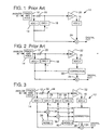
- a typical subranging ADC 10 is shown in Fig. 1. It includes a track and hold circuit 12, first and second ADCs 14, 16, a digital-to-analog converter (DAC) 18, a load 20, an amplifier 22, and a summer 24.
- DAC digital-to-analog converter
- an input analog signal is applied to the track and hold circuit 12.
- the output from this circuit tracks its input until a clock signal applied thereto causes the circuit to momentarily hold its output fixed.
- the first ADC 14 then converts this analog output signal into digital form, thereby providing a first approximation of the digitized value.
- ADC 14 The digital output from ADC 14 is converted back into analog current form by the DAC 18, causing an error, or residual voltage to be developed across the load 20. This residual voltage is amplified by the amplifier 22 and converted into digital form by the second ADC 16.
- the accuracy of ADC2 is less critical than ADC1 since it is only operating on the residual or "subrange" of the original signal. In the Fig. 1 system, the errors of ADC2 are only one 64th as significant as errors in ADC1.
- the summer 24 sums ADC1's first approximation of the input analog signal and ADC2's representation of the residual (appropriately adjusted for the gain of the amplifier) to provide a composite digital output signal.
- the advantage of the subranging approach is that the accuracy of the result is dependent only on the accuracy of the DAC and ADC2, not on the accuracy of ADC1.
- the size of the residual is still a function of ADC1 accuracy but the accuracy of the residual is not. This shifts the primary accuracy requirements to the DAC instead of the ADC, taking advantage of the inherently higher accuracy of DACs for a given sample rate.
- the principal limit on accuracy in subranging ADC 10 is the accuracy with which the DAC 18 converts the digital output of ADC1 14 back into analog form.
- the DAC 18 typically generates its output signals by controllably gating binarily weighted currents into a summation node in response to the bits of the digital input signal.
- the magnitudes of these component current sources are set by resistors internal to the DAC. High accuracies can be achieved by laser trimming each resistor in each DAC to achieve a desired measure of accuracy. However, such custom processing makes the DAC expensive and thus unsuitable for many applications. Mass produced DACs are much less expensive but can significantly compromise the accuracy of a subranging ADC.
- the correction circuit 26 includes a memory in which the error of each of the DAC's current sources is stored. By monitoring the digital signal applied to the DAC, the correction circuit 26 can determine the current sources that are active. calculate their cumulative error, and subtract this error from the final subranging ADC output signal.
- the present invention provides a technique wherein the errors of the component DAC current sources are determined automatically during the circuit's normal operation. This is achieved, in a preferred form of the invention, by continually introducing a random signal into the process, statistically examining the DAC output signal to discern error terms, and correlating the occurrences of these errors with the values of the random signal applied to the DAC so as to identify the current sources to which the error terms are due. The resulting output signal is compensated to remove the random signal and is further compensated to remove the DAC error terms discerned by this statistical analysis.
- the present invention in its most generalised form, is as specified in method claim 1 and system claim 21, hereinafter.
- Fig. 1 is a schematic block diagram of a prior art subranging analog to digital converter circuit.
- Fig. 2 is a schematic block diagram of a prior art subranging ADC that includes compensation to remove known DAC errors.
- Fig. 3 is a schematic block diagram of a subranging ADC that includes statistical autocalibration according to one embodiment of the present invention.
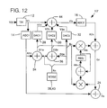
- Fig. 4 is a schematic block diagram of a correction circuit used in the subranging ADC of Fig. 3.
- Fig. 5 illustrates an ideal process
- Fig. 6 illustrates an actual process that includes a non-ideal process parameter P.
- Fig. 7 is a schematic block diagram of a generalized embodiment of the present invention.
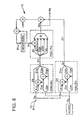
- Fig. 8 is the schematic block diagram of Fig. 7 annotated to detail the correspondence of its generalized functional blocks to their particular functions in the subranging ADC of Fig. 3.
- Fig. 9 illustrates an intermediate specialization of the generalized embodiment of Fig. 7 to a particular gain controlled amplifier embodiment.
- Fig. 10 illustrates another intermediate specialization of the generalized embodiment of Fig. 7 to a particular gain controlled amplifier embodiment.
- Fig. 11 is a schematic block diagram of an application of the generalized embodiment of Fig. 7 to a particular gain controlled amplifier application.
- the subranging ADC with which the present invention is illustated minimizes errors associated with non-ideal digital-to-analog conversion by two techniques. The first is to automatically quantify the error of each of the DAC current sources so the final digital output signal can be compensated for their cumulative error. The second is to randomize any remaining errors that may be due to imperfect quantification (and thus compensation) of the DAC current source errors.
- Fig. 3 shows a subranging ADC 10' employing the techniques of the present invention. Taking the randomization technique first, the single DAC of Figs. 1 and 2 is replaced by three DACs 28, 30, 32, two adders 34, 36, and two noise sources 38, 40. Since all three DAC current outputs are wired in parallel, the composite output is DAC1 + DAC2 + DAC3. (This summation is performed at a current node 44.) Assuming perfect DACs and tracing the DAC inputs back through the adders, the composite output can be seen to be -(ADC1 + NOISE1) + (NOISE1 + NOISE2) - (NOISE2), or -ADC1. This is the same effective DAC output as in the subranging ADC of Fig. 1 if the three DACs are perfectly accurate. The difference arises when the DAC errors are considered.
- DAC1 is driven directly by the output of ADC1, which in turn is directly determined by the sampled input voltage. In that case, any errors produced by the DAC are repeatably generated for any given input voltage. Consequently, the inaccuracies of the overall A/D converter system are repeatable and signal dependent. This means that even if multiple measurements are made of a certain signal, the errors cannot be averaged away since they are signal dependent and are repeated in all measurements.
- each DAC current source is driven by a bit stream which is determined by pure noise, or by noise combined with signal bits. If the noise signals are appropriately selected, only the most significant bit of DAC1 has any correlation with the input signal. This means that errors due to any of the other bits are injected in a manner completely independent of the input signal. The result is a noise-like error which can be averaged away using multiple A/D measurements. This characteristic is very beneficial in many applications. Even though this benefit alone is very important, a possibly more significant outcome is that this scheme provides a straight forward technique of determining the DAC current source errors for calibration.
- the autocalibration technique employed in the present invention relies on two statistical properties of the system's signals. The first is that the digital input bits applied to the three DACs are random (with the exception of the MSB of DAC1, as mentioned above). Consequently, it is equally probable during any given conversion cycle that any given input bit may be a "1" or a "0.” The second statistical property is that the final output signal from the A/D converter is uncorrelated to the values of the DAC input bits, since the input bits are randomized.
- Such a correlation may be due to a variety of factors.
- the dominant factor is the error by which the magnitude of the DAC current source differs from its ideal value. Assuming for a moment that all of the DAC current sources except one are ideal, and that this one current source is slightly larger than it should be, it may be recognized that the system's long term average output signal when that current source is energized will be slightly larger than the long term average output signal when that current source is idle. This is due to the slight additional current associated with this current source (but none of the others) that is added to the final output signal each time this current source is energized but is not added when it is idle. By examining the behavior of the output signal over the long term and correlating its behavior with the value of a given DAC input bit, the error of the associated DAC current source can be discerned.
- This correlation is effected by adding a greatly diminished version (i.e. by a factor of thousands or millions) of the corrected output signal to the error value stored in the correction circuit 26' if the corresponding DAC input bit is a "1", and subtracting the same value if the corresponding DAC input bit is a "0.” If the long term average of the output signal when the bit is a "1" is the same as the long term average when the bit is a "0," these additions and subtractions will cancel, leaving an error term of substantially zero.
- An analogy may be made to a statistical examination of the process of wagering on a coin toss. If a bettor wins $1.01 each time he calls the coin toss correctly but loses only $1.00 when he calls it incorrectly, he will not break even over the long term. Rather, he will come out ahead.
- a statistician who knows the bettor's winnings (or losses) over the long term can discern the difference between the two figures. If, after a million coin flips, the bettor has accumulated net winnings of $10,000, and the statistician knows the bettor loses $1.00 each time he calls the coin toss incorrectly, the statistician can compute that the bettor must win $1.01 each time he calls the toss correctly.
- the present invention relies on basically the same principle.
- the "known" in the present invention is the expected statistical behavior of the output signal over the long term as a function of each DAC input signal.
- the error of each of the DAC current sources can be determined and can be subtracted out using prior art techniques.
- the resulting A/D converter thus has several advantages. First is that the DAC errors are determined automatically during the system's normal operations and the resulting output signal is compensated to remove their effect. The second is that any remaining errors are randomized, permitting their substantial removal by time averaging techniques.
- ADC1 has N bits of resolution
- NOISE1 and NOISE2 should have N+1 and N bits of resolution respectively.
- all three of these digital signals are encoded as positive binary integers. If the converter is to be used for both positive and negative input signals, the conversion range of ADC1 must be offset such that a zero volt input produces a half scale output. This offset can then be accounted for in the interpretation of the final digital output. Since such an offset has no effect on the operation of the technique being described, it will be ignored in this discussion, and the converter will he described as handling positive inputs only.
- the N bits of NOISE2 are generated using N independent one-bit random binary sequence generators which are interpreted collectively as an N-bit binary coded random integer. Since all the bits are independent of each other, all states are equally likely and NOISE2 is uniformly distributed in the range from 0 to 2 N -1.
- N+1 bits of NOISE1 are similarly generated using N+1 independent one-bit random binary sequence generators. N of these are interpreted as an N-bit binary coded random integer. The remaining random bit (0 or 1) is then added to this random integer. The resulting range of NOISE1 is then 0 to 2 N , requiring N+1 bits for encoding.
- the required addition can be combined with adders shown in the block diagram rather than by using a separate adder inside the NOISE1 source. This is done by connecting the extra random bit to the carry-in of each of the two adders.
- the range of outputs is 0 to 2 (N + 1) -1 driving DAC1, 0 to 2 (N + 1) -1 driving DAC2 and 2 N -1 for DAC3.
- N + 1 the number of bits of resolution for DAC1, DAC2 and DAC3 are N+1, N+1 and N, respectively.
- the errors associated with each of the DAC current sources by the calibration technique are expressed in terms of their deviation from some reference.
- the choice of reference is not important as long as all the current source errors are consistently computed relative to that reference.
- the chosen reference becomes the "absolute" standard against which the sampled signal is measured.
- the reference is chosen to be the current source associated with the most significant bit of DAC1.
- This current reference is the absolute standard against which the signal current through the resistor 20 is measured. Since this current source is "perfect" by definition, it has no error and does not have to be calibrated. All the other N+1 bits used in the three DACs must be calibrated relative to the most significant bit of DAC1.
- the hardware 41 used in the correction circuit 26' to apply the calibration is shown in Fig. 4.
- each of the 3N+1 current sources to be calibrated has associated with it in correction circuit 26' an accumulator register 42 which holds the error of that particular current source. Since the desired correction accuracy is better than the original DAC resolution, the resolution of the accumulator must be finer than the resolution of the DAC.
- each accumulator 42 may be considered to store a fixed point two's complement binary number with M bits to the right of the point. The bit immediately to the left of the point is equivalent in significance to the LSB of ADC1, NOISE1 and NOISE2.
- the first step in the correction technique is to compute the correction needed for that sample. This is done by adders 43 that sum up the values in all the accumulator registers associated with the current sources which are on for that sample, i.e. all the DAC bits driven with a "1.” This correction value is then subtracted by a circuit 45 from the output of ADC2 to give a corrected residual output. This corrected residual must be computed to the full resolution of M bits to the right of the point.
- the second step of the calibration technique is to update the accumulator registers with new estimates of the current source errors. This is done by dividing the corrected residual by a smoothing factor of 2 k to achieve a feedback signal that tweaks the error constants stored in the accumulators. The choice of a power of two makes the division a simple right shift of the binary representation of the corrected residual. After the right shift, the feedback is rounded to M bits to the right of the point.
- Each of the 3N+1 accumulator registers is updated by adding or subtracting the feedback from the previous contents of the accumulator register. The choice of adding or subtracting depends on whether the DAC bit driving the current source associated with the register was a "1" or a "0" for the current sample. If the bit was a "1," an add is performed. If the bit was a "0,” a subtract is performed. The result yields the correct value of the current source errors in the accumulator registers.
- the smoothing factor 2 k there is a tradeoff between accuracy and the speed with which the technique can track changes to the DACs caused by aging, temperature, etc. Choosing very large smoothing factors reduces the variance of the current source error estimates held in the accumulator registers, giving more precise corrections. However, the time constant for tracking changes in a DAC is proportional to the sample period multiplied by the smoothing factor. Therefore, if the smoothing factor is set too large, the accumulator register may not contain a very accurate error estimate for a changing DAC error. Practical values for the smoothing factor range from 2 10 to 2 25 .
- the illustrated correction technique has significant advantages over currently used techniques in that an error model is generated and kept current without having to pause for a calibration cycle.
- the error model tracks relatively fast-moving changes in the DACs, allowing for greater precision.
- the DAC bits excluding the most significant bit of DAC1, are driven with noise-like signals which are signal independent, eliminating potential self heating errors which are signal dependent. Most remaining errors which are not removed are randomized across the entire frequency spectrum, allowing for further accuracy improvement using averaging.
- a random vector Z n is provided.
- a preprocessing operation C is performed on the input signal and random vector (X n ,Z n ) to yield an randomized version X n ' of the input signal.
- Fig. 8 is the generalized block diagram of Fig. 7 annotated to detail the correspondence of the generalized functional blocks with their particular functions in the specific A/D converter example.
- variable X n is a vector comprised of two components: the analog signal to be converted into digital form and a digital approximation of that analog signal. These components are labelled V n and A1 n , respectively in Fig. 8.
- P n is a set of adjustable parameters which models the conversion errors associated with the analog-to-digital conversion process (i.e. the DAC current source errors stored in the accumulators 42); and
- Z n is a two-component vector of digital noise integers Z1 n and Z2 n .
- the generalized function H yields a vector output of -1 or 1 values corresponding, respectively, to the (0,1) values of the individual bits of the binary representation of D1, D2 and D3, exclusive of the most significant bit of D1.
- the generalized function F is the sum of the analog signal V n , the output of three ideal D/A converters driven by -D1 n , D2 n , and -D3 n , and an error component for each D/A converter bit modeled by the dot product B n • P n.
- the resulting W n is an accurate digital representation of the difference between the analog component of the input V n and the digital estimate component A1 n .
- A1 n and W n an accurate final digital representation of V n is achieved.
- Fig. 11 shows a simple example - that of a gain controlled amplifier 50.
- P n adjustable parameter
- the input signal is again combined with a noise signal Z n , and this signal is passed through the non-ideal amplifier.
- the resulting output signal W n ' is processed by subtracting out the noise signal that has been correspondingly amplified.
- the remaining signal is then examined for correlation with the random input data by the same technique used above, namely by adding or subtracting (depending on the random signal) a weighted version of the output signal from an accumulator register that determines the amplifier gain.
- Figs. 9 - 10 show the series of substitutions by which the generalized diagram of Fig. 7 is specialized into the gain controlled amplifier application of Fig. 11.
- Fig. 10 shows that the function C here simply combines the input signal X n with the noise signal Z n .
- the track and hold block 12 takes a continuously changing voltage as an input and generates a sequence of samples voltages on the output. Both the input and output voltages can take on values with arbitrarily line resolution and are therefore represented as real numbers.
- the range of voltages on the input and output are assumed to be limited to the range of ⁇ RI 0 /2 where I 0 is the value of the MSB current source in DAC1, and R is an arbitrarily selected voltage to current scale factor to achieve the desired input range. Errors in the track and hold circuitry are not affected by the claimed methodology and are therefore not addressed in this discussion.
- the first ADC 14 converts the sampled voltage from the track-and-hold circuit 12 into a binary integer.
- the integer is constrained to be encoded with N bits, thus making this representation a rather coarse approximation of the samples input voltage.
- the errors associated with this coarse representation of the voltage are carried through the analysis as E 1 n. This allows verification that these errors are ultimately eliminated through the traditional use of a two-pass (subranging) converter approach. It also allows verification that these errors will not adversely effect the operation of the DAC error correction methodology which is the focus of this analysis.
- the purpose of the noise generator 38, 40 is to produce 2N+1 uncorrelated binary noise sequence which are used to generate random integers which can be combined with ADC1 outputs to drive the DACs.
- the noise At times in the following analysis it will be easier to consider the noise as individual random bit sequences denoted as x in . At other times it will be easier to consider them as binary representations of integers D 3 n and D 4 n .
- many of the Boolean operations which would normally occur in describing logic operations can be more conveniently represented in algebraic form if the states of x in are taken as ⁇ 1 rather than the traditional 0,1 states. This eases the calculation of correlation between bits.
- orthogonality criteria the technique used to generate the bit sequences meeting the orthogonality criteria will not be described here since a variety of approaches may be used. Fortunately, a strict adherence to the criteria is not absolutely necessary for the claimed methodology to work correctly. When considering techniques for generating the noise, the following analysis may be consulted to see where the criteria is applied and therefore which orthogonality conditions are really necessary.
- the integer sequences D 4 n and D 3 n can be defined as follows: where : D 4 n ⁇ Integers, 0 ⁇ D 4 n ⁇ 2 N where: D 3 n ⁇ Integers, 0 ⁇ D 3 n ⁇ 2 N -1
- the digital-to-analog converters 28, 30, 32 are assumed to be constructed as a set of independent binary weighted current sources with the outputs summed together in the analog adder (i.e. current node).
- the analog adder combines the DAC current outputs with the sampled input voltage to produce a residual voltage labeled v' n .
- the main thrust of this aspect of the calibration methodology is to eliminate the effects of inaccuracies in the binary weighting of the current sources in the DACs.
- a key assumption is that each binary bit entering the three DACs controls an individual current source which has a value c i independent of n and independent of the state of all other DAC bits. Although the c i values nominally are binary weighted within each DAC, this is not necessary.
- ADC2 Analog-to-Digital Converter 2
- the purpose of the second ADC 16 is to convert the residual voltage from the analog adder into digital form. Because of the finite number of bits in ADC2, the output becomes a quantized approximation of the real value of the residual. The error in this quantization will be denoted as E 2 n and is carried through the remainder of the analysis in order to show that it has no adverse effect on the correction algorithm. Normally, the residual voltage range is considerably smaller than the original input voltage. This allows ADC2 to operate over a smaller voltage range than ADC1, making
- the particular encoding scheme used for ADC2 is not important, although for this analysis it is assumed that the output is bipolar and centered around 0.
- a 2 n 2 N v' n RI 0 + E 2 n
- the purpose of the correction circuitry 26 is to correct each sample of the quantized residual by adding an appropriate correction for each bit which drove the DAC current sources when that sample was taken. By doing this, the DAC current errors can be removed. Even though the DAC model described above implies that a DAC current error only occurs with the drive bit equal to 1, the correction is applied for both the 1 and -1 states. Although this seems counter-intuitive, it actually yields better statistical properties for the errors inherent in the correction algorithm.
- the purpose of the correction hardware 41 is to update the correction vector, H n , based on the corrected residual and on the DAC drive bits for the current sample. This block maintains a running accumulation of the corrected residual times each DAC drive bit. If there is a correlation between there two sequences, the stored correction value will integrate to a new value until the correlation disappears. When the corrected residual no longer correlated to any of the DAC bits, the correction vector contains the appropriate values to offset the DAC current errors. The fact that this occurs and that the vector is independent of the input signal will be shown later.
- H n +1 H n + B n G n K
- the output adder 24 combines the coarse quantization results from ADC1 with the corrected residual to generate the composite digitized output from the converter.
- Y n A 1 n +G n
- the first part of this analysis calculates the deterministic portion of the output.
- the second part then examines the nature of the random noise which is inherent in the system.
- the output Y n can be computed in terms of v n . Since A 1 n is already defined in terms of v n , the challenging part of this derivation is to determine the corrected residual, G n , in terms of v n .
- the defining equation for G n can be expanded by substituting in the definitions for A 2 n and then v' n .Regrouping and factoring yields the following result.
- the factor (C+2 1-N H n ) becomes, in effect, the corrected current source weights for the DAC bits relative to the MSB of DAC1. These corrected bit weights will be designated as W n .
- W n would not change versus n and would be binary weighted values within each DAC.
- the characteristics of W n must be derived. This may be done by taking the defining equation for H n ,multiplying both sides by 2 1-N , adding C to both sides, and substituting in W n and G n .
- the recursive equation for W n can be solved by breaking W n down into a non-varying component, W, and a zero mean varying component,W' n .
- W n W+W' n
- the first term in the above equation for Y n is the ideal desired output.
- the second term is the error caused by the quantization and inaccuracies of ADC2.
- the third term, E 3 is a static inaccuracy due to the deviation of actual current source values, C, from the ideal current source values, W.
- the last term represents a zero-mean noise error which is injected by the correction methodology. The magnitude and spectral characteristics of this noise are computed in the following discussion.
- the spectral characteristics of the random noise portion of the output can be derived by forming the autocorrelation function of the noise, and then transforming to the frequency domain.
- the autocorrelation function, P m be defined as:
- G' n E 1 n + E 2 n + E 3
- the matrix inside the parenthese be represented by its expected value plus a zero-mean varying component , ⁇ n /K.
- the expected value has already been defined in terms of F such that
- G' n- i 2 The only remaining factor inside the expected value operation is G' n- i 2 . This may be made independent of i by recognizing that the expected value is independent of an offset in the index. Also, the order of summation can be reversed so that the summation over i is done first. For K >> 1 a very good approximation to the double summation is given in the following section on supporting derivations.
- P0 G 2 (3N+1) 2K where :
- the transient response is the summation of the independent geometric decay of 3N+1 orthogonal vectors corresponding to the rows of ⁇ . In order for the transient to decay ultimately to zero, it is required that
- bits of D 3 n are merely a renumbering of some of the noise bits directly from X n .
- b jn x j -N, n where: 2N+2 ⁇ j ⁇ 3N+1
- F is defined as the expected value of the correlations among the bits in the vector sequence B n .
- the entire correlation matrix F can be written as a partitioned matrix as: Where I represents an NxN identity matrix and where A and S are given below.
- F 0 is defined as the correlation between the MSB of DACl, b 0 n , and the rest of the DAC bits, B n .
- i identifies a particular entry in the vector.
- the expected values can be formulated using the formulas in the section labeled "B n versus X n ", and applying the orthogonality criteria to simplify the result.
- a few of the entries in the matrix are computed below to establish a pattern from which F 0 can be written.
- f 0N 1 2 N
- All elements f 0 i for i > N+1 are equal to zero due to the orthogonality criteria.
- the terms of the form ⁇ [a in q jn ] can be expanded into sums of the form ⁇ s ij . See the section on the derivation of F for this expansion. This allows F 0 to be expressed in matrix form using the definitions for A and S given in the previous section.
- the term -4 -N can be expressed as a function of A by noting the following: Therefore F 0 can be written as: Inversion of F to get F -1
- a convenient way to invert the correlation matrix is to assume a solution, multiply by F and force the result to be the identity matrix. This generates a set of simultaneous equations from which the elements of the inverse can be calculated. Since F is symmetric, the inverse must also be symmetric. Therefore let: The last two columns of the inverse are not computed since the inverse is only being used to multiply by F 0 , and the elements of F 0 multiplied by these columns are zero. Since there are seven unknowns to find in the inverse, seven independent equations must be generated from the identity above.
- the extremes of the range of x correspond to the extremes of A T S T SA.
- the maximum, value of A T S T SA labeled s max , occurs when all non-zero entries of S are the same sign and are their maximum magnitude (+1 or -1).
- the maximum value of x 2 is positive and less than 1, indicating that x is real, positive and less than 1.
Landscapes
- Engineering & Computer Science (AREA)
- Theoretical Computer Science (AREA)
- Analogue/Digital Conversion (AREA)
- Measurement Of Current Or Voltage (AREA)
Claims (24)
- Ein Verfahren zum Kompensieren von Fehlern, die in einem elektrischen Signal entstehen, das durch ein elektronisches System läuft, wobei ein elektrisches Dateneingangssignal zu dem System geliefert wird, und wobei das Eingangssignal von dem System verarbeitet wird, um ein elektrisches Datenausgangssignal zu liefern, wobei das Ausgangssignal ansprechend auf einen oder mehrere Prozeßparameter gestört ist, um zu bewirken, daß das Ausgangssignal von einem Idealwert abweicht, und um die Fehler zu bewirken,wobei das Verfahren folgende Schritte aufweist:Erfassen der Abweichungen in dem Ausgangssignal und Kompensieren des Systems ansprechend auf die erfaßten Abweichungen, um den Störungen entgegenzuwirken, und um das Ausgangssignal auf einen nahezu idealen Wert zurückzubringen, wobei das Erfassen und Kompensieren folgende Schritte aufweist: Erregen des Systems mit einem Zufallsrauschsignal, statistisches Analysieren des Verhaltens des Ausgangssignals durch Korrelieren des Ausgangssignals mit dem Rauschsignal, und Korrigieren der Fehler als Ergebnis einer solchen Korrelation;und wobei das elektrische Signal durch das System läuft, um einen abgetasteten Datenprozeß F zu erzeugen, aus dem die Abweichungen entfernt werden, um denselben näher zum Idealzustand zu bringen, wobei der Prozeß idealerweise folgendermaßen dargestellt ist:wobei der Prozeß tatsächlich einen oder mehrere Prozeßparameter umfaßt, die bewirken, daß der tatsächliche Prozeß vom Idealzustand abweicht, derart, daß der tatsächliche Prozeß folgendermaßen dargestellt ist:wobei der Prozeß derart ist, daßwobei das Verfahren folgende Schritte aufweist:Bereitstellen eines Zufallsvektors Zn;Durchführen einer Operation C auf (Xn,Zn), um ein Ausgangssignal Xn' zu ergeben;Durchführen der Operation F auf (Xn',Pn), um ein Ausgangssignal Wn' zu ergeben;Durchführen einer Operation H auf (Xn,Zn), um ein Vektorausgangssignal Zn' zu ergeben; undDurchführen einer Operation D auf (Wn',Zn'), um ein Ausgangssignal Wn zu ergeben;Berechnen des Parametervektors Pn+1 für den nächsten Abtastwert unter Verwendung folgender Formel:wobei:die Operationen C, H und D folgendermaßen ausgewählt sind, daß:
- Ein Verfahren gemäß Anspruch 1, bei dem folgendes gilt:
- Ein Verfahren gemäß Anspruch 1, bei dem Zn ein Skalierer ist, wobei folgendes gilt:
- Ein Verfahren gemäß Anspruch 3, bei dem der Prozeß F ein Verstärker ist, der eine variable Verstärkung Pn aufweist, wobei die erwünschte Verstärkung P ist, derart, daß folgender Zusammenhang gilt:
- Ein Verfahren gemäß Anspruch 1, bei demder Prozeß F ein Analog-zu-Digital-Signalumwandlungsprozeß ist;Xn ein Analogsignal ist, das in eine digitale Form umgewandelt werden soll;Yn das digitale Gegenstück von Xn ist;Pn ein Satz von einstellbaren Parametern ist, der die Umwandlungsfehler modelliert, die dem Analog-zu-Digital-Umwandlungsprozeß zugeordnet sind; undZn ein Vektor digitaler Rauschsignale ist.
- Ein Verfahren gemäß Anspruch 1, bei demXn eine Analogspannung Vn und drei digitale Zahlen A1n, A2n und A3n aufweist;wobei der ideale Prozeß folgendermaßen beschrieben ist:wobei der tatsächliche Prozeß folgendermaßen beschrieben ist:wobei der Zufallsvektor Zn aus zwei Zufallsdigitalzahlen besteht, und wobei Zn zwei Zufallsdigitalzahlen Z1n und Z2n umfaßt;wobei die Operation C ein Ausgangssignal Xn' erzeugt, das die analoge Spannung Vn und drei digitale Zahlen D1n, D2n und D3n aufweist, derart, daß:wobei die Operation D ein Ausgangssignal Wn erzeugt, derart, daß:wobei die Operation H ein Ausgangssignal Zn' erzeugt, das einen Vektor aller einzelnen Bits umfaßt, die verwendet werden, um die drei digitalen Zahlen D1n, D2n und D3n zu codieren.
- Ein Verfahren gemäß Anspruch 1, bei dem das elektronische System einen Umwandlungsfehler in einem Digital-zu-Analog-Wandler (DAW) kompensiert, der in einem Teilbereichs-Analog-zu-Digital-Wandler (ADW) verwendet wird, wobei das Verfahren das Anlegen eines Eingangssignals an den DAW und das Kompensieren eines Ausgangssignals, das durch den ADW erzeugt wird, unter Verwendung eines Fehlerterms, der dem DAW-Eingangssignal zugeordnet ist, aufweist;wobei das Verfahren folgende Schritte aufweist:Erregen des DAW mit einem Zufallssignal; undCharakterisieren des Fehlerterms basierend auf dem statistischen Verhalten des ADW-Ausgangssignals.
- Ein Verfahren gemäß Anspruch 7, bei dem das Zufallssignal eine Kombination einer digitalisierten Annäherung eines analogen Eingangssignals und eines Rauschsignals ist.
- Ein Verfahren gemäß Anspruch 8, das ferner folgenden Schritt aufweist:Kompensieren des DAW-Ausgangssignals, um die Rauschsignalkomponente aus demselben zu entfernen.
- Ein Verfahren gemäß Anspruch 9, bei demdem DAW eine Mehrzahl von Fehlertermen zugeordnet sind, wobei einer für jedes einer Mehrzahl von DAW-Eingangsbits vorgesehen ist;und wobei der Schritt des Charakterisierens folgende Schritte aufweist:Dekrementieren des Fehlerterms, der einem der Eingangsbits zugeordnet ist, um eine gewichtete Version des ADW-Ausgangssignals, wenn eine "0" an das Eingangsbit angelegt wird; undInkrementieren des Fehlerterms, der einem der Eingangsbits zugeordnet ist, um eine gewichtete Version des ADW-Ausgangssignals, wenn eine "1" an das Eingangsbit angelegt wird.
- Ein Verfahren gemäß Anspruch 10, das ferner folgenden Schritt aufweist:Gewichten des ADW-Ausgangssignals durch Bitverschieben.
- Ein Verfahren gemäß Anspruch 1, bei dem das elektronische System ein erwünschtes digitales Eingangssignal in ein analoges Signal, das demselben entspricht, umwandelt, wobei das Verfahren das Erregen eines Digital-zu-Analog-Wandlers und das Kompensieren eines resultierenden Ausgangssignals unter Verwendung eines Fehlerterms, der der Erregung zugeordnet ist, umfaßt; wobei das Verfahren folgenden Schritt aufweist:Abschätzen des Fehlerterms, während das erwünschte digitale Eingangssignal in ein analoges Signal umgewandelt wird, das demselben entspricht, und nicht bei einem reservierten Kalibrationszyklus.
- Ein Verfahren gemäß Anspruch 1, bei dem das elektronische System Fehler von Signalquellen in einem Digital-zu-Analog-Wandler (DAW) quantifiziert, wobei ein Referenzsignal, mit dem die Signalquellen verglichen werden, durch folgende Schritte erzeugt wird:Aufnehmen des DAW in das elektronische System;Erregen des DAW mit einem Zufallssignal; undstatistisches Analysieren des Verhaltens eines Signals, das von dem System erzeugt wird.
- Ein Verfahren gemäß Anspruch 1, bei dem das elektronische System einen Teilbereichs-Analog-zu-Digital-Wandler (ADW) aufweist, wobei das Verfahren folgende Schritte umfaßt:Erzeugen einer digitalen Annäherung eines analogen Eingangssignals;Umwandeln der digitalen Annäherung in ein analoges Zwischensignal, das derselben näherungsweise entspricht;Erzeugen eines analogen Teilbereichssignals durch Bestimmen einer Differenz zwischen dem analogen Eingangssignal und dem analogen Zwischensignal;Erzeugen einer digitalen Annäherung des Teilbereichssignals; undKombinieren der digitalen Annäherungen, um ein schließliches Ausgangssignal zu erhalten;und wobei die Schritte des Digital/Analog-Wandelns folgende Schritte aufweisen:Kombinieren der digitalen Annäherung des analogen Eingangssignals mit zumindest einem digitalen Rauschsignal, um ein kombiniertes digitales Signal zu ergeben;Umwandeln des kombinierten digitalen Signals in ein erstes analoges Zwischensignal, das demselben näherungsweise entspricht, unter Verwendung eines Digital-zu-Analog-Wandlers (DAW);Verarbeiten des ersten analogen Zwischensignals, um die Rauschkomponente von demselben zu entfernen; undfür zumindest ein Bit des DAW:Korrelieren des schließlichen Ausgangssignals mit einem Digitalwert, der durch das kombinierte digitale Signal an das Bit angelegt wird, um jede Abweichung von einem idealen DAW-Verhalten festzustellen.
- Ein Verfahren gemäß Anspruch 14, bei dem der Schritt des Korrelierens folgende Schritte aufweist:Gewichten eines Signals, das dem schließlichen Ausgangssignal entspricht, mit einem Faktor A, wenn das digitale Signal, das an das Bit angelegt wird, eine "0" ist;Gewichten eines Signals, das dem schließlichen Ausgangssignal entspricht, mit einem Faktor B, wenn das digitale Signal, das an das Bit angelegt wird, eine "1" ist;Bestimmen eines Langzeitmittels des gewichteten schließlichen Ausgangssignals; undFeststellen einer Abweichung zwischen dem Langzeitmittel und einem Referenzlangzeitmittel, das entstehen würde, wenn der DAW keinen Umwandlungsfehler hätte, wobei die Abweichung ein DAW-Umwandlungsfehler ist.
- Ein Verfahren gemäß Anspruch 15, bei dem das Referenzlangzeitmittel gleich (XA + YB) * Z ist, wobeiX die Wahrscheinlichkeit ist, daß das digitale Signal, das an das Bit angelegt wird, eine "0" ist;Y die Wahrscheinlichkeit ist, daß das digitale Signal, das an das Bit angelegt wird, eine "1" ist; undZ der erwartete Wert des schließlichen Ausgangssignals ist.
- Ein Verfahren gemäß Anspruch 15, das ferner das Kompensieren des schließlichen Signals umfaßt, um den Fehler zu entfernen, der durch den Schritt des Feststellens bestimmt wurde.
- Ein Verfahren gemäß Anspruch 15, das das Feststellen eines DAW-Umwandlungsfehlers für jedes einer Mehrzahl von DAW-Bits umfaßt.
- Ein Verfahren gemäß Anspruch 15, bei dem der Schritt des Feststellens folgende Schritte aufweist:Halten eines Speichers, in dem ein Wert gespeichert ist, der dem Umwandlungsfehler näherungsweise entspricht;Teilen des Signals, das dem schließlichen Ausgangssignal entspricht, durch eine große Zahl, um die Bedeutsamkeit desselben zu verringern;Addieren eines Werts, der dem verringerten Signal entspricht, zu dem in dem Speicher gespeicherten Wert, wenn das digitale Signal, das an das Bit angelegt wird, eine "0" ist; undSubtrahieren eines Werts, der dem verringerten Signal entspricht, von dem Wert, der in dem Speicher gespeichert ist, wenn das digitale Signal, das an das Bit angelegt wird, eine "1" ist.
- Ein Verfahren gemäß Anspruch 19, bei dem der Schritt des Teilens ein Bitverschieben des schließlichen Ausgangssignals umfaßt.
- Ein elektronisches System, bei dem Fehler, die in einem elektrischen Signal entstehen, das durch das System läuft, kompensiert werden, das eine Einrichtung zum Liefern eines elektrischen Dateneingangssignals zu dem System und eine Einrichtung zum Verarbeiten des Eingangssignals, um ein elektrisches Datenausgangssignal zu schaffen, aufweist, wobei das Ausgangssignal ansprechend auf einen oder mehrere Prozeßparameter gestört ist, um zu bewirken, daß das Ausgangssignal von einem Idealwert abweicht, und um die Fehler zu bewirken,wobei das System folgende Merkmale aufweist:eine Einrichtung zum Erfassen der Abweichungen in dem Ausgangssignal und zum Kompensieren des Systems ansprechend auf die erfaßten Abweichungen, um den Störungen entgegenzuwirken, und um das Ausgangssignal auf einen nahezu idealen Wert zurückzubringen, wobei die Einrichtung zum Erfassen und Kompensieren eine Einrichtung zum Erregen des Systems mit einem Zufallsrauschsignal, eine Einrichtung zum statistischen Analysieren des Verhaltens des Ausgangssignals durch Korrelieren des Ausgangssignals mit dem Rauschsignal, und eine Einrichtung zum Korrigieren der Fehler als Ergebnis einer solchen Korrelation aufweist;und wobei das elektrische Signal durch das System läuft, um einen abgetasteten Datenprozeß F zu erzeugen, aus dem die Abweichungen entfernt werden, um denselben idealer zu machen, wobei der Prozeß idealerweise folgendermaßen dargestellt ist:wobei Xn ein Eingangssignal ist, und Yn ein Skaliererausgangssignal ist, das demselben entspricht;wobei der Prozeß tatsächlich einen oder mehrere Prozeßparameter umfaßt, die bewirken, daß der tatsächliche Prozeß vom Idealzustand abweicht, derart, daß der tatsächliche Prozeß folgendermaßen dargestellt ist:wobei Xn das Eingangssignal ist, Pn ein Vektor ist, der die Parameter für den entsprechenden Abtastwert darstellt, und Yn' das Ausgangssignal des tatsächlichen Prozesses ist, das (Xn,Pn) entspricht;wobei der Prozeß derart ist, daßwobei P ein fester Vektor ist, der ideale Prozeßparameter darstellt;und wobei das elektronische System zusätzlich folgende Merkmale aufweist:eine Einrichtung zum Bereitstellen eines Zufallsvektors Zn;eine Einrichtung zum Durchführen einer Operation C auf (Xn,Zn), um ein Ausgangssignal Xn' zu ergeben;eine Einrichtung zum Durchführen der Operation F auf (Xn',Pn), um ein Ausgangssignal Wn' zu ergeben;eine Einrichtung zum Durchführen einer Operation H auf (Xn,Zn), um ein Vektorausgangssignal Zn' zu ergeben; undeine Einrichtung zum Durchführen einer Operation D auf (Wn',Zn'), um ein Ausgangssignal Wn zu ergeben;eine Einrichtung zum Berechnen des Parametervektors Pn+1 für den nächsten Abtastwert unter Verwendung folgender Formel:wobei K eine Glättungskonstante ist;wobeidie Operationen C, H und D folgendermaßen ausgewählt sind, daßunddas Vorzeichen jedes Elements des erwarteten Werts von [WnZn'] zu dem Vorzeichen des entsprechenden Elements des erwarteten Werts von [Pn-P] gleich ist.
- Ein System gemäß Anspruch 21, das einen Teilbereichs-Analog-zu-Digital-Wandler (10) aufweist, der folgende Merkmale umfaßt:einen ersten und einen zweiten Analog-zu-Digital-Wandler (ADW) (14, 16);einen Digital-zu-Analog-Wandler (DAW) (18);wobei jeder der Wandler einen Eingang und einen Ausgang hat;eine analoge Subtraktionsschaltung (20) mit einem ersten und einem zweiten Eingang und einem Differenzausgang;einen analogen Signaleingang, der mit dem ersten Eingang der Subtraktionsschaltung verbunden ist;wobei der Eingang des ersten ADW (14) mit dem analogen Signaleingang verbunden ist, und wobei der Ausgang des ersten ADW (14) mit dem Eingang des DAW (18) verbunden ist;wobei der Ausgang des DAW (18) mit dem zweiten Eingang der Subtraktionsschaltung (20) verbunden ist;wobei der Eingang des zweiten ADW (16) mit dem Differenzausgang der Subtraktionsschaltung verbunden ist; undeine Einrichtung (24) zum Kombinieren der Ausgänge des ersten und des zweiten ADW, um ein digitales Ausgangssignal zu liefern;und wobei der DAW (18) folgende Merkmale aufweist:einen ersten, einen zweiten und einen dritten DAW (28, 30, 32), von denen jeder einen Eingang und einen Ausgang hat;eine erste und eine zweite digitale Rauschquelle (38, 40), von denen jede einen Ausgang hat;einen ersten und einen zweiten Addierer (34, 36), von denen jeder zwei Eingänge und einen Ausgang hat; undeine Korrekturschaltung (26') mit einer Mehrzahl von Eingängen und einem Ausgang;wobei der erste Eingang des ersten Addierers (34) mit dem Ausgang der ersten Rauschquelle (38) gekoppelt ist, und wobei der zweite Eingang des ersten Addierers (34) mit dem Ausgang des ersten ADW (14) gekoppelt ist, wobei der Ausgang des Addierers mit dem Eingang des ersten DAW (28) gekoppelt ist, um die negierte Summe des Ausgangssignals der ersten Rauschquelle und des Ausgangssignals des ersten ADW an denselben anzulegen;wobei der erste Eingang des zweiten Addierers (36) mit dem Ausgang der ersten Rauschquelle (38) gekoppelt ist, und wobei der zweite Eingang des zweiten Addierers (36) mit dem Ausgang der zweiten Rauschquelle (40) gekoppelt ist, wobei der Ausgang des Addierers mit dem Eingang des zweiten DAW (30) gekoppelt ist, um die Summe der Ausgangssignale der ersten und der zweiten Rauschquelle zu demselben zu liefern;wobei der Eingang des dritten DAW (32) mit dem Ausgang der zweiten Rauschquelle (40) gekoppelt ist, um ein negiertes Rauschausgangssignal von derselben zu empfangen;wobei die Ausgänge des ersten, des zweiten und des dritten DAW (28, 30, 32) mit dem zweiten Eingang der analogen Subtraktionsschaltung (20) gekoppelt sind;wobei der erste Eingang der Korrekturschaltung (26') mit dem Ausgang des zweiten ADW (16) gekoppelt ist, wobei ein zweiter Eingang der Korrekturschaltung (26') mit dem Ausgang des ersten Addierers (34) gekoppelt ist, wobei ein dritter Eingang der Korrekturschaltung (26') mit dem Ausgang des zweiten Addierers (36) gekoppelt ist, und wobei ein vierter Eingang der Korrekturschaltung (26') mit dem Ausgang der zweiten Rauschquelle (40) gekoppelt ist, wobei die Schaltung eine Einrichtung (41) zum Kompensieren des digitalen Ausgangssignals bezüglich Umwandlungsfehlern in dem ersten, dem zweiten und dem dritten DAW umfaßt.
- Ein System gemäß Anspruch 23, das ferner folgende Merkmale aufweist:eine Speichereinrichtung (42) zum Speichern eines Umwandlungsfehlers, der jedem einer Mehrzahl von Eingangsbits des ersten, des zweiten und des dritten DAWs zugeordnet ist;eine Einrichtung (43) zum Kombinieren der Umwandlungsfehler gemäß digitaler Muster, die an den ersten, den zweiten und den dritten DAW angelegt werden, um einen Nettoumwandlungsfehler zu bestimmen; undeine Einrichtung (45) zum Kompensieren des digitalen Ausgangssignals, um den Nettoumwandlungsfehler zu berücksichtigen.
- Ein System gemäß Anspruch 23, das ferner folgendes Merkmal aufweist:eine Einrichtung (41) zum Aktualisieren der gespeicherten Umwandlungsfehler gemäß dem Ausgangssignal von dem zweiten ADW.
Priority Applications (1)
| Application Number | Priority Date | Filing Date | Title |
|---|---|---|---|
| EP94201105A EP0616433A1 (de) | 1989-11-27 | 1990-11-23 | Auf die Statistik basiertes kontinuierliches Autokalibrierungsverfahren und -gerät |
Applications Claiming Priority (2)
| Application Number | Priority Date | Filing Date | Title |
|---|---|---|---|
| US07/442,379 US4996530A (en) | 1989-11-27 | 1989-11-27 | Statistically based continuous autocalibration method and apparatus |
| US442379 | 1989-11-27 |
Related Child Applications (2)
| Application Number | Title | Priority Date | Filing Date |
|---|---|---|---|
| EP94201105A Division EP0616433A1 (de) | 1989-11-27 | 1990-11-23 | Auf die Statistik basiertes kontinuierliches Autokalibrierungsverfahren und -gerät |
| EP94201105.7 Division-Into | 1990-11-23 |
Publications (3)
| Publication Number | Publication Date |
|---|---|
| EP0430599A2 EP0430599A2 (de) | 1991-06-05 |
| EP0430599A3 EP0430599A3 (en) | 1993-04-14 |
| EP0430599B1 true EP0430599B1 (de) | 1998-10-21 |
Family
ID=23756589
Family Applications (2)
| Application Number | Title | Priority Date | Filing Date |
|---|---|---|---|
| EP90312766A Expired - Lifetime EP0430599B1 (de) | 1989-11-27 | 1990-11-23 | Auf statistischen Prinzipien basiertes kontinuierliches Autokalibrierungsverfahren und -gerät |
| EP94201105A Withdrawn EP0616433A1 (de) | 1989-11-27 | 1990-11-23 | Auf die Statistik basiertes kontinuierliches Autokalibrierungsverfahren und -gerät |
Family Applications After (1)
| Application Number | Title | Priority Date | Filing Date |
|---|---|---|---|
| EP94201105A Withdrawn EP0616433A1 (de) | 1989-11-27 | 1990-11-23 | Auf die Statistik basiertes kontinuierliches Autokalibrierungsverfahren und -gerät |
Country Status (5)
| Country | Link |
|---|---|
| US (1) | US4996530A (de) |
| EP (2) | EP0430599B1 (de) |
| JP (1) | JP3173783B2 (de) |
| CA (1) | CA2029944C (de) |
| DE (1) | DE69032710T2 (de) |
Cited By (1)
| Publication number | Priority date | Publication date | Assignee | Title |
|---|---|---|---|---|
| DE102004049348A1 (de) * | 2004-10-08 | 2006-04-20 | Micronas Gmbh | Verfahren sowie Einrichtung zur Kompensation von Kennlinienfehlern eines Analog-Digital-Wandlers |
Families Citing this family (85)
| Publication number | Priority date | Publication date | Assignee | Title |
|---|---|---|---|---|
| DE69223212T2 (de) * | 1991-08-15 | 1998-05-14 | Texas Instruments Inc | Kalibrierung eines aus einer rekonfigurierbaren Reihe von Stufen bestehenden Systems |
| US5721788A (en) | 1992-07-31 | 1998-02-24 | Corbis Corporation | Method and system for digital image signatures |
| US5539667A (en) * | 1992-09-15 | 1996-07-23 | Gcc Technologies | Method and apparatus for improved digital film recorder |
| US5493298A (en) * | 1993-03-01 | 1996-02-20 | Hewlett-Packard Company | Dithered analog-to-digital converter |
| US5862260A (en) * | 1993-11-18 | 1999-01-19 | Digimarc Corporation | Methods for surveying dissemination of proprietary empirical data |
| US6580819B1 (en) | 1993-11-18 | 2003-06-17 | Digimarc Corporation | Methods of producing security documents having digitally encoded data and documents employing same |
| US5822436A (en) * | 1996-04-25 | 1998-10-13 | Digimarc Corporation | Photographic products and methods employing embedded information |
| US5748783A (en) * | 1995-05-08 | 1998-05-05 | Digimarc Corporation | Method and apparatus for robust information coding |
| ATE287176T1 (de) * | 1993-11-18 | 2005-01-15 | Digimarc Corp | Video mit versteckten in-band digitalen daten |
| US5768426A (en) | 1993-11-18 | 1998-06-16 | Digimarc Corporation | Graphics processing system employing embedded code signals |
| US5710834A (en) * | 1995-05-08 | 1998-01-20 | Digimarc Corporation | Method and apparatus responsive to a code signal conveyed through a graphic image |
| US6611607B1 (en) | 1993-11-18 | 2003-08-26 | Digimarc Corporation | Integrating digital watermarks in multimedia content |
| US6408082B1 (en) | 1996-04-25 | 2002-06-18 | Digimarc Corporation | Watermark detection using a fourier mellin transform |
| US6122403A (en) * | 1995-07-27 | 2000-09-19 | Digimarc Corporation | Computer system linked by using information in data objects |
| US5841978A (en) * | 1993-11-18 | 1998-11-24 | Digimarc Corporation | Network linking method using steganographically embedded data objects |
| US5636292C1 (en) * | 1995-05-08 | 2002-06-18 | Digimarc Corp | Steganography methods employing embedded calibration data |
| US5841886A (en) * | 1993-11-18 | 1998-11-24 | Digimarc Corporation | Security system for photographic identification |
| US6449377B1 (en) * | 1995-05-08 | 2002-09-10 | Digimarc Corporation | Methods and systems for watermark processing of line art images |
| USRE40919E1 (en) * | 1993-11-18 | 2009-09-22 | Digimarc Corporation | Methods for surveying dissemination of proprietary empirical data |
| US6516079B1 (en) | 2000-02-14 | 2003-02-04 | Digimarc Corporation | Digital watermark screening and detecting strategies |
| US5748763A (en) * | 1993-11-18 | 1998-05-05 | Digimarc Corporation | Image steganography system featuring perceptually adaptive and globally scalable signal embedding |
| US6424725B1 (en) | 1996-05-16 | 2002-07-23 | Digimarc Corporation | Determining transformations of media signals with embedded code signals |
| US5832119C1 (en) * | 1993-11-18 | 2002-03-05 | Digimarc Corp | Methods for controlling systems using control signals embedded in empirical data |
| US7171016B1 (en) | 1993-11-18 | 2007-01-30 | Digimarc Corporation | Method for monitoring internet dissemination of image, video and/or audio files |
| US7044395B1 (en) | 1993-11-18 | 2006-05-16 | Digimarc Corporation | Embedding and reading imperceptible codes on objects |
| US6614914B1 (en) | 1995-05-08 | 2003-09-02 | Digimarc Corporation | Watermark embedder and reader |
| US6983051B1 (en) | 1993-11-18 | 2006-01-03 | Digimarc Corporation | Methods for audio watermarking and decoding |
| US6522770B1 (en) | 1999-05-19 | 2003-02-18 | Digimarc Corporation | Management of documents and other objects using optical devices |
| US7039214B2 (en) * | 1999-11-05 | 2006-05-02 | Digimarc Corporation | Embedding watermark components during separate printing stages |
| US6968057B2 (en) * | 1994-03-17 | 2005-11-22 | Digimarc Corporation | Emulsion products and imagery employing steganography |
| US6869023B2 (en) | 2002-02-12 | 2005-03-22 | Digimarc Corporation | Linking documents through digital watermarking |
| AT356U1 (de) * | 1994-09-15 | 1995-08-25 | Siemens Ag Oesterreich | Analog-digital-wandlerschaltung |
| US6560349B1 (en) | 1994-10-21 | 2003-05-06 | Digimarc Corporation | Audio monitoring using steganographic information |
| US6728390B2 (en) | 1995-05-08 | 2004-04-27 | Digimarc Corporation | Methods and systems using multiple watermarks |
| US6760463B2 (en) | 1995-05-08 | 2004-07-06 | Digimarc Corporation | Watermarking methods and media |
| US7486799B2 (en) * | 1995-05-08 | 2009-02-03 | Digimarc Corporation | Methods for monitoring audio and images on the internet |
| US6721440B2 (en) | 1995-05-08 | 2004-04-13 | Digimarc Corporation | Low visibility watermarks using an out-of-phase color |
| US6829368B2 (en) | 2000-01-26 | 2004-12-07 | Digimarc Corporation | Establishing and interacting with on-line media collections using identifiers in media signals |
| US7006661B2 (en) | 1995-07-27 | 2006-02-28 | Digimarc Corp | Digital watermarking systems and methods |
| US6408331B1 (en) * | 1995-07-27 | 2002-06-18 | Digimarc Corporation | Computer linking methods using encoded graphics |
| US6577746B1 (en) | 1999-12-28 | 2003-06-10 | Digimarc Corporation | Watermark-based object linking and embedding |
| US6788800B1 (en) | 2000-07-25 | 2004-09-07 | Digimarc Corporation | Authenticating objects using embedded data |
| US6965682B1 (en) | 1999-05-19 | 2005-11-15 | Digimarc Corp | Data transmission by watermark proxy |
| US6411725B1 (en) | 1995-07-27 | 2002-06-25 | Digimarc Corporation | Watermark enabled video objects |
| US6381341B1 (en) | 1996-05-16 | 2002-04-30 | Digimarc Corporation | Watermark encoding method exploiting biases inherent in original signal |
| US5959562A (en) * | 1997-09-03 | 1999-09-28 | Analog Devices, Inc. | Sigma-delta modulator and method for operating such modulator |
| US5926123A (en) * | 1997-12-08 | 1999-07-20 | Raytheon Company | Self calibration circuitry and algorithm for multipass analog to digital converter interstage gain correction |
| US7054463B2 (en) | 1998-01-20 | 2006-05-30 | Digimarc Corporation | Data encoding using frail watermarks |
| US6456450B1 (en) | 1998-12-04 | 2002-09-24 | International Business Machines Corporation | Method and apparatus for reducing track misregistration due to digital-to-analog converter quantization noise |
| US6380874B1 (en) * | 1999-07-12 | 2002-04-30 | National Instruments Corporation | System and method for self-calibrating a multi-bit delta-sigma analog to digital converter using dynamic element matching |
| US6323791B1 (en) * | 1999-10-13 | 2001-11-27 | Analog Devices, Inc. | Control systems and methods for reducing residue signal offset in subranging analog-to-digital converters |
| US6625297B1 (en) * | 2000-02-10 | 2003-09-23 | Digimarc Corporation | Self-orienting watermarks |
| SE517536C2 (sv) | 2000-03-14 | 2002-06-18 | Ericsson Telefon Ab L M | Anordning samt metod för bakgrundskalibrering av A/D- omvandlare |
| US6496173B1 (en) * | 2000-03-29 | 2002-12-17 | Koninklijke Philips Electronics N.V. | RLCD transconductance sample and hold column buffer |
| US6466189B1 (en) * | 2000-03-29 | 2002-10-15 | Koninklijke Philips Electronics N.V. | Digitally controlled current integrator for reflective liquid crystal displays |
| US6804377B2 (en) | 2000-04-19 | 2004-10-12 | Digimarc Corporation | Detecting information hidden out-of-phase in color channels |
| US7027614B2 (en) | 2000-04-19 | 2006-04-11 | Digimarc Corporation | Hiding information to reduce or offset perceptible artifacts |
| US7171542B1 (en) * | 2000-06-19 | 2007-01-30 | Silicon Labs Cp, Inc. | Reconfigurable interface for coupling functional input/output blocks to limited number of i/o pins |
| US6404369B1 (en) * | 2000-09-29 | 2002-06-11 | Teradyne, Inc. | Digital to analog converter employing sigma-delta loop and feedback DAC model |
| US6901422B1 (en) | 2001-03-21 | 2005-05-31 | Apple Computer, Inc. | Matrix multiplication in a vector processing system |
| US6563444B2 (en) * | 2001-03-30 | 2003-05-13 | Iowa State University Research Foundation, Inc. | Apparatus for and method of performing a conversion operation |
| DE10133538B4 (de) * | 2001-07-11 | 2004-02-19 | Infineon Technologies Ag | Kalibriereinrichtung zur Kalibrierung von A/D-Wandlern mit beliebigem Bitgewicht |
| US6489913B1 (en) | 2001-09-24 | 2002-12-03 | Tektronix, Inc. | Sub-ranging analog-to-digital converter using a sigma delta converter |
| US6817530B2 (en) | 2001-12-18 | 2004-11-16 | Digimarc Id Systems | Multiple image security features for identification documents and methods of making same |
| ATE552120T1 (de) * | 2001-12-24 | 2012-04-15 | L 1 Secure Credentialing Inc | Verdeckte variableninformationen auf id- dokumenten und verfahren zu ihrer herstellung |
| US7793846B2 (en) * | 2001-12-24 | 2010-09-14 | L-1 Secure Credentialing, Inc. | Systems, compositions, and methods for full color laser engraving of ID documents |
| US7728048B2 (en) * | 2002-12-20 | 2010-06-01 | L-1 Secure Credentialing, Inc. | Increasing thermal conductivity of host polymer used with laser engraving methods and compositions |
| US7694887B2 (en) * | 2001-12-24 | 2010-04-13 | L-1 Secure Credentialing, Inc. | Optically variable personalized indicia for identification documents |
| US6781531B2 (en) | 2002-01-15 | 2004-08-24 | Raytheon Company | Statistically based cascaded analog-to-digital converter calibration technique |
| US7824029B2 (en) | 2002-05-10 | 2010-11-02 | L-1 Secure Credentialing, Inc. | Identification card printer-assembler for over the counter card issuing |
| US7804982B2 (en) | 2002-11-26 | 2010-09-28 | L-1 Secure Credentialing, Inc. | Systems and methods for managing and detecting fraud in image databases used with identification documents |
| DE10255354B3 (de) | 2002-11-27 | 2004-03-04 | Infineon Technologies Ag | A/D-Wandler mit minimiertem Umschaltfehler |
| US7712673B2 (en) | 2002-12-18 | 2010-05-11 | L-L Secure Credentialing, Inc. | Identification document with three dimensional image of bearer |
| DE10305972A1 (de) * | 2003-02-13 | 2004-09-02 | Micronas Gmbh | Kompensationsschaltungsanordnung und Kompensationsverfahren zum Kompensieren von nicht-linearen Verzerrungen eines AD-Wandlers |
| DE602004030434D1 (de) | 2003-04-16 | 2011-01-20 | L 1 Secure Credentialing Inc | Dreidimensionale datenspeicherung |
| US7744002B2 (en) * | 2004-03-11 | 2010-06-29 | L-1 Secure Credentialing, Inc. | Tamper evident adhesive and identification document including same |
| US7221299B2 (en) * | 2004-06-12 | 2007-05-22 | Nordic Semiconductor Asa | Method and apparatus for an ADC circuit with wider input signal swing |
| US20060022854A1 (en) * | 2004-07-29 | 2006-02-02 | Johnny Bjornsen | Method and apparatus for operating correlator of an ADC circuit |
| US7015851B1 (en) * | 2004-10-26 | 2006-03-21 | Agilent Technologies, Inc. | Linearizing ADCs using single-bit dither |
| US7277033B1 (en) * | 2006-02-13 | 2007-10-02 | Honeywell International, Inc. | System and method for subtracting dither reference during analog-to-digital conversion |
| TW201128961A (en) * | 2010-02-04 | 2011-08-16 | Nat Univ Chung Cheng | Current-mode digital-to-analog converter with prospective correction mechanism |
| US9735797B2 (en) | 2015-12-15 | 2017-08-15 | Analog Devices, Inc. | Digital measurement of DAC timing mismatch error |
| US9716509B2 (en) | 2015-12-15 | 2017-07-25 | Analog Devices, Inc. | Digital measurement of DAC switching mismatch error |
| US10630304B1 (en) * | 2019-04-01 | 2020-04-21 | Nxp B.V. | Sub-ranging analog-to-digital converter |
| US20240213992A1 (en) * | 2022-12-22 | 2024-06-27 | Intel Corporation | Digital-to-analog converter and method for amplitude and skew error correction in the digital-to-analog converter |
Family Cites Families (16)
| Publication number | Priority date | Publication date | Assignee | Title |
|---|---|---|---|---|
| US4328552A (en) * | 1980-01-17 | 1982-05-04 | Stovall Robert E | Statistical calibration system |
| US4342983A (en) * | 1980-08-11 | 1982-08-03 | Westinghouse Electric Corp. | Dynamically calibrated successive ranging A/D conversion system and D/A converter for use therein |
| US4775852A (en) * | 1980-11-07 | 1988-10-04 | Schlumberger Systems & Services, Inc. | Apparatus for compensating digital to analog converter errors |
| US4465995A (en) * | 1980-11-07 | 1984-08-14 | Fairchild Camera And Instrument Corp. | Method and apparatus for analyzing an analog-to-digital converter with a nonideal digital-to-analog converter |
| US4583075A (en) * | 1980-11-07 | 1986-04-15 | Fairchild Camera And Instrument Corporation | Method and apparatus for analyzing an analog-to-digital converter with a nonideal digital-to-analog converter |
| US4740776A (en) * | 1980-11-07 | 1988-04-26 | Fairchild Camera & Instrument Corporation | Apparatus for compensating digital to analog converter errors |
| US4550309A (en) * | 1984-02-16 | 1985-10-29 | Hewlett Packard Company | Analog to digital converter |
| US4673917A (en) * | 1984-07-18 | 1987-06-16 | Fairchild Semiconductor Corporation | Method and apparatus for minimizing digital-to-analog converter correction trims |
| US4612533A (en) * | 1985-06-12 | 1986-09-16 | The United States Of America As Represented By The Secretary Of The Air Force | Harmonic distortion reduction technique for data acquistion |
| US4903023A (en) * | 1985-11-06 | 1990-02-20 | Westinghouse Electric Corp. | Subranging analog-to-digital converter with digital error correction |
| JPS62204617A (ja) * | 1986-03-05 | 1987-09-09 | Seiko Instr & Electronics Ltd | 高分解能a/dコンバ−タ |
| NL8600815A (nl) * | 1986-03-28 | 1987-10-16 | At & T & Philips Telecomm | Inrichting voor het kompenseren van niet-lineaire vervorming in een te digitaliseren ingangssignaal en een echokompensatiestelsel voorzien van een dergelijke inrichting. |
| GB8705923D0 (en) * | 1987-03-12 | 1987-04-15 | Gen Electric Co Plc | Analogue to digital converter |
| JPS63224521A (ja) * | 1987-03-13 | 1988-09-19 | Nippon Precision Saakitsutsu Kk | D/a変換装置 |
| US4903024A (en) * | 1987-10-23 | 1990-02-20 | Westinghouse Electric Corp. | A/D converter system with error correction and calibration apparatus and method |
| US4897650A (en) * | 1988-04-05 | 1990-01-30 | General Electric Company | Self-characterizing analog-to-digital converter |
-
1989
- 1989-11-27 US US07/442,379 patent/US4996530A/en not_active Expired - Lifetime
-
1990
- 1990-11-14 CA CA002029944A patent/CA2029944C/en not_active Expired - Fee Related
- 1990-11-23 DE DE69032710T patent/DE69032710T2/de not_active Expired - Fee Related
- 1990-11-23 EP EP90312766A patent/EP0430599B1/de not_active Expired - Lifetime
- 1990-11-23 EP EP94201105A patent/EP0616433A1/de not_active Withdrawn
- 1990-11-27 JP JP32875290A patent/JP3173783B2/ja not_active Expired - Fee Related
Cited By (1)
| Publication number | Priority date | Publication date | Assignee | Title |
|---|---|---|---|---|
| DE102004049348A1 (de) * | 2004-10-08 | 2006-04-20 | Micronas Gmbh | Verfahren sowie Einrichtung zur Kompensation von Kennlinienfehlern eines Analog-Digital-Wandlers |
Also Published As
| Publication number | Publication date |
|---|---|
| CA2029944C (en) | 2000-11-07 |
| JP3173783B2 (ja) | 2001-06-04 |
| EP0616433A1 (de) | 1994-09-21 |
| JPH03181227A (ja) | 1991-08-07 |
| DE69032710D1 (de) | 1998-11-26 |
| US4996530A (en) | 1991-02-26 |
| EP0430599A3 (en) | 1993-04-14 |
| EP0430599A2 (de) | 1991-06-05 |
| CA2029944A1 (en) | 1991-05-28 |
| DE69032710T2 (de) | 1999-03-11 |
Similar Documents
| Publication | Publication Date | Title |
|---|---|---|
| EP0430599B1 (de) | Auf statistischen Prinzipien basiertes kontinuierliches Autokalibrierungsverfahren und -gerät | |
| Siragusa et al. | Gain error correction technique for pipelined analogue-to-digital converters | |
| Salib et al. | A high-precision time skew estimation and correction technique for time-interleaved ADCs | |
| Galton | Digital cancellation of D/A converter noise in pipelined A/D converters | |
| US6667706B2 (en) | Analog to digital converter | |
| US6734818B2 (en) | Digital cancellation of D/A converter noise in pipelined A/D converters | |
| US20200356620A1 (en) | Bit-Ordered Binary-Weighted Multiplier-Accumulator | |
| US6456223B1 (en) | Pipelined analog to digital converter using digital mismatch noise cancellation | |
| Galton et al. | A rigorous error analysis of D/A conversion with dynamic element matching | |
| EP1339169B1 (de) | Verfahren und Schaltungsanordnung zur Kalibrierung eines Analog-Digital Wandlers | |
| KR20200062209A (ko) | 혼성 신호 컴퓨팅 시스템 및 방법 | |
| US4903026A (en) | Architecture for high sampling rate, high resolution analog-to-digital converter system | |
| US12503982B2 (en) | System and methods for mixed-signal computing | |
| CN113114247A (zh) | 基于比较时间探测器的流水线adc级间增益校准方法 | |
| CN100479328C (zh) | 用于数字到模拟以及模拟到数字转换器的数字补偿的系统和方法 | |
| CN110034759B (zh) | 前馈式全数字tiadc系统的采样时间误差校准模块及其方法 | |
| KR940004326B1 (ko) | 캐리 프리딕션을 이용한 고성능 가산기 | |
| Arpaia et al. | Analytical a priori approach to phase-plane modeling of SAR A/D converters | |
| EP1049002A2 (de) | Verfahren und Gerät zum effizienten Berechnen eines annähernden Quadrats einer Festkommazahl | |
| Peng et al. | A low-power low-cost on-chip digital background calibration for pipelined ADCs | |
| Zhao et al. | Real-time Digital Background Calibration Technology for Integral Non-linearity of Analog to Digital Converters | |
| Divi et al. | Scalable blind calibration of timing skew in high-resolution time-interleaved ADCs | |
| US10587279B1 (en) | Digital to analog converter device and calibration method | |
| WO2005041417A2 (en) | Digital input signals constructor providing analog representation thereof | |
| Brenna et al. | A tool for the assisted design of charge redistribution SAR ADCs |
Legal Events
| Date | Code | Title | Description |
|---|---|---|---|
| PUAI | Public reference made under article 153(3) epc to a published international application that has entered the european phase |
Free format text: ORIGINAL CODE: 0009012 |
|
| AK | Designated contracting states |
Kind code of ref document: A2 Designated state(s): DE FR GB IT |
|
| PUAL | Search report despatched |
Free format text: ORIGINAL CODE: 0009013 |
|
| AK | Designated contracting states |
Kind code of ref document: A3 Designated state(s): DE FR GB IT |
|
| 17P | Request for examination filed |
Effective date: 19930921 |
|
| 17Q | First examination report despatched |
Effective date: 19950911 |
|
| GRAG | Despatch of communication of intention to grant |
Free format text: ORIGINAL CODE: EPIDOS AGRA |
|
| GRAG | Despatch of communication of intention to grant |
Free format text: ORIGINAL CODE: EPIDOS AGRA |
|
| GRAH | Despatch of communication of intention to grant a patent |
Free format text: ORIGINAL CODE: EPIDOS IGRA |
|
| GRAH | Despatch of communication of intention to grant a patent |
Free format text: ORIGINAL CODE: EPIDOS IGRA |
|
| GRAA | (expected) grant |
Free format text: ORIGINAL CODE: 0009210 |
|
| AK | Designated contracting states |
Kind code of ref document: B1 Designated state(s): DE FR GB IT |
|
| DX | Miscellaneous (deleted) | ||
| REF | Corresponds to: |
Ref document number: 69032710 Country of ref document: DE Date of ref document: 19981126 |
|
| ET | Fr: translation filed | ||
| PLBE | No opposition filed within time limit |
Free format text: ORIGINAL CODE: 0009261 |
|
| STAA | Information on the status of an ep patent application or granted ep patent |
Free format text: STATUS: NO OPPOSITION FILED WITHIN TIME LIMIT |
|
| 26N | No opposition filed | ||
| REG | Reference to a national code |
Ref country code: GB Ref legal event code: 732E |
|
| REG | Reference to a national code |
Ref country code: GB Ref legal event code: 732E |
|
| REG | Reference to a national code |
Ref country code: FR Ref legal event code: TP |
|
| REG | Reference to a national code |
Ref country code: FR Ref legal event code: TP |
|
| REG | Reference to a national code |
Ref country code: GB Ref legal event code: IF02 |
|
| PG25 | Lapsed in a contracting state [announced via postgrant information from national office to epo] |
Ref country code: IT Free format text: LAPSE BECAUSE OF NON-PAYMENT OF DUE FEES Effective date: 20051123 |
|
| PGFP | Annual fee paid to national office [announced via postgrant information from national office to epo] |
Ref country code: GB Payment date: 20071128 Year of fee payment: 18 Ref country code: FR Payment date: 20071119 Year of fee payment: 18 |
|
| PGFP | Annual fee paid to national office [announced via postgrant information from national office to epo] |
Ref country code: DE Payment date: 20081120 Year of fee payment: 19 |
|
| GBPC | Gb: european patent ceased through non-payment of renewal fee |
Effective date: 20081123 |
|
| REG | Reference to a national code |
Ref country code: FR Ref legal event code: ST Effective date: 20090731 |
|
| PG25 | Lapsed in a contracting state [announced via postgrant information from national office to epo] |
Ref country code: GB Free format text: LAPSE BECAUSE OF NON-PAYMENT OF DUE FEES Effective date: 20081123 |
|
| PG25 | Lapsed in a contracting state [announced via postgrant information from national office to epo] |
Ref country code: DE Free format text: LAPSE BECAUSE OF NON-PAYMENT OF DUE FEES Effective date: 20100601 |
|
| PG25 | Lapsed in a contracting state [announced via postgrant information from national office to epo] |
Ref country code: FR Free format text: LAPSE BECAUSE OF NON-PAYMENT OF DUE FEES Effective date: 20081130 |