EP0430487B1 - Matrixadressierbare Anzeigevorrichtungen - Google Patents
Matrixadressierbare Anzeigevorrichtungen Download PDFInfo
- Publication number
- EP0430487B1 EP0430487B1 EP90312404A EP90312404A EP0430487B1 EP 0430487 B1 EP0430487 B1 EP 0430487B1 EP 90312404 A EP90312404 A EP 90312404A EP 90312404 A EP90312404 A EP 90312404A EP 0430487 B1 EP0430487 B1 EP 0430487B1
- Authority
- EP
- European Patent Office
- Prior art keywords
- regions
- gate
- plate
- electrode
- polysilicon
- Prior art date
- Legal status (The legal status is an assumption and is not a legal conclusion. Google has not performed a legal analysis and makes no representation as to the accuracy of the status listed.)
- Expired - Lifetime
Links
- 239000011159 matrix material Substances 0.000 title description 8
- 210000004027 cell Anatomy 0.000 claims description 33
- 229910021420 polycrystalline silicon Inorganic materials 0.000 claims description 29
- 229920005591 polysilicon Polymers 0.000 claims description 27
- 238000000034 method Methods 0.000 claims description 13
- 239000004973 liquid crystal related substance Substances 0.000 claims description 6
- 210000002858 crystal cell Anatomy 0.000 claims description 5
- 239000000463 material Substances 0.000 claims description 5
- 238000010586 diagram Methods 0.000 description 6
- 239000000758 substrate Substances 0.000 description 6
- VYPSYNLAJGMNEJ-UHFFFAOYSA-N Silicium dioxide Chemical compound O=[Si]=O VYPSYNLAJGMNEJ-UHFFFAOYSA-N 0.000 description 5
- 239000003990 capacitor Substances 0.000 description 4
- 238000005468 ion implantation Methods 0.000 description 4
- 238000004519 manufacturing process Methods 0.000 description 4
- 239000004020 conductor Substances 0.000 description 3
- 235000012239 silicon dioxide Nutrition 0.000 description 3
- 239000010409 thin film Substances 0.000 description 3
- 229910052782 aluminium Inorganic materials 0.000 description 2
- XAGFODPZIPBFFR-UHFFFAOYSA-N aluminium Chemical compound [Al] XAGFODPZIPBFFR-UHFFFAOYSA-N 0.000 description 2
- 239000004411 aluminium Substances 0.000 description 2
- 230000000694 effects Effects 0.000 description 2
- 239000011521 glass Substances 0.000 description 2
- AMGQUBHHOARCQH-UHFFFAOYSA-N indium;oxotin Chemical compound [In].[Sn]=O AMGQUBHHOARCQH-UHFFFAOYSA-N 0.000 description 2
- 239000000377 silicon dioxide Substances 0.000 description 2
- 229910021417 amorphous silicon Inorganic materials 0.000 description 1
- 230000015572 biosynthetic process Effects 0.000 description 1
- 230000005669 field effect Effects 0.000 description 1
- 239000011810 insulating material Substances 0.000 description 1
- 230000000873 masking effect Effects 0.000 description 1
- 238000000206 photolithography Methods 0.000 description 1
- 239000010453 quartz Substances 0.000 description 1
- 239000004065 semiconductor Substances 0.000 description 1
- 230000001360 synchronised effect Effects 0.000 description 1
- 238000002834 transmittance Methods 0.000 description 1
Images


Classifications
-
- G—PHYSICS
- G02—OPTICS
- G02F—OPTICAL DEVICES OR ARRANGEMENTS FOR THE CONTROL OF LIGHT BY MODIFICATION OF THE OPTICAL PROPERTIES OF THE MEDIA OF THE ELEMENTS INVOLVED THEREIN; NON-LINEAR OPTICS; FREQUENCY-CHANGING OF LIGHT; OPTICAL LOGIC ELEMENTS; OPTICAL ANALOGUE/DIGITAL CONVERTERS
- G02F1/00—Devices or arrangements for the control of the intensity, colour, phase, polarisation or direction of light arriving from an independent light source, e.g. switching, gating or modulating; Non-linear optics
- G02F1/01—Devices or arrangements for the control of the intensity, colour, phase, polarisation or direction of light arriving from an independent light source, e.g. switching, gating or modulating; Non-linear optics for the control of the intensity, phase, polarisation or colour
- G02F1/13—Devices or arrangements for the control of the intensity, colour, phase, polarisation or direction of light arriving from an independent light source, e.g. switching, gating or modulating; Non-linear optics for the control of the intensity, phase, polarisation or colour based on liquid crystals, e.g. single liquid crystal display cells
- G02F1/133—Constructional arrangements; Operation of liquid crystal cells; Circuit arrangements
- G02F1/136—Liquid crystal cells structurally associated with a semi-conducting layer or substrate, e.g. cells forming part of an integrated circuit
- G02F1/1362—Active matrix addressed cells
- G02F1/1368—Active matrix addressed cells in which the switching element is a three-electrode device
-
- G—PHYSICS
- G02—OPTICS
- G02F—OPTICAL DEVICES OR ARRANGEMENTS FOR THE CONTROL OF LIGHT BY MODIFICATION OF THE OPTICAL PROPERTIES OF THE MEDIA OF THE ELEMENTS INVOLVED THEREIN; NON-LINEAR OPTICS; FREQUENCY-CHANGING OF LIGHT; OPTICAL LOGIC ELEMENTS; OPTICAL ANALOGUE/DIGITAL CONVERTERS
- G02F1/00—Devices or arrangements for the control of the intensity, colour, phase, polarisation or direction of light arriving from an independent light source, e.g. switching, gating or modulating; Non-linear optics
- G02F1/01—Devices or arrangements for the control of the intensity, colour, phase, polarisation or direction of light arriving from an independent light source, e.g. switching, gating or modulating; Non-linear optics for the control of the intensity, phase, polarisation or colour
- G02F1/13—Devices or arrangements for the control of the intensity, colour, phase, polarisation or direction of light arriving from an independent light source, e.g. switching, gating or modulating; Non-linear optics for the control of the intensity, phase, polarisation or colour based on liquid crystals, e.g. single liquid crystal display cells
- G02F1/133—Constructional arrangements; Operation of liquid crystal cells; Circuit arrangements
- G02F1/136—Liquid crystal cells structurally associated with a semi-conducting layer or substrate, e.g. cells forming part of an integrated circuit
- G02F1/1362—Active matrix addressed cells
- G02F1/136259—Repairing; Defects
- G02F1/136268—Switch defects
-
- G—PHYSICS
- G02—OPTICS
- G02F—OPTICAL DEVICES OR ARRANGEMENTS FOR THE CONTROL OF LIGHT BY MODIFICATION OF THE OPTICAL PROPERTIES OF THE MEDIA OF THE ELEMENTS INVOLVED THEREIN; NON-LINEAR OPTICS; FREQUENCY-CHANGING OF LIGHT; OPTICAL LOGIC ELEMENTS; OPTICAL ANALOGUE/DIGITAL CONVERTERS
- G02F2201/00—Constructional arrangements not provided for in groups G02F1/00 - G02F7/00
- G02F2201/12—Constructional arrangements not provided for in groups G02F1/00 - G02F7/00 electrode
- G02F2201/122—Constructional arrangements not provided for in groups G02F1/00 - G02F7/00 electrode having a particular pattern
-
- G—PHYSICS
- G02—OPTICS
- G02F—OPTICAL DEVICES OR ARRANGEMENTS FOR THE CONTROL OF LIGHT BY MODIFICATION OF THE OPTICAL PROPERTIES OF THE MEDIA OF THE ELEMENTS INVOLVED THEREIN; NON-LINEAR OPTICS; FREQUENCY-CHANGING OF LIGHT; OPTICAL LOGIC ELEMENTS; OPTICAL ANALOGUE/DIGITAL CONVERTERS
- G02F2202/00—Materials and properties
- G02F2202/10—Materials and properties semiconductor
- G02F2202/104—Materials and properties semiconductor poly-Si
Definitions
- FIG. 3 shows the circuit diagram of Figure 2 further modified to illustrate the actual configuration resulting from a practical embodiment of the invention.
- a single transistor channel 41 is common to the transistors T11 and T12, and a single transistor channel 43 is common to the transistors T21 and T22.
- Gate electrodes 45 and 47 of the transistors T11 and T12 are interconnected, and are connected to the line 25 via a common gate resistor 49.
- gate electrodes 51 and 53 of the transistors T21 and T22 are interconnected, and are connected to the line 23 via a common gate resistor 55.
- a common source connection 57 on the channel 41 is connected to the line 23 at a point 59, and a common source connection 61 on the channel 43 is connected to the line 27 at a point 61.
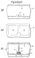
- Areas 87,89 ( Figure 4(e)) of transparent conductive material such as indium tin oxide, are deposited over the insulating layer and connected via the holes 77 and 81 to the drain electrodes. These areas form the electrodes 3 of the cells C11 and C12.
- Figure 4 (f) shows the completed region of the substrate 63, which is then finally annealed at 425°C.
- the figure shows the same component references as on Figure 3.
Landscapes
- Physics & Mathematics (AREA)
- Nonlinear Science (AREA)
- Engineering & Computer Science (AREA)
- Microelectronics & Electronic Packaging (AREA)
- Mathematical Physics (AREA)
- Chemical & Material Sciences (AREA)
- Crystallography & Structural Chemistry (AREA)
- General Physics & Mathematics (AREA)
- Optics & Photonics (AREA)
- Liquid Crystal (AREA)
- Devices For Indicating Variable Information By Combining Individual Elements (AREA)
- Thin Film Transistor (AREA)
Claims (6)
- Verfahren zur Herstellung einer Anzeigevorrichtung mit einer Gruppe schaltbarer Zellen (C11, C12, C21, C22), die zwischen einer ersten Platte und einer zu dieser im wesentlichen parallelen zweiten Platte angeordnet sind, wobei jede Zelle eine erste Elektrode (3) auf der ersten Platte und eine zweite Elektrode (5) auf der zweiten Platte aufweist, jeder Transistor einer Vielzahl von Transistoren (T11, T12, T21, T22), die auf der ersten Platte angeordnet sind, zwei Hauptelektroden und eine Gatt-Elektrode aufweist und die Hauptelektroden jedes Transistors zwischen jeweils einer Zellenelektrode auf der ersten Platte und einer ersten Adressenleitung (23, 27) angeschlossen sind und die Gatt-Elektrode jedes Transistors mit einer zweiten Adressenleitung (25, 23) verbunden ist; wobei das Verfahren umfaßt: die Ausbildung einer Vielzahl von PolysiliciumKanalbereichen (41, 43) für die Transistoren auf der ersten Platte; das Isolieren der Kanalbereiche; die Ausbildung von Polysilicium-Gatt-Bereichen (71, 73) für die Transistoren über den Kanalbereichen zusammen mit einer Vielzahl langgestreckter Polysilicium-Bereiche (69) mit einem vorbestimmten Verhältnis von Breite zu Länge, die mit den Gatt-Bereichen verbunden sind; das gleichzeitige Dotieren der Polysilicium-Gatt-Bereiche, der Kanal-Bereiche, wo sie nicht durch die Gatt-Bereiche dotiert sind, und der langgestreckten Polysilicium-Bereiche; wobei das vorbestimmte Verhältnis von Breite zu Länge so gewählt ist, daß die langgestreckten Bereiche, wenn sie dotiert sind, ohmsche Widerstandselemente (49) bilden, deren Widerstandswert hinreichend groß ist, um einen Adressenleitungskurzschluß zu verhindern; die zweite Adressenleitung so gebildet wird, daß sie mit denjenigen Enden der Polysilicium-Widerstandselemente verbunden sind, die den Gatt-Bereichen abgekehrt sind, und die ersten Elektroden so gebildet werden, daß sie mit den Kanal-Bereichen verbunden sind.
- Verfahren nach Anspruch 1, bei dem jeder Bereich der Vielzahl von Kanal-Bereichen (41, 43) zwei der Transistoren (T11-T22) bildet.
- Verfahren nach Anspruch 2, bei dem den beiden Transistoren ein einziges ohmsches Widerstandselement (49) gemeinsam ist.
- Verfahren nach einem der vorstehenden Ansprüche, bei dem jede Zelle (C11-C22) eine Flüssigkristallzelle ist.
- Anzeigevorrichtung mit einer Gruppe schaltbarer Zellen (C11, C12, C21, C22), die zwischen einer ersten und einer hierzu im wesentlichen parallelen zweiten Platte angeordnet sind, wobei jede Zelle eine erste Elektrode (3) auf der ersten Platte und eine zweite Elektrode auf der zweiten Platte aufweist, jeder Transistor einer Vielzahl von Transistoren (T11, T12, T21, T22), die auf der ersten Platte angeordnet sind, zwei Hauptelektroden und eine Gatt-Elektrode aufweist und die Hauptelektroden jedes Transistors jeweils zwischen einer Zellenelektrode auf der ersten Platte und einer ersten Adressenleitung (23, 27) angeschlossen sind und die Gatt-Elektrode jedes Transistors mit einer zweiten Adressenleitung (25, 23) über ein ohmsches Widerstandselement (49) verbunden ist, wobei das Widerstandselement einen langgestreckten Bereich aus dotiertem Polysiliciummaterial aufweist; ein Kanal-Bereich und ein Gatt-Bereich jedes Transistors dotiertes Polysiliciummaterial aufweisen, der langgestreckte Bereich und die Kanal- und Gatt-Bereiche gleichzeitig dotiert worden sind; und der langgestreckte Bereich ein vorbestimmtes Verhältnis von Breite zu Länge aufweist, das so gewählt ist, daß der Widerstandswert des Widerstandselements, das durch den dotierten langgestreckten Bereich gebildet wird, hinreichend groß ist, um einen Adressenleitungskurzschluß zu verhindern.
- Anzeigevorrichtung nach Anspruch 5, bei der jede Zelle (C11-C22) eine Flüssigkristallzelle ist.
Applications Claiming Priority (2)
| Application Number | Priority Date | Filing Date | Title |
|---|---|---|---|
| GB8926960 | 1989-11-29 | ||
| GB8926960A GB2238644B (en) | 1989-11-29 | 1989-11-29 | Matrix addressable displays |
Publications (3)
| Publication Number | Publication Date |
|---|---|
| EP0430487A2 EP0430487A2 (de) | 1991-06-05 |
| EP0430487A3 EP0430487A3 (en) | 1992-04-29 |
| EP0430487B1 true EP0430487B1 (de) | 1995-05-17 |
Family
ID=10667110
Family Applications (1)
| Application Number | Title | Priority Date | Filing Date |
|---|---|---|---|
| EP90312404A Expired - Lifetime EP0430487B1 (de) | 1989-11-29 | 1990-11-14 | Matrixadressierbare Anzeigevorrichtungen |
Country Status (5)
| Country | Link |
|---|---|
| US (1) | US5278086A (de) |
| EP (1) | EP0430487B1 (de) |
| JP (1) | JPH03198380A (de) |
| DE (1) | DE69019475T2 (de) |
| GB (1) | GB2238644B (de) |
Families Citing this family (2)
| Publication number | Priority date | Publication date | Assignee | Title |
|---|---|---|---|---|
| GB2265486A (en) * | 1992-03-11 | 1993-09-29 | Marconi Gec Ltd | Display device fabrication |
| TW526462B (en) * | 2000-04-06 | 2003-04-01 | Chi Mei Optoelectronics Corp | Method for reducing flicker and uneven brightness of LCD screen |
Citations (1)
| Publication number | Priority date | Publication date | Assignee | Title |
|---|---|---|---|---|
| FR2593631A1 (fr) * | 1986-01-27 | 1987-07-31 | Maurice Francois | Ecran d'affichage a matrice active a resistance de grille et procedes de fabrication de cet ecran |
Family Cites Families (11)
| Publication number | Priority date | Publication date | Assignee | Title |
|---|---|---|---|---|
| US4406997A (en) * | 1981-09-30 | 1983-09-27 | International Business Machines Corporation | Method and means for minimizing the effect of short circuits in flat panel displays |
| JPS59195871A (ja) * | 1983-04-20 | 1984-11-07 | Mitsubishi Electric Corp | Mos電界効果トランジスタの製造方法 |
| FR2554286B1 (fr) * | 1983-11-02 | 1985-12-27 | Comp Generale Electricite | Dispositif de protection contre des courts-circuits dans une matrice de composants electroniques |
| US4963503A (en) * | 1984-04-09 | 1990-10-16 | Hosiden Electronics Co., Ltd. | Method of manufacturing liquid crystal display device |
| US4775861A (en) * | 1984-11-02 | 1988-10-04 | Nec Corporation | Driving circuit of a liquid crystal display panel which equivalently reduces picture defects |
| US4678282A (en) * | 1985-02-19 | 1987-07-07 | Ovonic Imaging Systems, Inc. | Active display matrix addressable without crossed lines on any one substrate and method of using the same |
| GB8508656D0 (en) * | 1985-04-03 | 1985-05-09 | Gen Electric Co Plc | Liquid crystal displays |
| JPS6265375A (ja) * | 1985-09-17 | 1987-03-24 | Nippon Telegr & Teleph Corp <Ntt> | 半導体薄膜トランジスタ及びそれを用いた表示装置 |
| FR2593632B1 (fr) * | 1986-01-27 | 1988-03-18 | Maurice Francois | Ecran d'affichage a matrice active et procedes de realisation de cet ecran |
| JPS63101829A (ja) * | 1986-10-17 | 1988-05-06 | Nec Corp | アクテイブ・マトリツクス液晶表示装置およびその製造方法 |
| JPH0786615B2 (ja) * | 1987-10-06 | 1995-09-20 | 日本電気株式会社 | 液晶ライトバルブ |
-
1989
- 1989-11-29 GB GB8926960A patent/GB2238644B/en not_active Expired - Fee Related
-
1990
- 1990-11-14 EP EP90312404A patent/EP0430487B1/de not_active Expired - Lifetime
- 1990-11-14 DE DE69019475T patent/DE69019475T2/de not_active Expired - Fee Related
- 1990-11-27 JP JP2325130A patent/JPH03198380A/ja active Pending
- 1990-11-27 US US07/618,651 patent/US5278086A/en not_active Expired - Fee Related
Patent Citations (1)
| Publication number | Priority date | Publication date | Assignee | Title |
|---|---|---|---|---|
| FR2593631A1 (fr) * | 1986-01-27 | 1987-07-31 | Maurice Francois | Ecran d'affichage a matrice active a resistance de grille et procedes de fabrication de cet ecran |
Also Published As
| Publication number | Publication date |
|---|---|
| GB2238644B (en) | 1994-02-02 |
| GB8926960D0 (en) | 1990-01-17 |
| US5278086A (en) | 1994-01-11 |
| JPH03198380A (ja) | 1991-08-29 |
| DE69019475D1 (de) | 1995-06-22 |
| GB2238644A (en) | 1991-06-05 |
| EP0430487A2 (de) | 1991-06-05 |
| EP0430487A3 (en) | 1992-04-29 |
| DE69019475T2 (de) | 1995-10-05 |
Similar Documents
| Publication | Publication Date | Title |
|---|---|---|
| US4589733A (en) | Displays and subassemblies having improved pixel electrodes | |
| US5062690A (en) | Liquid crystal display with redundant FETS and redundant crossovers connected by laser-fusible links | |
| US5159477A (en) | Active matrix display device having additional capacitors connected to switching elements and additional capacitor common line | |
| CA1262954A (en) | Displays and subassemblies having optimized capacitance | |
| US4024626A (en) | Method of making integrated transistor matrix for flat panel liquid crystal display | |
| EP0460747B1 (de) | Verfahren zur Herstellung von Matrixen von MIM-Anordnungen und solche Matrixen enthaltende Anzeigevorrichtungen | |
| US4728175A (en) | Liquid crystal display having pixels with auxiliary capacitance | |
| US4728172A (en) | Subassemblies for displays having pixels with two portions and capacitors | |
| EP0209113B1 (de) | Redundante Leiterstrukturen für dünnfilm-FET-angesteuerte Flüssigkristallanzeigevorrichtungen | |
| KR100260359B1 (ko) | 액정 표시 장치 및 그 제조방법 | |
| US4917467A (en) | Active matrix addressing arrangement for liquid crystal display | |
| EP0197703B1 (de) | Flüssigkristallanzeigen | |
| JPH01166020A (ja) | 多重レベル回路の製造方法および多重レベル回路 | |
| EP0379249B1 (de) | Anzeigevorrichtungen mit aktiver Matrix-Adressierung | |
| US5952675A (en) | Thin film transistor element array | |
| US5337172A (en) | Liquid crystal matrix control employing doped semiconductor pixel electrode surrounded by undoped channel region | |
| US5508765A (en) | Matrix-addressed type display device | |
| US5432625A (en) | Display screen having opaque conductive optical mask and TFT of semiconductive, insulating, and conductive layers on first transparent conductive film | |
| JPS61153692A (ja) | 光影響性デイスプレイで使用されるプログラム可能な半導体スイツチ及びその製法 | |
| EP0760966B1 (de) | Struktur für flüssigkristall-anzeigevorrichtungen mit grossem öffnungsverhältnis | |
| US5278086A (en) | Matrix addressable displays | |
| US5058995A (en) | Pixel electrode structure for liquid crystal display devices | |
| KR100219504B1 (ko) | 이중 게이트 구조를 갖는 박막 트랜지스터-액정 표시장치 및 그 제조방법 | |
| JPS58192090A (ja) | マトリツクスアレ− | |
| JP2687967B2 (ja) | 液晶表示装置 |
Legal Events
| Date | Code | Title | Description |
|---|---|---|---|
| PUAI | Public reference made under article 153(3) epc to a published international application that has entered the european phase |
Free format text: ORIGINAL CODE: 0009012 |
|
| AK | Designated contracting states |
Kind code of ref document: A2 Designated state(s): DE FR IT NL |
|
| PUAL | Search report despatched |
Free format text: ORIGINAL CODE: 0009013 |
|
| AK | Designated contracting states |
Kind code of ref document: A3 Designated state(s): DE FR IT NL |
|
| 17P | Request for examination filed |
Effective date: 19921028 |
|
| 17Q | First examination report despatched |
Effective date: 19940721 |
|
| GRAA | (expected) grant |
Free format text: ORIGINAL CODE: 0009210 |
|
| AK | Designated contracting states |
Kind code of ref document: B1 Designated state(s): DE FR IT NL |
|
| PG25 | Lapsed in a contracting state [announced via postgrant information from national office to epo] |
Ref country code: IT Free format text: LAPSE BECAUSE OF FAILURE TO SUBMIT A TRANSLATION OF THE DESCRIPTION OR TO PAY THE FEE WITHIN THE PRE;WARNING: LAPSES OF ITALIAN PATENTS WITH EFFECTIVE DATE BEFORE 2007 MAY HAVE OCCURRED AT ANY TIME BEFORE 2007. THE CORRECT EFFECTIVE DATE MAY BE DIFFERENT FROM THE ONE RECORDED.SCRIBED TIME-LIMIT Effective date: 19950517 |
|
| ET | Fr: translation filed | ||
| REF | Corresponds to: |
Ref document number: 69019475 Country of ref document: DE Date of ref document: 19950622 |
|
| PLBE | No opposition filed within time limit |
Free format text: ORIGINAL CODE: 0009261 |
|
| STAA | Information on the status of an ep patent application or granted ep patent |
Free format text: STATUS: NO OPPOSITION FILED WITHIN TIME LIMIT |
|
| 26N | No opposition filed | ||
| PG25 | Lapsed in a contracting state [announced via postgrant information from national office to epo] |
Ref country code: NL Effective date: 19960601 |
|
| PG25 | Lapsed in a contracting state [announced via postgrant information from national office to epo] |
Ref country code: FR Effective date: 19960731 |
|
| NLV4 | Nl: lapsed or anulled due to non-payment of the annual fee |
Effective date: 19960601 |
|
| PG25 | Lapsed in a contracting state [announced via postgrant information from national office to epo] |
Ref country code: DE Effective date: 19960801 |
|
| REG | Reference to a national code |
Ref country code: FR Ref legal event code: ST |