EP0425776A1 - Package for a solid-state imaging device - Google Patents
Package for a solid-state imaging device Download PDFInfo
- Publication number
- EP0425776A1 EP0425776A1 EP90114971A EP90114971A EP0425776A1 EP 0425776 A1 EP0425776 A1 EP 0425776A1 EP 90114971 A EP90114971 A EP 90114971A EP 90114971 A EP90114971 A EP 90114971A EP 0425776 A1 EP0425776 A1 EP 0425776A1
- Authority
- EP
- European Patent Office
- Prior art keywords
- plate
- semiconductor device
- light
- chip
- lower plate
- Prior art date
- Legal status (The legal status is an assumption and is not a legal conclusion. Google has not performed a legal analysis and makes no representation as to the accuracy of the status listed.)
- Granted
Links
Images





Classifications
-
- H—ELECTRICITY
- H10—SEMICONDUCTOR DEVICES; ELECTRIC SOLID-STATE DEVICES NOT OTHERWISE PROVIDED FOR
- H10F—INORGANIC SEMICONDUCTOR DEVICES SENSITIVE TO INFRARED RADIATION, LIGHT, ELECTROMAGNETIC RADIATION OF SHORTER WAVELENGTH OR CORPUSCULAR RADIATION
- H10F77/00—Constructional details of devices covered by this subclass
- H10F77/50—Encapsulations or containers
-
- H—ELECTRICITY
- H10—SEMICONDUCTOR DEVICES; ELECTRIC SOLID-STATE DEVICES NOT OTHERWISE PROVIDED FOR
- H10F—INORGANIC SEMICONDUCTOR DEVICES SENSITIVE TO INFRARED RADIATION, LIGHT, ELECTROMAGNETIC RADIATION OF SHORTER WAVELENGTH OR CORPUSCULAR RADIATION
- H10F77/00—Constructional details of devices covered by this subclass
- H10F77/30—Coatings
- H10F77/306—Coatings for devices having potential barriers
- H10F77/331—Coatings for devices having potential barriers for filtering or shielding light, e.g. multicolour filters for photodetectors
- H10F77/334—Coatings for devices having potential barriers for filtering or shielding light, e.g. multicolour filters for photodetectors for shielding light, e.g. light blocking layers or cold shields for infrared detectors
-
- H—ELECTRICITY
- H10—SEMICONDUCTOR DEVICES; ELECTRIC SOLID-STATE DEVICES NOT OTHERWISE PROVIDED FOR
- H10W—GENERIC PACKAGES, INTERCONNECTIONS, CONNECTORS OR OTHER CONSTRUCTIONAL DETAILS OF DEVICES COVERED BY CLASS H10
- H10W72/00—Interconnections or connectors in packages
- H10W72/50—Bond wires
- H10W72/551—Materials of bond wires
- H10W72/552—Materials of bond wires comprising metals or metalloids, e.g. silver
- H10W72/5524—Materials of bond wires comprising metals or metalloids, e.g. silver comprising aluminium [Al]
Definitions
- the present invention relates to a semiconductor device and more particularly to a package for a solid-state imaging device.
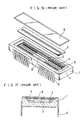
- Figure 16 is a partially exploded perspective view showing a conventional semiconductor device and figure 17 is a sectional view showing the same.
- reference numeral 1 designates a multi-layer ceramic plate formed of alumina (Al2O3)
- reference numeral 2 designates an image sensor chip diebonded to a bottom surface of the multiple-layer ceramic plate
- reference numeral 3 designates a wire made of metal which electrically connects a pad 4 on the chip to an inner lead 5 on the multiple-layer ceramic plate
- reference numeral 6 designates an outer lead electrically connected to said inner lead 5 by a multiple-layer wiring (not shown) in the multiple-layer ceramic plate
- reference numeral 7 designates a light shielding plate preventing light from radiating to a part other than the image area 8
- reference numeral 9 designates a glass lid bonded to the multi-layer ceramic plate 1 by a resin.
- Incident light from an upper surface of the device passes through the glass lid 9. Then, only light passing through an opening of the light shielding plate 7 reaches the image area 8 on the image sensor chip 2. Then, an image signal is converted to an electrical signal by photo-electric effect. This electric signal is output to the outer lead 6 through the pad 4, the wire 3, the inner lead 5 and the multiple-layer wiring (not shown) of the multi-layer ceramic plate 1 made of alumina.
- Figure 18 is a graph showing the relation between an amount of curvature and a distance from the chip center. As shown in figure 18, when the chip has an overall length of 85 mm, curvature of 200 ⁇ m is generated. Therefore, in the conventional semiconductor device, incident light from an optical system does not focus on the image area, so that the semiconductor device does not normally operate and internal stress in the chip is high at a room temperature and then reliability against the heat cycle and the like is low.
- the present invention was made in order to solve these problems and it is an object of the present invention to provide a semiconductor device in which curvature of a chip surface is little, incident light from an optical system focuses on an image area, a chip can normally operate, internal stress of the chip is low and reliability against a heat cycle and the like is sufficiently high.
- a semiconductor device in accordance with the present invention comprises a lower plate formed of a material which hardly transmits light with high insulation resistance and high mechanical intensity and has coefficient of linear expansion almost the same as that of the semiconductor chip, a middle plate comprising a single-layer or a multiple-layer wiring board and an upper plate formed of a material which hardly transmits light with high insulation resistance and high mechanical intensity and has coefficient of linear expansion almost the same as that of the lower plate and having a window for incident light, in which they are bonded to each other and an upper part of the upper plate is sealed by a lid formed of glass or a synthetic resin.
- a lower plate and an upper plate of a semiconductor device are formed of a material which has high insulation resistance and high mechanical intensity and coefficient of linear expansion almost the same as that of a semiconductor chip, and hardly transmits light, when they are bonded with putting a middle plate serving as a wiring board therebetween at a high temperature and then cooled to a room temperature (25 °C), one of shrinkage force on both sides of the middle plate emulates the other, with the result, that curvature of the chip surface is reduced and internal stress of the chip can be lowered.
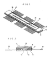
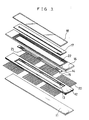
- FIG. 1 is a perspective view showing a semiconductor device in accordance with a first embodiment of the present invention and figures 2 and 3 are a sectional view and an exploded perspective view showing the same, respectively.
- reference numeral 11 designates a lower plate with a thickness of 1 mm which is formed of silicon carbide (SiC ; coefficient of linear expansion is 3.7 ⁇ 10 ⁇ 6 [°K ⁇ 1])
- reference numeral 12 designates a middle plate having an inner lead 13 and formed of alumina (Al2O3 ; coefficient of linear expansion is 6.8 ⁇ 10 ⁇ 6 [°K ⁇ 1]).
- the middle plate 12 comprising three laminated layers each having a thickness of 0.5 mm.
- Reference numeral 14 designates an image sensor chip with a thickness of 0.
- Reference numeral 16 is an upper plate with a thickness of 1.5 mm, formed of silicon carbide bonded on a middle plate 12.
- Reference numeral 17 designates a light shielding plate formed of stainless with a thickness of approximately 0.2 mm which is plated with delustering chrome and set in a frame-shaped trench on the upper plate 16.
- Reference numeral 18 designates a glass lid with a thickness of 1 mm which seals the frame part of the upper plate 16.
- Reference numeral 19 designates an aluminum wire with a diameter of 30 ⁇ m which connects the pad 15 on the image sensor chip 14 to the inner lead 13 on the middle plate 12 and reference numeral 20 designates an outer lead bonded to the middle plate 12.
- reference numeral 21 designates an image area formed on the image sensor chip and reference numeral 22 designates a rectangular opening for incident light provided at the upper plate 16.
- the middle plate 12 has a three layer structure and these three layers are baked together to be one plate.
- Each of the upper plate 16, the middle plate 12 and the lower plate 11 is mirror-ground on both surfaces and has a flatness of 20 - 50 ⁇ m over the whole surface.
- the glass lid 18 and the upper plate 16, the upper plate 16 and the middle plate 12, the middle plate 12 and the lower plate 11, and the image sensor chip 14 and the lower plate 11 are bonded by solder or an adhesive material such as resin, respectively, so that they are integrally formed.
- Mirror grinding is performed for preventing the plate from curving before bonding and for reducing an amount of the adhesive material used in bonding.
- Incident light from an upper surface of the device passes through the glass lid 18. Then, some light passes through an opening of the light shielding plate 17 and then reaches the image area 21 on the image sensor chip 14. Then, an image signal is converted to an electric signal. This electric signal is output to the outer lead 20 through the pad 15, the wire 19, the inner lead 13 and the multiple-layer wiring (not shown) of the middle plate 12 made of alumina.
- the lower plate 11 and the upper plate 16 are formed of silicon carbide which has a coefficient of linear expansion very close to that of silicon which constitutes the chip 14 and they are bonded at a high temperature with putting the middle plate serving as a wiring board therebetween and cooled to a room temperature (25 °C).
- One of shrinkage force on both sides of the middle plate caused by a temperature difference due to cooling operation emulates the other because the upper plate 16 and the lower plate 11 have the same coefficient of linear expansion, with the result that the curvature of the surface of the chip 14 is reduced.
- Figure 15 shows a result of simulation of the relation between an amount of curvature of the surface of the chip 14 and a distance from the center of the chip 14.
- the amount of curvature of the chip surface in a longitudinal direction is reduced to approximately 35 ⁇ m.
- the curvature of the chip is caused because the upper plate 16 has a window 22 for incident light and there is generated imbalance between the upper plate 16 and the lower plate 11.
- curvature of approximately 35 ⁇ m has almost no problem when light from an optical system focuses on the chip 14 and the device normally operates.
- the amount of curvature is small, internal stress of the chip is reduced and reliability against heat cycle is improved.
- the light shielding plate 17 is set in the trench on the upper plate 16 in this embodiment, this may be set in a trench formed on the middle plate 12.
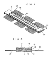
- Figures 4, 5 and 6 show a perspective view, a sectional view and an exploded perspective view showing a structure of a semiconductor device in accordance with a second embodiment of the present invention, respectively.
- the same references as in figure 1 designate the same parts.
- the chip 14 can be arranged in the vicinity of the light shielding plate 17 and light incident on a part other than the image area 21 on the chip 14 is prevented, so that stray light can be reduced. As a result, performance of the device can be further improved.
- FIG 7 is a sectional view showing a semiconductor device in accordance with a third embodiment of the present invention.
- the same references as in figure 5 designate the same parts.
- the glass lid 18 on the frame of the upper plate 16 is provided in contact with the light shielding plate 17 set on the top layer of the middle plate 12.
- weight of the device can be reduced and the device can be highly integrated, in addition to the effect in the second embodiment.
- the light shielding plate 17 may be set in a trench formed on a lower surface of the upper plate 16 apart from the glass lid 18 and it may be provided in the vicinity of the chip 14 as shown in figure 8 showing a fourth embodiment of the present invention.
- the glass lid 18 may be provided in contact with the light shielding plate 17 set in the bottom surface of the upper plate 16 as shown in figure 9 showing a fifth embodiment of the present invention. As a result, weight of the device is reduced and the device can be highly integrated.
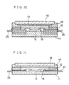
- the middle plate 12 In a case where it is necessary to increase an area of a brazing material at a root of the outer lead 20 bonded to the middle plate 12, the middle plate 12 should be thickly formed to have five layers and a die pad part of the lower plate 11 may be raised as shown in figure 10 showing a sixth embodiment of the present invention.
- the die pad part of the lower plate 11 is raised in order to easily perform wire bonding of the chip 14.
- the area for brazing the outer lead 20 is increased, tensile stress of the outer lead 20 is increased, with the result that reliability of the device is extremely improved.
- the light shielding plate may be dispensed with as shown in figure 11 showing a seventh embodiment of the present invention.
- the semiconductor device in accordance with this embodiment has very small internal stress and high reliability of heat cycle and the like as compared with those in accordance with the first to seventh embodiments. Especially, the device in accordance with this embodiment is effective when this is used for a space environment, such as an artificial satellite which requires high performance.
- silicon carbide is used as a material of the lower plate 11 and the upper plate 16 in the above embodiments
- a material which hardly transmits light with high insulation resistance and high mechanical intensity and has a coefficient of linear expansion close to that of material constituting the chip for example aluminum nitride (AlN; coefficient of linear expansion is 4.3 ⁇ 10 ⁇ 6 [°K ⁇ 1]) and the like may be used.
- AlN aluminum nitride
- the lower plate 11 and the upper plate 16 are not necessarily the same material and, for example the lower plate 11 may be formed of silicon carbide and the upper plate 16 may be formed of aluminum nitride, and vice versa.
- the material and the number of layers of the middle plate is not limited to this structure and, for example black aluminum nitride and the like may be used as its material.
- the glass lid is used as the lid 18 for an upper part of the frame on the upper plate in the above embodiments, a transparent synthetic resin plate may be used for it.
- linear image sensor is used as the semiconductor chip to be packaged in the above embodiments, an area image sensor may be used for it, which has the same effect.
- flat type outer lead is shown in the above embodiments, this may be a dual in-line type, leadless type or leaded chip carrier type.
Landscapes
- Solid State Image Pick-Up Elements (AREA)
- Light Receiving Elements (AREA)
Abstract
Description
- The present invention relates to a semiconductor device and more particularly to a package for a solid-state imaging device.
- Figure 16 is a partially exploded perspective view showing a conventional semiconductor device and figure 17 is a sectional view showing the same. In figure 16, reference numeral 1 designates a multi-layer ceramic plate formed of alumina (Al₂O₃),
reference numeral 2 designates an image sensor chip diebonded to a bottom surface of the multiple-layer ceramic plate 1,reference numeral 3 designates a wire made of metal which electrically connects apad 4 on the chip to aninner lead 5 on the multiple-layer ceramic plate 1,reference numeral 6 designates an outer lead electrically connected to saidinner lead 5 by a multiple-layer wiring (not shown) in the multiple-layer ceramic plate, reference numeral 7 designates a light shielding plate preventing light from radiating to a part other than the image area 8, and reference numeral 9 designates a glass lid bonded to the multi-layer ceramic plate 1 by a resin. - Operation will be described hereinafter.
- Incident light from an upper surface of the device passes through the glass lid 9. Then, only light passing through an opening of the light shielding plate 7 reaches the image area 8 on the
image sensor chip 2. Then, an image signal is converted to an electrical signal by photo-electric effect. This electric signal is output to theouter lead 6 through thepad 4, thewire 3, theinner lead 5 and the multiple-layer wiring (not shown) of the multi-layer ceramic plate 1 made of alumina. - According to the thus formed conventional semiconductor device, when the image sensor chip (coefficient of linear expansion α = 3.04 × 10⁻⁶ [° K ⁻¹]) 2 made of silicon is bonded to the multiple-layer ceramic plate (coefficient of linear expansion α = 6.8 × 10⁻⁶ [° K ⁻¹]) 1 made of alumina by using a thermosetting resin for diebonding at approximately 150 °C and they are cooled to a room temperature (25 °C), the semiconductor device is curved due to a difference between coefficients of linear expansion of silicon and alumina caused by a temperature difference generated by cooling, that is, curvature, which is convex when viewed with the
silicon chip 2 positioned on the upper side, is generated. Figure 18 is a graph showing the relation between an amount of curvature and a distance from the chip center. As shown in figure 18, when the chip has an overall length of 85 mm, curvature of 200 µm is generated. Therefore, in the conventional semiconductor device, incident light from an optical system does not focus on the image area, so that the semiconductor device does not normally operate and internal stress in the chip is high at a room temperature and then reliability against the heat cycle and the like is low. - The present invention was made in order to solve these problems and it is an object of the present invention to provide a semiconductor device in which curvature of a chip surface is little, incident light from an optical system focuses on an image area, a chip can normally operate, internal stress of the chip is low and reliability against a heat cycle and the like is sufficiently high.
- Other objects and advantages of the present invention will become apparent from the detailed description given hereinafter; it should be understood, however, that the detailed description and specific embodiment are given by way of illustration only, since various changes and modifications within the spirit and scope of the invention will become apparent to those skilled in the art from this detailed description.
- A semiconductor device in accordance with the present invention comprises a lower plate formed of a material which hardly transmits light with high insulation resistance and high mechanical intensity and has coefficient of linear expansion almost the same as that of the semiconductor chip, a middle plate comprising a single-layer or a multiple-layer wiring board and an upper plate formed of a material which hardly transmits light with high insulation resistance and high mechanical intensity and has coefficient of linear expansion almost the same as that of the lower plate and having a window for incident light, in which they are bonded to each other and an upper part of the upper plate is sealed by a lid formed of glass or a synthetic resin.
- According to the present invention, since a lower plate and an upper plate of a semiconductor device are formed of a material which has high insulation resistance and high mechanical intensity and coefficient of linear expansion almost the same as that of a semiconductor chip, and hardly transmits light, when they are bonded with putting a middle plate serving as a wiring board therebetween at a high temperature and then cooled to a room temperature (25 °C), one of shrinkage force on both sides of the middle plate emulates the other, with the result, that curvature of the chip surface is reduced and internal stress of the chip can be lowered.
-
- Figure 1 is a perspective view showing a semiconductor device in accordance with a first embodiment of the present invention;
- Figure 2 is a sectional view of figure 1;
- Figure 3 is an exploded perspective view of figure 1;
- Figure 4 is a perspective view showing a semiconductor device in accordance with a second embodiment of the present invention;
- Figure 5 is a sectional view of figure 4;
- Figure 6 is an exploded perspective view of figure 4;
- Figure 7 is a view showing a sectional structure of a semiconductor device in accordance with a third embodiment of the present invention;
- Figure 8 is a view showing a sectional structure of a semiconductor device in accordance with a fourth embodiment of the present invention;
- Figure 9 is a view showing a sectional structure of a semiconductor device in accordance with a fifth embodiment of the present invention;
- Figure 10 is a view showing a sectional structure of a semiconductor device in accordance with a sixth embodiment of the present invention;
- Figure 11 is a view showing a sectional structure of a semiconductor device in accordance with a seventh embodiment of the present invention;
- Figure 12 is an exploded perspective view showing a semiconductor device in accordance with an eighth embodiment of the present invention;
- Figure 13 is a sectional view taken along a line A - A′ in figure 12;
- Figure 14 is a graph showing an amount of curvature of a chip surface when the semiconductor device in accordance with the eighth embodiment of the present invention;
- Figure 15 is a graph showing an amount of curvature of a chip surface of the semiconductor device in accordance with the first embodiment of the present invention;
- Figure 16 is a partially exploded perspective view showing a conventional semiconductor device;
- Figure 17 is a sectional view of figure 16; and
- Figure 18 is a graph showing an amount of curvature of a chip surface of the conventional semiconductor device.
- An embodiment of the present invention will be described in detail with reference to the drawings.
- Figure 1 is a perspective view showing a semiconductor device in accordance with a first embodiment of the present invention and figures 2 and 3 are a sectional view and an exploded perspective view showing the same, respectively. In the drawings,
reference numeral 11 designates a lower plate with a thickness of 1 mm which is formed of silicon carbide (SiC ; coefficient of linear expansion is 3.7 × 10⁻⁶ [°K⁻¹]) andreference numeral 12 designates a middle plate having aninner lead 13 and formed of alumina (Al₂O₃ ; coefficient of linear expansion is 6.8 × 10⁻⁶ [°K⁻¹]). Themiddle plate 12 comprising three laminated layers each having a thickness of 0.5 mm.Reference numeral 14 designates an image sensor chip with a thickness of 0. 625 mm comprising a solid-state imaging device made of silicon (Si; coefficient of linear expansion is 3.04 × 10⁻⁶ [°K⁻¹]). It has apad 15 and bonded on thelower plate 11.Reference numeral 16 is an upper plate with a thickness of 1.5 mm, formed of silicon carbide bonded on amiddle plate 12.Reference numeral 17 designates a light shielding plate formed of stainless with a thickness of approximately 0.2 mm which is plated with delustering chrome and set in a frame-shaped trench on theupper plate 16.Reference numeral 18 designates a glass lid with a thickness of 1 mm which seals the frame part of theupper plate 16.Reference numeral 19 designates an aluminum wire with a diameter of 30 µm which connects thepad 15 on theimage sensor chip 14 to theinner lead 13 on themiddle plate 12 andreference numeral 20 designates an outer lead bonded to themiddle plate 12. In addition,reference numeral 21 designates an image area formed on the image sensor chip andreference numeral 22 designates a rectangular opening for incident light provided at theupper plate 16. - The
middle plate 12 has a three layer structure and these three layers are baked together to be one plate. Each of theupper plate 16, themiddle plate 12 and thelower plate 11 is mirror-ground on both surfaces and has a flatness of 20 - 50 µm over the whole surface. Then, theglass lid 18 and theupper plate 16, theupper plate 16 and themiddle plate 12, themiddle plate 12 and thelower plate 11, and theimage sensor chip 14 and thelower plate 11 are bonded by solder or an adhesive material such as resin, respectively, so that they are integrally formed. Mirror grinding is performed for preventing the plate from curving before bonding and for reducing an amount of the adhesive material used in bonding. - Next, operation thereof will be described in detail.
- Incident light from an upper surface of the device passes through the
glass lid 18. Then, some light passes through an opening of thelight shielding plate 17 and then reaches theimage area 21 on theimage sensor chip 14. Then, an image signal is converted to an electric signal. This electric signal is output to theouter lead 20 through thepad 15, thewire 19, theinner lead 13 and the multiple-layer wiring (not shown) of themiddle plate 12 made of alumina. - According to a structure of this embodiment, the
lower plate 11 and theupper plate 16 are formed of silicon carbide which has a coefficient of linear expansion very close to that of silicon which constitutes thechip 14 and they are bonded at a high temperature with putting the middle plate serving as a wiring board therebetween and cooled to a room temperature (25 °C). One of shrinkage force on both sides of the middle plate caused by a temperature difference due to cooling operation emulates the other because theupper plate 16 and thelower plate 11 have the same coefficient of linear expansion, with the result that the curvature of the surface of thechip 14 is reduced. - Figure 15 shows a result of simulation of the relation between an amount of curvature of the surface of the
chip 14 and a distance from the center of thechip 14. As shown in figure 15, in case of a chip with a length of 85mm, the amount of curvature of the chip surface in a longitudinal direction is reduced to approximately 35 µm. The curvature of the chip is caused because theupper plate 16 has awindow 22 for incident light and there is generated imbalance between theupper plate 16 and thelower plate 11. However, in this structure, curvature of approximately 35 µm has almost no problem when light from an optical system focuses on thechip 14 and the device normally operates. In addition, since the amount of curvature is small, internal stress of the chip is reduced and reliability against heat cycle is improved. - Although the
light shielding plate 17 is set in the trench on theupper plate 16 in this embodiment, this may be set in a trench formed on themiddle plate 12. Figures 4, 5 and 6 show a perspective view, a sectional view and an exploded perspective view showing a structure of a semiconductor device in accordance with a second embodiment of the present invention, respectively. In these figures, the same references as in figure 1 designate the same parts. According to this embodiment, since thelight shielding plate 17 is set on themiddle plate 12, more specifically, on a top layer of the middle plate, thechip 14 can be arranged in the vicinity of thelight shielding plate 17 and light incident on a part other than theimage area 21 on thechip 14 is prevented, so that stray light can be reduced. As a result, performance of the device can be further improved. - Although the
light shielding plate 17 on themiddle plate 12 and theglass lid 18 on theupper plate 16 are separately formed in the second embodiment, these can be formed in contact with each other. Figure 7 is a sectional view showing a semiconductor device in accordance with a third embodiment of the present invention. In figure 7, the same references as in figure 5 designate the same parts. According to this embodiment, theglass lid 18 on the frame of theupper plate 16 is provided in contact with thelight shielding plate 17 set on the top layer of themiddle plate 12. In this embodiment, weight of the device can be reduced and the device can be highly integrated, in addition to the effect in the second embodiment. - Although the
glass lid 18 and thelight shielding plate 17 are arranged in contact with each other in theupper plate 16 in the first embodiment, thelight shielding plate 17 may be set in a trench formed on a lower surface of theupper plate 16 apart from theglass lid 18 and it may be provided in the vicinity of thechip 14 as shown in figure 8 showing a fourth embodiment of the present invention. - Alternatively, besides the structure shown in figure 8, the
glass lid 18 may be provided in contact with thelight shielding plate 17 set in the bottom surface of theupper plate 16 as shown in figure 9 showing a fifth embodiment of the present invention. As a result, weight of the device is reduced and the device can be highly integrated. - In a case where it is necessary to increase an area of a brazing material at a root of the
outer lead 20 bonded to themiddle plate 12, themiddle plate 12 should be thickly formed to have five layers and a die pad part of thelower plate 11 may be raised as shown in figure 10 showing a sixth embodiment of the present invention. The die pad part of thelower plate 11 is raised in order to easily perform wire bonding of thechip 14. In this embodiment, since the area for brazing theouter lead 20 is increased, tensile stress of theouter lead 20 is increased, with the result that reliability of the device is extremely improved. - When the light interception is not necessary in the image sensor, the light shielding plate may be dispensed with as shown in figure 11 showing a seventh embodiment of the present invention.
- In a case where it is necessary to further reduce an amount of curvature of the chip surface, as shown in figure 12 showing an eighth embodiment of the present invention and in figure 13 which is a sectional view taken along a line A - A′ in figure 12, the semiconductor device in accordance with the present invention is positioned on a
block 23, a surface thereof in contact with a back surface of a package being plain, and the semiconductor device is clamped to theblock 23 bybolts 24 through holes on both ends of the package. As a result, the curvature can be reformed. According to this method, as shown in figure 14, an amount of curvature of the chip surface can be reduced to approximately 10 µm or less and curvature in the longitudinal direction of the chip is almost eliminated. Therefore, the semiconductor device in accordance with this embodiment has very small internal stress and high reliability of heat cycle and the like as compared with those in accordance with the first to seventh embodiments. Especially, the device in accordance with this embodiment is effective when this is used for a space environment, such as an artificial satellite which requires high performance. - Although silicon carbide is used as a material of the
lower plate 11 and theupper plate 16 in the above embodiments, a material which hardly transmits light with high insulation resistance and high mechanical intensity and has a coefficient of linear expansion close to that of material constituting the chip, for example aluminum nitride (AlN; coefficient of linear expansion is 4.3 × 10⁻⁶ [°K⁻¹]) and the like may be used. In addition, thelower plate 11 and theupper plate 16 are not necessarily the same material and, for example thelower plate 11 may be formed of silicon carbide and theupper plate 16 may be formed of aluminum nitride, and vice versa. - Although aluminum of three-layer, four-layer or five-layer structure is used as the
middle plate 12 in above-described embodiments, the material and the number of layers of the middle plate is not limited to this structure and, for example black aluminum nitride and the like may be used as its material. - Although the glass lid is used as the
lid 18 for an upper part of the frame on the upper plate in the above embodiments, a transparent synthetic resin plate may be used for it. - In addition, although the linear image sensor is used as the semiconductor chip to be packaged in the above embodiments, an area image sensor may be used for it, which has the same effect.
- Although the flat type outer lead is shown in the above embodiments, this may be a dual in-line type, leadless type or leaded chip carrier type.
- According to the present invention, a semiconductor device which operates in receiving ultraviolet light, visible light and near infrared light comprises a lower plate and an upper plate formed of silicon carbide or aluminum nitride, a semiconductor chip mounted on the lower plate, and a middle plate comprising a single or a plurality of layers of wiring board through which the upper plate and the lower plate are bonded, in which the upper frame part of the upper plate is sealed by a lid made of glass or a synthetic resin and light is made incident from an opening provided in the upper plate. As a result, in the thus structured semiconductor device, there is almost no curvature in the longitudinal direction of the semiconductor chip such as a long image sensor chip at a room temperature, internal stress is small and performance and reliability are high. In addition, when a block is provided on a lower surface of the semiconductor device and the semiconductor device is fixed to this block, curvature in the longitudinal direction of the semiconductor chip is further reduced. As a result, there can be provided the semiconductor device having very high performance in which internal stress is small and reliability against a heat cycle is high.
- Although the present invention has been described and illustrated in detail, it is clearly understood that the same is by way of illustration and example only and is not to be taken by way of limitation, the spirit and scope of the present invention being limited only by the terms of the appended claims.
Claims (3)
a middle plate (12) comprising a single-layer or a multiple-layer wiring board; and
an upper plate (16) formed of a material which hardly transmits light with high insulation resistance and high mechanical intensity and has coefficient of linear expansion almost the same as that of said lower plate (11) and having a window (22) for incident light at one part thereof, in which said lower plate (11) and said upper plate (16) are bonded with putting said middle plate (12) therebetween and an upper part of said upper plate (16) is sealed by a lid (18) formed of glass or a synthetic resin.
Applications Claiming Priority (2)
| Application Number | Priority Date | Filing Date | Title |
|---|---|---|---|
| JP1285224A JPH0732208B2 (en) | 1989-10-31 | 1989-10-31 | Semiconductor device |
| JP285224/89 | 1989-10-31 |
Publications (2)
| Publication Number | Publication Date |
|---|---|
| EP0425776A1 true EP0425776A1 (en) | 1991-05-08 |
| EP0425776B1 EP0425776B1 (en) | 1994-04-27 |
Family
ID=17688711
Family Applications (1)
| Application Number | Title | Priority Date | Filing Date |
|---|---|---|---|
| EP90114971A Expired - Lifetime EP0425776B1 (en) | 1989-10-31 | 1990-08-03 | Package for a solid-state imaging device |
Country Status (4)
| Country | Link |
|---|---|
| US (1) | US5087964A (en) |
| EP (1) | EP0425776B1 (en) |
| JP (1) | JPH0732208B2 (en) |
| DE (1) | DE69008480T2 (en) |
Cited By (7)
| Publication number | Priority date | Publication date | Assignee | Title |
|---|---|---|---|---|
| EP0709881A1 (en) * | 1994-10-31 | 1996-05-01 | Texas Instruments Incorporated | Improvements in or relating to semiconductor device packages |
| EP0828298A3 (en) * | 1996-09-06 | 1999-03-10 | Matsushita Electronics Corporation | Imaging apparatus and process for producing the same |
| WO2000011723A1 (en) * | 1998-08-21 | 2000-03-02 | Gentex Corporation | Package for an optical sensor |
| WO2004040659A1 (en) * | 2002-10-25 | 2004-05-13 | Freescale Semiconductor, Inc. | Image sensor device |
| EP1017221A4 (en) * | 1997-08-29 | 2004-09-01 | Rohm Co Ltd | SUBSTRATE FOR IMAGE SENSOR AND IMAGE SENSOR COMPRISING SUCH SUBSTRATE |
| EP1715524A3 (en) * | 1996-05-17 | 2008-01-23 | Sony Corporation | Solid-state imaging apparatus |
| EP2182710A2 (en) | 2004-08-06 | 2010-05-05 | Fujitsu Limited | Terminal device, and message display method and program for the same |
Families Citing this family (29)
| Publication number | Priority date | Publication date | Assignee | Title |
|---|---|---|---|---|
| JP2939045B2 (en) * | 1992-05-06 | 1999-08-25 | シャープ株式会社 | Distance sensor |
| US6020219A (en) * | 1994-06-16 | 2000-02-01 | Lucent Technologies Inc. | Method of packaging fragile devices with a gel medium confined by a rim member |
| DE19508222C1 (en) * | 1995-03-08 | 1996-06-05 | Siemens Ag | Opto-electronic converter |
| US5760466A (en) * | 1995-04-20 | 1998-06-02 | Kyocera Corporation | Semiconductor device having improved heat resistance |
| US6011294A (en) * | 1996-04-08 | 2000-01-04 | Eastman Kodak Company | Low cost CCD packaging |
| JPH11167154A (en) * | 1997-12-03 | 1999-06-22 | Olympus Optical Co Ltd | Flexible printed circuit board |
| US6956615B2 (en) * | 2000-01-28 | 2005-10-18 | Pentax Corporation | Structure for mounting a solid-state imaging device |
| US6876052B1 (en) * | 2000-05-12 | 2005-04-05 | National Semiconductor Corporation | Package-ready light-sensitive integrated circuit and method for its preparation |
| US6531341B1 (en) | 2000-05-16 | 2003-03-11 | Sandia Corporation | Method of fabricating a microelectronic device package with an integral window |
| US6384473B1 (en) | 2000-05-16 | 2002-05-07 | Sandia Corporation | Microelectronic device package with an integral window |
| WO2001091193A2 (en) | 2000-05-23 | 2001-11-29 | Atmel Corporation | Integrated ic chip package for electronic image sensor die |
| JP4139051B2 (en) * | 2000-06-28 | 2008-08-27 | 富士フイルム株式会社 | Linear image sensor chip and linear image sensor |
| JP2003101723A (en) * | 2001-09-19 | 2003-04-04 | Ricoh Co Ltd | Solid-state imaging device |
| US7276394B2 (en) * | 2001-09-20 | 2007-10-02 | Eastman Kodak Company | Large area flat image sensor assembly |
| JP3773177B2 (en) * | 2001-11-30 | 2006-05-10 | 松下電器産業株式会社 | Solid-state imaging device and manufacturing method thereof |
| US6885107B2 (en) * | 2002-08-29 | 2005-04-26 | Micron Technology, Inc. | Flip-chip image sensor packages and methods of fabrication |
| US6845664B1 (en) | 2002-10-03 | 2005-01-25 | The United States Of America As Represented By The Administrator Of National Aeronautics And Space Administration | MEMS direct chip attach packaging methodologies and apparatuses for harsh environments |
| US6905914B1 (en) | 2002-11-08 | 2005-06-14 | Amkor Technology, Inc. | Wafer level package and fabrication method |
| JP2004007833A (en) * | 2003-08-28 | 2004-01-08 | Nikon Corp | Solid-state imaging device |
| US7547978B2 (en) * | 2004-06-14 | 2009-06-16 | Micron Technology, Inc. | Underfill and encapsulation of semiconductor assemblies with materials having differing properties |
| US7235431B2 (en) | 2004-09-02 | 2007-06-26 | Micron Technology, Inc. | Methods for packaging a plurality of semiconductor dice using a flowable dielectric material |
| US20070175660A1 (en) * | 2006-01-27 | 2007-08-02 | Yeung Betty H | Warpage-reducing packaging design |
| TWM331141U (en) * | 2007-08-01 | 2008-04-21 | Comptake Technology Inc | Heat sink for memory |
| US7923298B2 (en) * | 2007-09-07 | 2011-04-12 | Micron Technology, Inc. | Imager die package and methods of packaging an imager die on a temporary carrier |
| JP5498684B2 (en) * | 2008-11-07 | 2014-05-21 | ラピスセミコンダクタ株式会社 | Semiconductor module and manufacturing method thereof |
| JP5559556B2 (en) * | 2010-01-27 | 2014-07-23 | エムテックスマツムラ株式会社 | Hollow package for storing linear sensor and linear sensor device using the same |
| US11619128B2 (en) | 2018-09-01 | 2023-04-04 | Baker Hughes Holdings Llc | Electronics assemblies for downhole use |
| CN109459472B (en) * | 2018-11-07 | 2021-01-22 | 柳州国福科技有限公司 | A kind of processing technology of humidity sensor |
| JP7538400B2 (en) | 2020-04-07 | 2024-08-22 | 日亜化学工業株式会社 | Light-emitting device |
Family Cites Families (18)
| Publication number | Priority date | Publication date | Assignee | Title |
|---|---|---|---|---|
| JPS54146985A (en) * | 1978-05-10 | 1979-11-16 | Hitachi Ltd | Package for semiconductor device |
| JPS55154753A (en) * | 1979-05-21 | 1980-12-02 | Toshiba Corp | Package for semiconductor device |
| JPS5624969A (en) * | 1979-08-09 | 1981-03-10 | Canon Inc | Semiconductor integrated circuit element |
| US4760440A (en) * | 1983-10-31 | 1988-07-26 | General Electric Company | Package for solid state image sensors |
| JPS60154647A (en) * | 1984-01-25 | 1985-08-14 | Hitachi Ltd | Semiconductor device |
| JPS61150351A (en) * | 1984-12-25 | 1986-07-09 | Toshiba Corp | Package of integrated circuit |
| US4953001A (en) * | 1985-09-27 | 1990-08-28 | Raytheon Company | Semiconductor device package and packaging method |
| US4873566A (en) * | 1985-10-28 | 1989-10-10 | American Telephone And Telegraph Company | Multilayer ceramic laser package |
| JPS62224047A (en) * | 1986-03-26 | 1987-10-02 | Hitachi Ltd | Solid-state image pickup device |
| JPH088321B2 (en) * | 1987-01-19 | 1996-01-29 | 住友電気工業株式会社 | Integrated circuit package |
| JPS6439047A (en) * | 1987-08-05 | 1989-02-09 | Agency Ind Science Techn | Semiconductor device |
| JPS6489546A (en) * | 1987-09-30 | 1989-04-04 | Toshiba Corp | Semiconductor device |
| JPH0199244A (en) * | 1987-10-12 | 1989-04-18 | Nec Corp | Semiconductor integrated circuit device |
| JPH01154569A (en) * | 1987-12-11 | 1989-06-16 | Nec Corp | Solid-state image sensor |
| JPH01201967A (en) * | 1988-02-06 | 1989-08-14 | Canon Inc | Mounting method of semiconductor photodetector and semiconductor photodetector |
| US4891686A (en) * | 1988-04-08 | 1990-01-02 | Directed Energy, Inc. | Semiconductor packaging with ground plane conductor arrangement |
| JPH0770641B2 (en) * | 1989-03-17 | 1995-07-31 | 三菱電機株式会社 | Semiconductor package |
| US4990719A (en) * | 1989-07-13 | 1991-02-05 | Gte Products Corporation | Hermetically sealed chip carrier with metal cover having pre-poured glass window |
-
1989
- 1989-10-31 JP JP1285224A patent/JPH0732208B2/en not_active Expired - Fee Related
-
1990
- 1990-08-02 US US07/561,578 patent/US5087964A/en not_active Expired - Lifetime
- 1990-08-03 DE DE69008480T patent/DE69008480T2/en not_active Expired - Fee Related
- 1990-08-03 EP EP90114971A patent/EP0425776B1/en not_active Expired - Lifetime
Non-Patent Citations (4)
| Title |
|---|
| PATENT ABSTRACTS OF JAPAN, vol. 12, no. 89 (E-592)[2936], 23rd March 1988; & JP-A-62 224 047 (HITACHI LTD) 02-10-1987 * |
| PATENT ABSTRACTS OF JAPAN, vol. 13, no. 416 (E-821)[3764], 14th September 1989; & JP-A-1 154 569 (NEC CORP.) 16-06-1989 * |
| PATENT ABSTRACTS OF JAPAN, vol. 4, no. 5 (E-165), 16th January 1980; & JP-A-54 146 985 (HITACHI SEISAKUSHO K.K.) 16-11-1979 * |
| PATENT ABSTRACTS OF JAPAN, vol. 5, no. 27 (E-46)[699], 18th February 1981; & JP-A-55 154 753 (TOKYO SHIBAURA DENKI K.K.) 02-12-1980 * |
Cited By (12)
| Publication number | Priority date | Publication date | Assignee | Title |
|---|---|---|---|---|
| EP0709881A1 (en) * | 1994-10-31 | 1996-05-01 | Texas Instruments Incorporated | Improvements in or relating to semiconductor device packages |
| EP1715524A3 (en) * | 1996-05-17 | 2008-01-23 | Sony Corporation | Solid-state imaging apparatus |
| US8098309B2 (en) | 1996-05-17 | 2012-01-17 | Sony Corporation | Solid-state imaging apparatus and camera using the same |
| US8564702B2 (en) | 1996-05-17 | 2013-10-22 | Sony Corporation | Solid-state imaging apparatus and camera using the same |
| EP0828298A3 (en) * | 1996-09-06 | 1999-03-10 | Matsushita Electronics Corporation | Imaging apparatus and process for producing the same |
| EP1017221A4 (en) * | 1997-08-29 | 2004-09-01 | Rohm Co Ltd | SUBSTRATE FOR IMAGE SENSOR AND IMAGE SENSOR COMPRISING SUCH SUBSTRATE |
| WO2000011723A1 (en) * | 1998-08-21 | 2000-03-02 | Gentex Corporation | Package for an optical sensor |
| US6130448A (en) * | 1998-08-21 | 2000-10-10 | Gentex Corporation | Optical sensor package and method of making same |
| US6621616B1 (en) | 1998-08-21 | 2003-09-16 | Gentex Corporation | Devices incorporating electrochromic elements and optical sensors |
| WO2004040659A1 (en) * | 2002-10-25 | 2004-05-13 | Freescale Semiconductor, Inc. | Image sensor device |
| US6900531B2 (en) | 2002-10-25 | 2005-05-31 | Freescale Semiconductor, Inc. | Image sensor device |
| EP2182710A2 (en) | 2004-08-06 | 2010-05-05 | Fujitsu Limited | Terminal device, and message display method and program for the same |
Also Published As
| Publication number | Publication date |
|---|---|
| DE69008480D1 (en) | 1994-06-01 |
| EP0425776B1 (en) | 1994-04-27 |
| DE69008480T2 (en) | 1994-11-24 |
| JPH03145745A (en) | 1991-06-20 |
| US5087964A (en) | 1992-02-11 |
| JPH0732208B2 (en) | 1995-04-10 |
Similar Documents
| Publication | Publication Date | Title |
|---|---|---|
| EP0425776B1 (en) | Package for a solid-state imaging device | |
| US5939214A (en) | Thermal performance package for integrated circuit chip | |
| US7316937B2 (en) | Method for manufacturing a solid-state image sensing device, such as a CCD | |
| KR19980024076A (en) | Imaging Device and Manufacturing Method | |
| US5834778A (en) | Method for assembling a detection unit for electromagnetic and in particular infrared waves with a thermally conducting substrate and an electromagnetic and in particular an infrared detector with which to implement this method | |
| JP2004006694A (en) | Light receiving element and optical semiconductor device | |
| US20080296750A1 (en) | Semiconductor device | |
| JPS61123288A (en) | Solid-state pick up device | |
| EP0518026B1 (en) | Infrared radiation detector including a cooling device | |
| EP3687009B1 (en) | Light emitting element-accommodating member, array member, and light emitting device | |
| JPH0590452A (en) | Resin-sealed semiconductor device | |
| US5063435A (en) | Semiconductor device | |
| EP0571907A2 (en) | Package and method for assembly of infra-red imaging devices | |
| JPH0831490B2 (en) | Glass-sealed ceramic package | |
| JP2561329B2 (en) | Optically coupled semiconductor device | |
| JP2002033407A (en) | Optical semiconductor element storage package | |
| US20050023489A1 (en) | Chip type photo coupler | |
| EP0304142A2 (en) | Package for semiconductor element | |
| JPS6063957A (en) | Image sensor | |
| JP7067114B2 (en) | Insulated circuit board and its manufacturing method | |
| US20030054583A1 (en) | Method for producing an image sensor assembly | |
| JP2986621B2 (en) | Transmission type optical coupling device and method of manufacturing the same | |
| JPH0777411B2 (en) | Solid-state imaging device | |
| EP0475370A2 (en) | Compact imaging apparatus for electronic endoscope with improved optical characteristics | |
| JPH02248075A (en) | Contact type image sensor |
Legal Events
| Date | Code | Title | Description |
|---|---|---|---|
| PUAI | Public reference made under article 153(3) epc to a published international application that has entered the european phase |
Free format text: ORIGINAL CODE: 0009012 |
|
| 17P | Request for examination filed |
Effective date: 19901218 |
|
| AK | Designated contracting states |
Kind code of ref document: A1 Designated state(s): DE FR GB |
|
| 17Q | First examination report despatched |
Effective date: 19930805 |
|
| GRAA | (expected) grant |
Free format text: ORIGINAL CODE: 0009210 |
|
| AK | Designated contracting states |
Kind code of ref document: B1 Designated state(s): DE FR GB |
|
| REF | Corresponds to: |
Ref document number: 69008480 Country of ref document: DE Date of ref document: 19940601 |
|
| ET | Fr: translation filed | ||
| PLBE | No opposition filed within time limit |
Free format text: ORIGINAL CODE: 0009261 |
|
| STAA | Information on the status of an ep patent application or granted ep patent |
Free format text: STATUS: NO OPPOSITION FILED WITHIN TIME LIMIT |
|
| 26N | No opposition filed | ||
| REG | Reference to a national code |
Ref country code: GB Ref legal event code: 746 Effective date: 19950810 |
|
| REG | Reference to a national code |
Ref country code: FR Ref legal event code: D6 |
|
| REG | Reference to a national code |
Ref country code: GB Ref legal event code: IF02 |
|
| PGFP | Annual fee paid to national office [announced via postgrant information from national office to epo] |
Ref country code: DE Payment date: 20050728 Year of fee payment: 16 |
|
| PGFP | Annual fee paid to national office [announced via postgrant information from national office to epo] |
Ref country code: GB Payment date: 20050803 Year of fee payment: 16 |
|
| PGFP | Annual fee paid to national office [announced via postgrant information from national office to epo] |
Ref country code: FR Payment date: 20050809 Year of fee payment: 16 |
|
| PG25 | Lapsed in a contracting state [announced via postgrant information from national office to epo] |
Ref country code: DE Free format text: LAPSE BECAUSE OF NON-PAYMENT OF DUE FEES Effective date: 20070301 |
|
| GBPC | Gb: european patent ceased through non-payment of renewal fee |
Effective date: 20060803 |
|
| REG | Reference to a national code |
Ref country code: FR Ref legal event code: ST Effective date: 20070430 |
|
| PG25 | Lapsed in a contracting state [announced via postgrant information from national office to epo] |
Ref country code: GB Free format text: LAPSE BECAUSE OF NON-PAYMENT OF DUE FEES Effective date: 20060803 |
|
| PG25 | Lapsed in a contracting state [announced via postgrant information from national office to epo] |
Ref country code: FR Free format text: LAPSE BECAUSE OF NON-PAYMENT OF DUE FEES Effective date: 20060831 |