EP0425251B1 - Image display apparatus - Google Patents
Image display apparatus Download PDFInfo
- Publication number
- EP0425251B1 EP0425251B1 EP90311625A EP90311625A EP0425251B1 EP 0425251 B1 EP0425251 B1 EP 0425251B1 EP 90311625 A EP90311625 A EP 90311625A EP 90311625 A EP90311625 A EP 90311625A EP 0425251 B1 EP0425251 B1 EP 0425251B1
- Authority
- EP
- European Patent Office
- Prior art keywords
- microlenses
- microlens array
- display apparatus
- image display
- substrate
- Prior art date
- Legal status (The legal status is an assumption and is not a legal conclusion. Google has not performed a legal analysis and makes no representation as to the accuracy of the status listed.)
- Expired - Lifetime
Links
- 239000004973 liquid crystal related substance Substances 0.000 claims description 33
- 239000000758 substrate Substances 0.000 claims description 32
- 238000009792 diffusion process Methods 0.000 claims description 24
- 238000000034 method Methods 0.000 claims description 9
- 238000005342 ion exchange Methods 0.000 claims description 7
- 230000005540 biological transmission Effects 0.000 claims description 4
- 239000000463 material Substances 0.000 claims description 4
- 239000000178 monomer Substances 0.000 claims description 4
- 230000008569 process Effects 0.000 claims description 4
- 239000003086 colorant Substances 0.000 claims description 2
- 238000007334 copolymerization reaction Methods 0.000 claims description 2
- 230000002093 peripheral effect Effects 0.000 description 9
- 230000004075 alteration Effects 0.000 description 8
- 230000000694 effects Effects 0.000 description 8
- 239000010409 thin film Substances 0.000 description 6
- 230000002411 adverse Effects 0.000 description 5
- 238000005286 illumination Methods 0.000 description 5
- 230000003287 optical effect Effects 0.000 description 5
- 239000011521 glass Substances 0.000 description 4
- 238000010276 construction Methods 0.000 description 3
- 239000011159 matrix material Substances 0.000 description 3
- 238000010586 diagram Methods 0.000 description 2
- 238000002474 experimental method Methods 0.000 description 2
- 230000004927 fusion Effects 0.000 description 2
- 125000001475 halogen functional group Chemical group 0.000 description 2
- 230000001771 impaired effect Effects 0.000 description 2
- 238000011835 investigation Methods 0.000 description 2
- 239000002184 metal Substances 0.000 description 2
- 229910052751 metal Inorganic materials 0.000 description 2
- 230000035515 penetration Effects 0.000 description 2
- 238000006116 polymerization reaction Methods 0.000 description 2
- 241000276498 Pollachius virens Species 0.000 description 1
- 238000003491 array Methods 0.000 description 1
- 230000015572 biosynthetic process Effects 0.000 description 1
- 239000007767 bonding agent Substances 0.000 description 1
- 238000005282 brightening Methods 0.000 description 1
- 238000009833 condensation Methods 0.000 description 1
- 230000005494 condensation Effects 0.000 description 1
- 230000006866 deterioration Effects 0.000 description 1
- 230000002349 favourable effect Effects 0.000 description 1
- 230000004907 flux Effects 0.000 description 1
- 229910052736 halogen Inorganic materials 0.000 description 1
- 150000002367 halogens Chemical class 0.000 description 1
- 230000006872 improvement Effects 0.000 description 1
- 239000012212 insulator Substances 0.000 description 1
- 230000031700 light absorption Effects 0.000 description 1
- 229910001507 metal halide Inorganic materials 0.000 description 1
- 150000005309 metal halides Chemical class 0.000 description 1
- 238000012986 modification Methods 0.000 description 1
- 230000004048 modification Effects 0.000 description 1
- 238000012545 processing Methods 0.000 description 1
- 230000009467 reduction Effects 0.000 description 1
- 238000009877 rendering Methods 0.000 description 1
- 241000894007 species Species 0.000 description 1
- 238000004544 sputter deposition Methods 0.000 description 1
- 229910052724 xenon Inorganic materials 0.000 description 1
- FHNFHKCVQCLJFQ-UHFFFAOYSA-N xenon atom Chemical compound [Xe] FHNFHKCVQCLJFQ-UHFFFAOYSA-N 0.000 description 1
Images

Classifications
-
- G—PHYSICS
- G02—OPTICS
- G02F—OPTICAL DEVICES OR ARRANGEMENTS FOR THE CONTROL OF LIGHT BY MODIFICATION OF THE OPTICAL PROPERTIES OF THE MEDIA OF THE ELEMENTS INVOLVED THEREIN; NON-LINEAR OPTICS; FREQUENCY-CHANGING OF LIGHT; OPTICAL LOGIC ELEMENTS; OPTICAL ANALOGUE/DIGITAL CONVERTERS
- G02F1/00—Devices or arrangements for the control of the intensity, colour, phase, polarisation or direction of light arriving from an independent light source, e.g. switching, gating or modulating; Non-linear optics
- G02F1/01—Devices or arrangements for the control of the intensity, colour, phase, polarisation or direction of light arriving from an independent light source, e.g. switching, gating or modulating; Non-linear optics for the control of the intensity, phase, polarisation or colour
- G02F1/13—Devices or arrangements for the control of the intensity, colour, phase, polarisation or direction of light arriving from an independent light source, e.g. switching, gating or modulating; Non-linear optics for the control of the intensity, phase, polarisation or colour based on liquid crystals, e.g. single liquid crystal display cells
-
- G—PHYSICS
- G02—OPTICS
- G02B—OPTICAL ELEMENTS, SYSTEMS OR APPARATUS
- G02B3/00—Simple or compound lenses
- G02B3/0006—Arrays
- G02B3/0037—Arrays characterized by the distribution or form of lenses
- G02B3/0056—Arrays characterized by the distribution or form of lenses arranged along two different directions in a plane, e.g. honeycomb arrangement of lenses
-
- G—PHYSICS
- G02—OPTICS
- G02B—OPTICAL ELEMENTS, SYSTEMS OR APPARATUS
- G02B3/00—Simple or compound lenses
- G02B3/0006—Arrays
- G02B3/0012—Arrays characterised by the manufacturing method
-
- G—PHYSICS
- G02—OPTICS
- G02F—OPTICAL DEVICES OR ARRANGEMENTS FOR THE CONTROL OF LIGHT BY MODIFICATION OF THE OPTICAL PROPERTIES OF THE MEDIA OF THE ELEMENTS INVOLVED THEREIN; NON-LINEAR OPTICS; FREQUENCY-CHANGING OF LIGHT; OPTICAL LOGIC ELEMENTS; OPTICAL ANALOGUE/DIGITAL CONVERTERS
- G02F1/00—Devices or arrangements for the control of the intensity, colour, phase, polarisation or direction of light arriving from an independent light source, e.g. switching, gating or modulating; Non-linear optics
- G02F1/01—Devices or arrangements for the control of the intensity, colour, phase, polarisation or direction of light arriving from an independent light source, e.g. switching, gating or modulating; Non-linear optics for the control of the intensity, phase, polarisation or colour
- G02F1/13—Devices or arrangements for the control of the intensity, colour, phase, polarisation or direction of light arriving from an independent light source, e.g. switching, gating or modulating; Non-linear optics for the control of the intensity, phase, polarisation or colour based on liquid crystals, e.g. single liquid crystal display cells
- G02F1/133—Constructional arrangements; Operation of liquid crystal cells; Circuit arrangements
- G02F1/1333—Constructional arrangements; Manufacturing methods
- G02F1/1335—Structural association of cells with optical devices, e.g. polarisers or reflectors
- G02F1/133526—Lenses, e.g. microlenses or Fresnel lenses
Definitions
- the invention generally relates to image display, and more particularly, to an image display apparatus provided with a refractive index distribution type flat-plate microlens array, which is suitable as a light condensing or converging means for brightening the display surface by focusing illuminating light for a transmission type display panel such as a liquid crystal panel, etc. having a plurality of picture elements or pixels, onto the region of the pixels.
- a refractive index distribution type flat-plate microlens array which is suitable as a light condensing or converging means for brightening the display surface by focusing illuminating light for a transmission type display panel such as a liquid crystal panel, etc. having a plurality of picture elements or pixels, onto the region of the pixels.
- pixels or picture elements are regularly arranged, and by applying independent driving voltages to the respective pixels so as to vary optical characteristics of the liquid crystal constituting each pixel, images and characters, etc. are displayed as desired.
- the active matrix system it is required that, in order to apply the independent driving voltage to each of the pixels, elements such as the thin film transistors or MIM, etc. are provided on the respective pixels, with lines for supplying driving signals thereto being connected between the pixels, and therefore, proportional area occupied by the pixel region in the image surface (or numerical aperture) is reduced.
- the light projected onto the panel light incident upon a region other than the pixel region is absorbed or reflected by the thin film transistors, signal lines, or shield masks provided depending on necessity, etc., and does not reach a screen. Accordingly, in the case where the liquid crystal panel is illuminated by the same intensity of illumination, the image face becomes darker as the numerical aperture is reduced. Such a state applies both to the cases where the liquid crystal panel is directly observed and also where enlarged projection is effected by a projection lens.
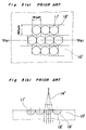
- Fig. 3 shows a refractive index distribution type flat-plate microlens array M which has been conventionally used as a condensing or converging means of projection light onto a liquid crystal panel as referred to above.
- the known flat-plate microlens array M in Fig. 3 includes a substrate 101, and a plurality of microlenses 111 formed on the substrate 101 by an ion exchange process which is one of diffusion processes so that the neighbouring microlenses may not contact each other, with the sectional shape of the refractive index distribution region being formed into approximately a semi-spherical configuration. Accordingly, an advanced line 112 of an ion diffusion region called a diffusion front of the microlenses 111 is separated as shown.
- the reason for separating the diffusion front 112 which is the boundary between the respective microlenses 111 as described above is such that it has been generally considered that rotational symmetry of the refractive distribution configuration with respect to the optical axis, which is necessary to obtain a favourable lens effect, is undesirably impaired by the fusion of the diffusion front 112, thereby to produce aberration component with directivity, thus giving rise to deterioration in the condensing characteristic of the lens.
- a microlens array comparable to that of Fig. 3 is known from US-A-4 790 632.
- the first problem is such that, even when the refractive index distribution of the microlenses 111 is in approximately a semi-spherical shape rotationally symmetrical with respect to the optical axis, if the distribution thereof in the radial direction is improper, spherical aberration tends to take place, thus adversely affecting the condensing characteristic of the lens.
- the present inventors have found, through repeated experiments and investigations that, generally in the case where a flat-plate microlens array is produced by the ion exchange method, gradient of the refractive index distribution in the vicinity of the diffusion front 112 is large, and therefore, the light incident upon the surrounding region of the microlenses 111 is excessively refracted, thus resulting in spherical aberration.
- the second problem resides in that, since the microlenses 111 are arranged so that the neighbouring ones are out of contact with each other, filling rate of the microlenses 111, i.e. ratio of the area occupied by the microlenses 111 to the total area of the microlens array substrate 101 can not be made higher than a certain limit.
- such limited filling rate may be represented by ⁇ /4 ⁇ 78.5% when circular microlenses are arranged in a square lattice shape, and by ⁇ /2 ⁇ 3 ⁇ 90.6% in the case where circular microlenses are densely arranged in a hexagonal lattice shape, but in actual practice, since the microlens arrangement must be in agreement with the pixel arrangement of the display panel, the filling rate becomes lower than the above. Since gaps among the microlenses are of an ion non-diffusion region and have no refracting function, light incident upon said region advances straight as it is, without contributing to the light condensing effect.
- the conventional flat-plate microlens array has problems with respect to the light condensing characteristic, and therefore, in the conventional projection type image display apparatus employing such flat-plate microlens array, darkness in the display image surface has not been fully improved.
- an object of the invention is to provide an image display apparatus which is high in utilization of illuminating light and capable of obtaining a bright image on the display surface by improving the condensing effect of a flat-plate microlens array for a transmission type display panel.
- Another object of the invention is to provide an image display apparatus of the above described type, which is simple in construction and stable in functioning at high accuracy.
- the invention provides an image display apparatus which comprises a display panel means having a plurality of pixel regions, and a microlens array having a plurality of microlenses arranged for converging illuminating light onto respective ones of said pixel regions, wherein said microlens array comprises a substrate having planar outer major surfaces, said microlenses being defined by variation of the refractive index of the material of said substrate, and said microlenses having boundaries which merge contiguously between neighbouring microlenses to provide, within said substrate, a contour of iso-refractive index.
- the invention provides a microlens array having a plurality of microlenses arranged for respectively converging incident light onto a plurality of pixel regions adjacent the array, said microlens array comprising a substrate having planar outer major surfaces, said microlenses being defined by variation of the refractive index of the material of said substrate, and said microlenses having boundaries which merge contiguously between neighbouring microlenses to provide, within said substrate, a contour of iso-refractive index.
- One preferred embodiment includes a flat-plate microlens array of a refractive index distribution type, which is constituted by forming a plurality of microlenses for converging illuminating light onto the respective ones of said pixel regions, on a substrate by a diffusion process, wherein diffusion fronts of the neighbouring microlenses of said flat-plate microlens array are fused into each other so as to form one continuous curved surface within said substrate.
- the configuration of the above one continuous curved surface should preferably be made so as to be suitable for the pitch of the pixels, and the pixel openings of the display panel.
- the filling rate with respect to the substrate of the microlenses shows a value close to 100%, with a consequent improvement of the condensing effect.
- the illuminating light from the light source is effectively converged by the flat-plate microlens array so as to concentratedly irradiate the pixel regions of the display panel, and thus, bright images may be obtained as compared with those of the conventional projection type image display apparatus.
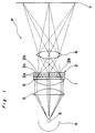
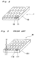
- Fig. 1 a projection type image display apparatus P according to one preferred embodiment of the present invention, with a flat-plate microlens array employed therein being shown in Fig. 2.
- the image display apparatus P includes a flat-plate microlens array 1 having a plurality of microlenses 11 formed on a substrate 10 (Fig. 2), a liquid crystal display panel 2 having a plurality of pixel regions 2b, a white light source 3 of a halogen lamp, metal halide lamp, xenon lamp or the like, a reflecting mirror 4 for reflecting light emitted from the light source 3 to be directed to said liquid crystal panel 2, condenser lenses 5 for converging the light from the light source 3, and a projecting lens 6 for projection of an image onto a projection screen 7.
- the image display apparatus P as described above is so arranged as to collect the light emitted from the light source 3, and direct it towards the projecting lens 6 through the reflecting mirror 4 and the condenser lenses 5 for projection onto the screen 7. Flux of light passing through the condenser lenses 5 is converged by the flat-plate microlens array 1 so as to be transmitted through the pixel region 2b of the liquid crystal display panel 2, and is modulated in intensity according to the image signal voltage applied to the liquid crystal layer, and thereafter, projected onto the screen 7 by the projecting lens 6.
- the above liquid crystal display panel 2 has a diagonal line of the display image surface of 75mm, pixel pitch of 190 ⁇ m (longitudinally) x 161 ⁇ m (laterally), pixel region of 88 ⁇ m (longitudinally) x 104 ⁇ m (laterally), opening rate or numerical aperture of 30%, refractive index n of the substrate at 1.53, and thickness of its substrate 2a at 1.1 mm.
- twisted nematic mode is adopted for the functioning mode of the liquid crystal, it may be replaced by any other mode so far as such mode suits the purpose.
- a polarizing plate In the functioning modes of most liquid crystals, it is required to simultaneously use a polarizing plate (not shown).
- the polarizing plate may be directly stuck onto the liquid crystal display panel, such a practice should preferably be avoided, since temperature rise following light absorption by the polarizing plate adversely affects the functioning characteristic of the liquid crystal when a light source with high brightness is employed.
- the position for disposing the polarizing plate may be at any place, provided that nothing which may vary the polarizing characteristic is inserted with respect to the liquid crystal display panel.
- the flat-plate microlens array may be inserted between the liquid crystal display panel and the polarizing plate (not shown).
- microlenses 11 referred to above are prepared by an ion exchange process as described below.
- a metallic thin film of Al, Ti, Ni, Cr or the like is formed on the surface of the glass substrate 10 by a known thin film forming technique such as the sputtering process, etc. Subsequently, very small opening windows corresponding in arrangement to that of the pixels of the liquid crystal panel 2 are formed in said metallic thin film by the known lithographic technique, thereby to provide a metallic mask.
- This glass substrate 10 is immersed for a predetermined period of time in a solution containing ion having a higher refractive index (referred to as a second ion hereinafter) than that of ion contained in said glass substrate (referred to as a first ion).
- the ion exchange is effected through the opening windows of the metallic mask, and consequently, the approximately semi-spherical microlenses 11 of the refractive index distribution type whose refractive index is gradually lowered from the vicinity of the opening windows of the metallic mask towards the peripheral portion thereof, are formed.
- the flat-plate microlens array 1 without any non-diffused region of ion over the entire surface of the glass substrate 10 may be produced by rendering the diffusion front 12 of each microlens 11 to be about 224 ⁇ m in diameter.
- Fig. 4(b) showing the state of refractive index and the state of converging of light at the cross section IV(b)-IV(b) of Fig. 4(a)
- the diffusion fronts 12 extending over the entire surface of the lens array 1 are formed into one continuous curved surface within the substrate 10.
- the refractive index gradient becomes small in the peripheral portion of each microlens 11, and light passing through the peripheral portion of the microlens is not bent due to excessive refraction, and thus, all of the light rays 14 are focused generally into one point favourably.
- each microlens 11 functions to focus light rays incident upon a hexagonal region shown by a dotted line in Fig. 4(a) (the shape of the microlens 11 shown in Fig. 2 corresponds to the shape in this region) approximately into one point favourably.
- the flat-plate microlens array 1 having such a superior condensing characteristic is installed in the state as shown in Fig. 1 through sticking by arranging positions of the respective microlenses 11 to correspond to the positions of the respective pixel regions 2b of the liquid crystal display panel 2, with the use of a transparent optical bonding agent having refractive index generally equal to that of the transparent substrate of the liquid crystal display panel.
- a conventional type flat-plate microlens array which has the lens diameter of 161 ⁇ m, and in which the diffusion fronts of the neighbouring microlenses only contact each other without fusing, was prepared as shown in Figs. 5(a) and 5(b), in which like parts in Figs. 4(a) and 4(b) are designated by like reference numerals, with addition of a prime or dash thereto for brevity of explanation.
- the brightness of the display image was about 2.5 times that in the arrangement in which the flat-plate microlens array 1 was not employed. Meanwhile, in the case where the flat-plate microlens array having the construction as in the conventional arrangement and prepared for comparison was used, the brightness of the display image was about 1.8 times that of the arrangement without using such microlens array.
- the flat-plate microlens array 1 was formed so as to provide no clearance between the microlenses 11, in the case where the microlens array is prepared to provide no clearance between the microlenses as above, the areas for the region in which the diffusion fronts of the respective microlenses are fused markedly differ according to the directions, and thus, the shape of the condensing spots is disturbed to a certain extent. In such an instance, there may be a case where a better condensing effect is obtained by slightly reducing the region in which the diffusion fronts are fused through provision of small clearances between the respective microlenses.
- the purpose of the present invention to improve condensing effect and utilization rate of illuminating light may be achieved through reduction of the spherical aberration arising from the peripheral portion of the respective microlenses by providing the diffusion region of the microlenses, and through increase of the area occupied by the microlenses with respect to the entire surface of the microlens array, etc.
- the present invention is described with reference to the Koehler illumination, the present invention may be applied to other illumination methods, e.g. critical illumination, telecentric system, etc. as well.
- the concept of the present invention is not limited in its application, to such image display apparatus alone, but may be readily applied, for example, to a system in which three liquid crystal panels are employed so as to display images of three primary colours respectively for obtaining coloured images by optically combining them.
- the display panel is not limited to the liquid crystal panel, but any other display panel of transmission type may be employed as well.
- the flat-plate microlens array 1 is prepared by the ion exchange process, it may be produced by a monomer diffusion copolymerization process, i.e. a process including the steps of preparing a transparent substrate by half-polymerization of a first monomer, providing a molecule penetration preventing mask having many openings corresponding to the arrangement of the lenses to be formed on the surface thereof, and completing the polymerization after diffusing a second monomer into the substrate through the openings of the molecule penetration preventing mask.
- a monomer diffusion copolymerization process i.e. a process including the steps of preparing a transparent substrate by half-polymerization of a first monomer, providing a molecule penetration preventing mask having many openings corresponding to the arrangement of the lenses to be formed on the surface thereof, and completing the polymerization after diffusing a second monomer into the substrate through the openings of the molecule penetration preventing mask.
- the flat-plate microlens array is formed by the semi-spherical microlenses according to the present embodiment, such microlens array may be replaced by one formed with lenticular lenses, Fresnel lens and the like.
- the shape of the microlens should preferably be determined by the pixel arrangement of the display panel and the shape of the openings of pixels, etc.
- the diffusion fronts of the neighbouring microlenses contact each other to form one continuous curved surface, not only the spherical aberration arising from the excessive refraction in the peripheral portions of the respective microlenses of the flat-plate microlens array in the conventional arrangements is reduced, but the occupying area of the microlenses with respect to the entire substrate surface of the flat-plate microlens array may be raised close to 100%, and thus, the illuminating light incident upon the display panel can be focused in the pixel region without loss for effective utilization, thereby to provide a bright projection image.
Landscapes
- Physics & Mathematics (AREA)
- General Physics & Mathematics (AREA)
- Optics & Photonics (AREA)
- Nonlinear Science (AREA)
- Chemical & Material Sciences (AREA)
- Crystallography & Structural Chemistry (AREA)
- Engineering & Computer Science (AREA)
- Manufacturing & Machinery (AREA)
- Mathematical Physics (AREA)
- Liquid Crystal (AREA)
- Devices For Indicating Variable Information By Combining Individual Elements (AREA)
Applications Claiming Priority (2)
| Application Number | Priority Date | Filing Date | Title |
|---|---|---|---|
| JP1275410A JP2641774B2 (ja) | 1989-10-23 | 1989-10-23 | 画像表示装置 |
| JP275410/89 | 1989-10-23 |
Publications (3)
| Publication Number | Publication Date |
|---|---|
| EP0425251A2 EP0425251A2 (en) | 1991-05-02 |
| EP0425251A3 EP0425251A3 (en) | 1992-03-25 |
| EP0425251B1 true EP0425251B1 (en) | 1996-04-10 |
Family
ID=17555113
Family Applications (1)
| Application Number | Title | Priority Date | Filing Date |
|---|---|---|---|
| EP90311625A Expired - Lifetime EP0425251B1 (en) | 1989-10-23 | 1990-10-23 | Image display apparatus |
Country Status (5)
| Country | Link |
|---|---|
| EP (1) | EP0425251B1 (enExample) |
| JP (1) | JP2641774B2 (enExample) |
| KR (1) | KR940006985B1 (enExample) |
| DE (1) | DE69026463T2 (enExample) |
| TW (1) | TW197498B (enExample) |
Families Citing this family (14)
| Publication number | Priority date | Publication date | Assignee | Title |
|---|---|---|---|---|
| JP2622185B2 (ja) * | 1990-06-28 | 1997-06-18 | シャープ株式会社 | カラー液晶表示装置 |
| JP2760915B2 (ja) * | 1991-06-03 | 1998-06-04 | 日本板硝子株式会社 | 画像表示装置 |
| JPH0527114A (ja) * | 1991-07-25 | 1993-02-05 | Sharp Corp | 有機カラーフイルタアレイの製造方法ならびに投影形カラー液晶表示装置 |
| DE69216340T2 (de) * | 1991-09-26 | 1997-06-26 | Canon Kk | Flüssigkristallanzeige und damit versehener Projektor |
| US5459592A (en) * | 1992-04-24 | 1995-10-17 | Sharp Kabushiki Kaisha | Projection display system including a collimating tapered waveguide or lens with the normal to optical axis angle increasing toward the lens center |
| US5499138A (en) * | 1992-05-26 | 1996-03-12 | Olympus Optical Co., Ltd. | Image display apparatus |
| JP2951858B2 (ja) * | 1994-10-17 | 1999-09-20 | シャープ株式会社 | 投影型カラー液晶表示装置 |
| US5606436A (en) * | 1994-11-21 | 1997-02-25 | Proxima Corporation | Liquid crystal projection panel construction and method of making same |
| JP3251150B2 (ja) * | 1994-12-29 | 2002-01-28 | 日本板硝子株式会社 | 平板マイクロレンズアレイおよびその製造方法 |
| WO1998033222A1 (en) * | 1997-01-27 | 1998-07-30 | Corning Incorporated | Rigid battery separator with compliant layer |
| TW459154B (en) * | 1998-11-10 | 2001-10-11 | Toshiba Corp | Flat display device |
| JP2006502439A (ja) | 2002-10-04 | 2006-01-19 | コーニング インコーポレイテッド | レンズアレイ、そのレンズアレイの製造方法および感光性ガラスプレート |
| JP2006201642A (ja) * | 2005-01-24 | 2006-08-03 | Dainippon Printing Co Ltd | 拡散レンズアレイシート、面光源装置 |
| JP2015035396A (ja) * | 2013-08-09 | 2015-02-19 | オムロン株式会社 | スイッチおよびこれを用いたキーボード |
Family Cites Families (4)
| Publication number | Priority date | Publication date | Assignee | Title |
|---|---|---|---|---|
| JPS5959421A (ja) * | 1982-09-29 | 1984-04-05 | Nippon Sheet Glass Co Ltd | プラスチツク平面レンズを製造する方法 |
| JPS60165621A (ja) * | 1984-02-08 | 1985-08-28 | Nec Corp | 透過型表示素子 |
| JPS6344624A (ja) * | 1986-08-12 | 1988-02-25 | Fuji Photo Film Co Ltd | 液晶デバイス |
| JPH01187502A (ja) * | 1988-01-22 | 1989-07-26 | Seiko Epson Corp | 平板レンズアレイ及び平板レンズアレイを備えた液晶表示素子 |
-
1989
- 1989-10-23 JP JP1275410A patent/JP2641774B2/ja not_active Expired - Lifetime
-
1990
- 1990-10-20 TW TW079108887A patent/TW197498B/zh active
- 1990-10-23 KR KR1019900016965A patent/KR940006985B1/ko not_active Expired - Fee Related
- 1990-10-23 EP EP90311625A patent/EP0425251B1/en not_active Expired - Lifetime
- 1990-10-23 DE DE69026463T patent/DE69026463T2/de not_active Expired - Lifetime
Non-Patent Citations (6)
| Title |
|---|
| PATENT ABSTRACTS OF JAPAN, vol. 10, no. 143 (P-459)(2200) 27 May 1986 & JP A 60262131 * |
| PATENT ABSTRACTS OF JAPAN, vol. 10, no. 9 (P-420)(2066) 14 January 1986 & JP A 60165622 * |
| PATENT ABSTRACTS OF JAPAN, vol. 10, no. 93 (P-445)(2150) 10 April 1986 & JP A 60227233 * |
| PATENT ABSTRACTS OF JAPAN, vol. 11, no. 303 (P-622)(2750) 3 October 1987 & JP A 62094826 * |
| PATENT ABSTRACTS OF JAPAN, vol. 13, no. 222 (P-876)(3570) 24 May 1989 & JP A 1035416 * |
| PATENT ABSTRACTS OF JAPAN, vol. 8, no. 48 (P-258)(1485) 3 March 1984 & JP A 58198001 * |
Also Published As
| Publication number | Publication date |
|---|---|
| JPH03136004A (ja) | 1991-06-10 |
| JP2641774B2 (ja) | 1997-08-20 |
| EP0425251A2 (en) | 1991-05-02 |
| EP0425251A3 (en) | 1992-03-25 |
| DE69026463D1 (de) | 1996-05-15 |
| DE69026463T2 (de) | 1996-11-28 |
| TW197498B (enExample) | 1993-01-01 |
| KR910008454A (ko) | 1991-05-31 |
| KR940006985B1 (ko) | 1994-08-03 |
Similar Documents
| Publication | Publication Date | Title |
|---|---|---|
| US5359440A (en) | Image display apparatus with microlens plate having mutually fused together lenses resulting in hexagonal shaped microlenses | |
| EP0366462B1 (en) | Projection type image display apparatus | |
| KR100262044B1 (ko) | 화상표시장치 | |
| EP0409619B1 (en) | A projection type image display apparatus | |
| US5600456A (en) | Transmission liquid crystal display with a reduced dependency of a display quality upon a visual angle | |
| EP0425251B1 (en) | Image display apparatus | |
| EP0444871B1 (en) | A projection type image display apparatus | |
| US5982552A (en) | Planar microlens array having high converging efficiency | |
| EP0598608A1 (en) | Direct-view display apparatus | |
| USRE38175E1 (en) | Liquid crystal display element and micro-lens arrangement and a display using the same | |
| EP0465171A2 (en) | A colour liquid crystal display device | |
| EP0518362B1 (en) | Image display device using liquid-crystal panel, liquid-crystal TV projector, and conical optical-element array used therein | |
| JP2552389B2 (ja) | 透過型表示装置 | |
| EP0609055A1 (en) | Light valve apparatus and display system using same | |
| JPH0430140A (ja) | 投影型カラー液晶表示装置 | |
| JP2000298201A (ja) | マイクロレンズアレイ | |
| JPH06208112A (ja) | 直視型表示装置 | |
| KR940003422B1 (ko) | 투사형 영상표시장치 | |
| KR940000591B1 (ko) | 투사형 칼라 영상표시장치 | |
| JPH0216065A (ja) | 液晶光シヤツタ | |
| JPH0962197A (ja) | 面光源素子 | |
| JPH0462532A (ja) | 投影型画像表示装置 | |
| JPH04229825A (ja) | 散乱型液晶表示デバイスを用いた画像表示装置 | |
| KR19980052197A (ko) | 액정 프로젝터의 화면 밝기 제어장치 | |
| JPH05241140A (ja) | 液晶表示装置 |
Legal Events
| Date | Code | Title | Description |
|---|---|---|---|
| PUAI | Public reference made under article 153(3) epc to a published international application that has entered the european phase |
Free format text: ORIGINAL CODE: 0009012 |
|
| 17P | Request for examination filed |
Effective date: 19901214 |
|
| AK | Designated contracting states |
Kind code of ref document: A2 Designated state(s): DE FR GB NL |
|
| PUAL | Search report despatched |
Free format text: ORIGINAL CODE: 0009013 |
|
| AK | Designated contracting states |
Kind code of ref document: A3 Designated state(s): DE FR GB NL |
|
| 17Q | First examination report despatched |
Effective date: 19931012 |
|
| GRAA | (expected) grant |
Free format text: ORIGINAL CODE: 0009210 |
|
| GRAH | Despatch of communication of intention to grant a patent |
Free format text: ORIGINAL CODE: EPIDOS IGRA |
|
| AK | Designated contracting states |
Kind code of ref document: B1 Designated state(s): DE FR GB NL |
|
| REF | Corresponds to: |
Ref document number: 69026463 Country of ref document: DE Date of ref document: 19960515 |
|
| ET | Fr: translation filed | ||
| PLBE | No opposition filed within time limit |
Free format text: ORIGINAL CODE: 0009261 |
|
| STAA | Information on the status of an ep patent application or granted ep patent |
Free format text: STATUS: NO OPPOSITION FILED WITHIN TIME LIMIT |
|
| 26N | No opposition filed | ||
| REG | Reference to a national code |
Ref country code: GB Ref legal event code: IF02 |
|
| REG | Reference to a national code |
Ref country code: GB Ref legal event code: 732E |
|
| NLS | Nl: assignments of ep-patents |
Owner name: SHARP KABUSHIKI KAISHA Effective date: 20071113 |
|
| REG | Reference to a national code |
Ref country code: FR Ref legal event code: TP |
|
| PGFP | Annual fee paid to national office [announced via postgrant information from national office to epo] |
Ref country code: DE Payment date: 20091026 Year of fee payment: 20 |
|
| PGFP | Annual fee paid to national office [announced via postgrant information from national office to epo] |
Ref country code: NL Payment date: 20091030 Year of fee payment: 20 |
|
| PGFP | Annual fee paid to national office [announced via postgrant information from national office to epo] |
Ref country code: GB Payment date: 20091021 Year of fee payment: 20 Ref country code: FR Payment date: 20091014 Year of fee payment: 20 |
|
| REG | Reference to a national code |
Ref country code: NL Ref legal event code: V4 Effective date: 20101023 |
|
| REG | Reference to a national code |
Ref country code: GB Ref legal event code: PE20 Expiry date: 20101022 |
|
| PG25 | Lapsed in a contracting state [announced via postgrant information from national office to epo] |
Ref country code: NL Free format text: LAPSE BECAUSE OF EXPIRATION OF PROTECTION Effective date: 20101023 |
|
| PG25 | Lapsed in a contracting state [announced via postgrant information from national office to epo] |
Ref country code: GB Free format text: LAPSE BECAUSE OF EXPIRATION OF PROTECTION Effective date: 20101022 |
|
| PG25 | Lapsed in a contracting state [announced via postgrant information from national office to epo] |
Ref country code: DE Free format text: LAPSE BECAUSE OF EXPIRATION OF PROTECTION Effective date: 20101023 |