EP0424944A2 - Ferroelektrische Flüssigkristallvorrichtung - Google Patents
Ferroelektrische Flüssigkristallvorrichtung Download PDFInfo
- Publication number
- EP0424944A2 EP0424944A2 EP90120500A EP90120500A EP0424944A2 EP 0424944 A2 EP0424944 A2 EP 0424944A2 EP 90120500 A EP90120500 A EP 90120500A EP 90120500 A EP90120500 A EP 90120500A EP 0424944 A2 EP0424944 A2 EP 0424944A2
- Authority
- EP
- European Patent Office
- Prior art keywords
- liquid crystal
- ferroelectric liquid
- degrees
- substrates
- alignment
- Prior art date
- Legal status (The legal status is an assumption and is not a legal conclusion. Google has not performed a legal analysis and makes no representation as to the accuracy of the status listed.)
- Granted
Links
- 239000005262 ferroelectric liquid crystals (FLCs) Substances 0.000 title claims abstract description 43
- 239000004973 liquid crystal related substance Substances 0.000 claims abstract description 73
- 239000000758 substrate Substances 0.000 claims abstract description 42
- 239000007788 liquid Substances 0.000 claims description 2
- 210000004027 cell Anatomy 0.000 description 19
- 210000002858 crystal cell Anatomy 0.000 description 14
- 239000004990 Smectic liquid crystal Substances 0.000 description 11
- VYPSYNLAJGMNEJ-UHFFFAOYSA-N Silicium dioxide Chemical compound O=[Si]=O VYPSYNLAJGMNEJ-UHFFFAOYSA-N 0.000 description 8
- 230000000052 comparative effect Effects 0.000 description 8
- 239000011810 insulating material Substances 0.000 description 7
- 230000008859 change Effects 0.000 description 6
- 230000002265 prevention Effects 0.000 description 6
- 230000005684 electric field Effects 0.000 description 5
- -1 polyparaxylylene Polymers 0.000 description 5
- 238000004140 cleaning Methods 0.000 description 4
- 238000010586 diagram Methods 0.000 description 4
- 239000011159 matrix material Substances 0.000 description 4
- 238000000034 method Methods 0.000 description 4
- 239000000377 silicon dioxide Substances 0.000 description 4
- 235000012239 silicon dioxide Nutrition 0.000 description 4
- LIVNPJMFVYWSIS-UHFFFAOYSA-N silicon monoxide Chemical compound [Si-]#[O+] LIVNPJMFVYWSIS-UHFFFAOYSA-N 0.000 description 4
- 239000004642 Polyimide Substances 0.000 description 3
- 229910052681 coesite Inorganic materials 0.000 description 3
- 230000001276 controlling effect Effects 0.000 description 3
- 229910052906 cristobalite Inorganic materials 0.000 description 3
- 230000006872 improvement Effects 0.000 description 3
- 239000000463 material Substances 0.000 description 3
- 238000005259 measurement Methods 0.000 description 3
- 229920001721 polyimide Polymers 0.000 description 3
- 230000001105 regulatory effect Effects 0.000 description 3
- 229910052682 stishovite Inorganic materials 0.000 description 3
- 229910052905 tridymite Inorganic materials 0.000 description 3
- 229910052581 Si3N4 Inorganic materials 0.000 description 2
- GWEVSGVZZGPLCZ-UHFFFAOYSA-N Titan oxide Chemical compound O=[Ti]=O GWEVSGVZZGPLCZ-UHFFFAOYSA-N 0.000 description 2
- MCMNRKCIXSYSNV-UHFFFAOYSA-N Zirconium dioxide Chemical compound O=[Zr]=O MCMNRKCIXSYSNV-UHFFFAOYSA-N 0.000 description 2
- PNEYBMLMFCGWSK-UHFFFAOYSA-N aluminium oxide Inorganic materials [O-2].[O-2].[O-2].[Al+3].[Al+3] PNEYBMLMFCGWSK-UHFFFAOYSA-N 0.000 description 2
- 230000015572 biosynthetic process Effects 0.000 description 2
- 239000011521 glass Substances 0.000 description 2
- 238000005286 illumination Methods 0.000 description 2
- 239000000203 mixture Substances 0.000 description 2
- 230000004044 response Effects 0.000 description 2
- 229910000077 silane Inorganic materials 0.000 description 2
- 238000004544 sputter deposition Methods 0.000 description 2
- 150000003609 titanium compounds Chemical class 0.000 description 2
- 238000007740 vapor deposition Methods 0.000 description 2
- 229920000178 Acrylic resin Polymers 0.000 description 1
- 239000004925 Acrylic resin Substances 0.000 description 1
- 229910052582 BN Inorganic materials 0.000 description 1
- PZNSFCLAULLKQX-UHFFFAOYSA-N Boron nitride Chemical compound N#B PZNSFCLAULLKQX-UHFFFAOYSA-N 0.000 description 1
- 229920000877 Melamine resin Polymers 0.000 description 1
- 239000004640 Melamine resin Substances 0.000 description 1
- 239000004952 Polyamide Substances 0.000 description 1
- 239000004962 Polyamide-imide Substances 0.000 description 1
- 239000004793 Polystyrene Substances 0.000 description 1
- 239000004372 Polyvinyl alcohol Substances 0.000 description 1
- 239000006087 Silane Coupling Agent Substances 0.000 description 1
- 229920001807 Urea-formaldehyde Polymers 0.000 description 1
- DHKHKXVYLBGOIT-UHFFFAOYSA-N acetaldehyde Diethyl Acetal Natural products CCOC(C)OCC DHKHKXVYLBGOIT-UHFFFAOYSA-N 0.000 description 1
- 125000002777 acetyl group Chemical class [H]C([H])([H])C(*)=O 0.000 description 1
- 239000000853 adhesive Substances 0.000 description 1
- 230000001070 adhesive effect Effects 0.000 description 1
- 125000000217 alkyl group Chemical group 0.000 description 1
- 229910052782 aluminium Inorganic materials 0.000 description 1
- 229910002113 barium titanate Inorganic materials 0.000 description 1
- 239000011324 bead Substances 0.000 description 1
- 125000000484 butyl group Chemical group [H]C([*])([H])C([H])([H])C([H])([H])C([H])([H])[H] 0.000 description 1
- 238000001354 calcination Methods 0.000 description 1
- 239000012461 cellulose resin Substances 0.000 description 1
- 229910000420 cerium oxide Inorganic materials 0.000 description 1
- QCCDYNYSHILRDG-UHFFFAOYSA-K cerium(3+);trifluoride Chemical compound [F-].[F-].[F-].[Ce+3] QCCDYNYSHILRDG-UHFFFAOYSA-K 0.000 description 1
- 229910052593 corundum Inorganic materials 0.000 description 1
- 239000013078 crystal Substances 0.000 description 1
- 230000003247 decreasing effect Effects 0.000 description 1
- 230000000694 effects Effects 0.000 description 1
- 125000001495 ethyl group Chemical group [H]C([H])([H])C([H])([H])* 0.000 description 1
- 230000008020 evaporation Effects 0.000 description 1
- 238000001704 evaporation Methods 0.000 description 1
- 239000004744 fabric Substances 0.000 description 1
- 230000005621 ferroelectricity Effects 0.000 description 1
- 238000010884 ion-beam technique Methods 0.000 description 1
- ORUIBWPALBXDOA-UHFFFAOYSA-L magnesium fluoride Chemical compound [F-].[F-].[Mg+2] ORUIBWPALBXDOA-UHFFFAOYSA-L 0.000 description 1
- 229910001635 magnesium fluoride Inorganic materials 0.000 description 1
- 238000004519 manufacturing process Methods 0.000 description 1
- 125000002496 methyl group Chemical group [H]C([H])([H])* 0.000 description 1
- 230000003287 optical effect Effects 0.000 description 1
- TWNQGVIAIRXVLR-UHFFFAOYSA-N oxo(oxoalumanyloxy)alumane Chemical compound O=[Al]O[Al]=O TWNQGVIAIRXVLR-UHFFFAOYSA-N 0.000 description 1
- BMMGVYCKOGBVEV-UHFFFAOYSA-N oxo(oxoceriooxy)cerium Chemical compound [Ce]=O.O=[Ce]=O BMMGVYCKOGBVEV-UHFFFAOYSA-N 0.000 description 1
- 239000002245 particle Substances 0.000 description 1
- 239000004033 plastic Substances 0.000 description 1
- 229920003023 plastic Polymers 0.000 description 1
- 229920003055 poly(ester-imide) Polymers 0.000 description 1
- 229920000052 poly(p-xylylene) Polymers 0.000 description 1
- 229920002647 polyamide Polymers 0.000 description 1
- 229920002312 polyamide-imide Polymers 0.000 description 1
- 229920000515 polycarbonate Polymers 0.000 description 1
- 239000004417 polycarbonate Substances 0.000 description 1
- 229920000728 polyester Polymers 0.000 description 1
- 229920002223 polystyrene Polymers 0.000 description 1
- 229920002451 polyvinyl alcohol Polymers 0.000 description 1
- 239000004800 polyvinyl chloride Substances 0.000 description 1
- 229920000915 polyvinyl chloride Polymers 0.000 description 1
- 125000001436 propyl group Chemical group [H]C([*])([H])C([H])([H])C([H])([H])[H] 0.000 description 1
- 238000007789 sealing Methods 0.000 description 1
- HBMJWWWQQXIZIP-UHFFFAOYSA-N silicon carbide Chemical compound [Si+]#[C-] HBMJWWWQQXIZIP-UHFFFAOYSA-N 0.000 description 1
- 229910010271 silicon carbide Inorganic materials 0.000 description 1
- HQVNEWCFYHHQES-UHFFFAOYSA-N silicon nitride Chemical compound N12[Si]34N5[Si]62N3[Si]51N64 HQVNEWCFYHHQES-UHFFFAOYSA-N 0.000 description 1
- 125000006850 spacer group Chemical group 0.000 description 1
- 238000002834 transmittance Methods 0.000 description 1
- 229920002554 vinyl polymer Polymers 0.000 description 1
- 229910001845 yogo sapphire Inorganic materials 0.000 description 1
Images


Classifications
-
- G—PHYSICS
- G02—OPTICS
- G02F—OPTICAL DEVICES OR ARRANGEMENTS FOR THE CONTROL OF LIGHT BY MODIFICATION OF THE OPTICAL PROPERTIES OF THE MEDIA OF THE ELEMENTS INVOLVED THEREIN; NON-LINEAR OPTICS; FREQUENCY-CHANGING OF LIGHT; OPTICAL LOGIC ELEMENTS; OPTICAL ANALOGUE/DIGITAL CONVERTERS
- G02F1/00—Devices or arrangements for the control of the intensity, colour, phase, polarisation or direction of light arriving from an independent light source, e.g. switching, gating or modulating; Non-linear optics
- G02F1/01—Devices or arrangements for the control of the intensity, colour, phase, polarisation or direction of light arriving from an independent light source, e.g. switching, gating or modulating; Non-linear optics for the control of the intensity, phase, polarisation or colour
- G02F1/13—Devices or arrangements for the control of the intensity, colour, phase, polarisation or direction of light arriving from an independent light source, e.g. switching, gating or modulating; Non-linear optics for the control of the intensity, phase, polarisation or colour based on liquid crystals, e.g. single liquid crystal display cells
- G02F1/137—Devices or arrangements for the control of the intensity, colour, phase, polarisation or direction of light arriving from an independent light source, e.g. switching, gating or modulating; Non-linear optics for the control of the intensity, phase, polarisation or colour based on liquid crystals, e.g. single liquid crystal display cells characterised by the electro-optical or magneto-optical effect, e.g. field-induced phase transition, orientation effect, guest-host interaction or dynamic scattering
- G02F1/139—Devices or arrangements for the control of the intensity, colour, phase, polarisation or direction of light arriving from an independent light source, e.g. switching, gating or modulating; Non-linear optics for the control of the intensity, phase, polarisation or colour based on liquid crystals, e.g. single liquid crystal display cells characterised by the electro-optical or magneto-optical effect, e.g. field-induced phase transition, orientation effect, guest-host interaction or dynamic scattering based on orientation effects in which the liquid crystal remains transparent
- G02F1/141—Devices or arrangements for the control of the intensity, colour, phase, polarisation or direction of light arriving from an independent light source, e.g. switching, gating or modulating; Non-linear optics for the control of the intensity, phase, polarisation or colour based on liquid crystals, e.g. single liquid crystal display cells characterised by the electro-optical or magneto-optical effect, e.g. field-induced phase transition, orientation effect, guest-host interaction or dynamic scattering based on orientation effects in which the liquid crystal remains transparent using ferroelectric liquid crystals
-
- G—PHYSICS
- G02—OPTICS
- G02F—OPTICAL DEVICES OR ARRANGEMENTS FOR THE CONTROL OF LIGHT BY MODIFICATION OF THE OPTICAL PROPERTIES OF THE MEDIA OF THE ELEMENTS INVOLVED THEREIN; NON-LINEAR OPTICS; FREQUENCY-CHANGING OF LIGHT; OPTICAL LOGIC ELEMENTS; OPTICAL ANALOGUE/DIGITAL CONVERTERS
- G02F1/00—Devices or arrangements for the control of the intensity, colour, phase, polarisation or direction of light arriving from an independent light source, e.g. switching, gating or modulating; Non-linear optics
- G02F1/01—Devices or arrangements for the control of the intensity, colour, phase, polarisation or direction of light arriving from an independent light source, e.g. switching, gating or modulating; Non-linear optics for the control of the intensity, phase, polarisation or colour
- G02F1/13—Devices or arrangements for the control of the intensity, colour, phase, polarisation or direction of light arriving from an independent light source, e.g. switching, gating or modulating; Non-linear optics for the control of the intensity, phase, polarisation or colour based on liquid crystals, e.g. single liquid crystal display cells
- G02F1/133—Constructional arrangements; Operation of liquid crystal cells; Circuit arrangements
- G02F1/1333—Constructional arrangements; Manufacturing methods
- G02F1/1337—Surface-induced orientation of the liquid crystal molecules, e.g. by alignment layers
- G02F1/133746—Surface-induced orientation of the liquid crystal molecules, e.g. by alignment layers for high pretilt angles, i.e. higher than 15 degrees
Definitions
- the present invention relates to a liquid crystal device using ferroelectric liquid crystal which can be incorporated in an image display apparatus, a recording apparatus, etc.
- Clark and Lagerwall have proposed a liquid crystal device showing bistability (U.S. Patent No. 4,367,924, etc.).
- a ferroelectric liquid crystal assuming chiral smectic C phase (SmC*) or H phase (SmH*).
- the ferroelectric liquid crystal assumes bistable states including a first optically stable state and a second optically stable state depending on the electric field thereto. Accordingly, as different from a TN-type liquid crystal used in a conventional optical modulation device, the liquid crystal is oriented to a first optically stable state in response to one electric field vector, and is oriented to a second optically stable state in response to the other electric field vector, for example.
- this type of liquid crystal has properties of quickly responding to an applied electric field to assume either one of the above-mentioned two stable states and retaining the resultant state in the absence of an electric field.
- a liquid crystal device is constituted by using a ferroelectric liquid crystal showing such properties, it is possible to obtain substantial improvements to many problems inclusive of poor viewing angle characteristic involved in a conventional TN-type device.
- the difference in directions regulated by the alignment films on a pair of substrates is too large so that the alignment axes of liquid crystal are liable to be separated into one in a region regulated by one substrate and another in a region regulated by the other substrate, thus failing to provide an increased contrast.
- An object of the present invention is to provide a liquid crystal device having solved the above-mentioned problems.
- a more specific object of the present invention is to provide a liquid crystal device including a ferroelectric liquid crystal disposed in a uniform alignment state showing bistability and a large pre-tilt angle, in which device the occurrence of two states providing a low contrast is prevented to stabilize the uniform alignment state giving a high contrast, thus resulting in an improved, and the drive margin is increased to provide a satisfactory bright-dark display under wide driving corditions.
- a ferroelectric liquid crystal device comprising a pair of substrates and a ferroelectric liquid crystal disposed between the substrates, each substrate having thereon a group of electrodes for driving the ferroelectric liquid crystal and provided with a uniaxial alignment axis for aligning the ferroelectric liquid crystal molecules; wherein the uniaxial alignment axes provided to the pair of substrates intersect each other at a prescribed intersection angle, and the liquid crystal molecules are aligned to provide a director forming a pre-tilt angle of 5 to 35 degrees with the liquid crystal aligning surfaces of the substrates.
- the uniaxial alignment axes provided to the pair of substrates intersect at a certain intersection angle ( ⁇ ) and the pre-tilt angle between the direction of liquid crystal molecules and the liquid crystal alignment surfaces is 5 degrees or larger, whereby the occurrence of a splay alignment is suppressed to provide a good alignment characteristic of the liquid crystal, thus providing a high contrast.
- ⁇ intersection angle
- the drive margin is increased, a bright- dark display over wide drive conditions to provide a stable display which is little affected by a change in threshold voltage due to an irregularity in cell thickness or a temperature change.
- Figure 1 is a block diagram showing a drive system for a liquid crystal device used in the present invention.
- Figure 2 is a plan view common to several embodiments of the ferroelectric liquid crystal device of the present invention, and Figures 3A - 3C are sectional views of the embodiments having different laminar structures respectively taken along the line A-A in Figure 2.
- the apparatus includes a ferroelectric liquid crystal device 100 according to the invention, a scanning line driver 111 as a means for applying a scanning signal to the scanning lines (electrodes) based on image signals, a data line drive 112 as a means for applying data signals to data lines (electrodes) based on the image signals to drive the ferroelectric liquid crystal device 100 in combination with the scanning line driver 111, a backlight 113 as an illumination light source, an FLC controller 114 for controlling the drive of the device 100, a power supply controller 115 as a means for supplying a power to the device 100 and the backlight 113 and a computer main body 116 for controlling the entire operation of the liquid crystal display apparatus.
- a scanning line driver 111 as a means for applying a scanning signal to the scanning lines (electrodes) based on image signals
- a data line drive 112 as a means for applying data signals to data lines (electrodes) based on the image signals to drive the ferroelectric liquid crystal device 100
- a cell structure 100 shown in Figures 2 and 3 comprises a pair of substrates 101 and 101a made of glass plates or plastic plates which are held with a predetermined gap with spacers 104 and sealed with an adhesive 106 to form a cell structure filled with a liquid crystal.
- an electrode group e.g., an electrode group for applying scanning voltages of a matrix electrode structure
- a predetermined pattern e.g., of a stripe pattern.
- another electrode group e.g., an electrode group for applying data voltages of the matrix electrode structure
- an insulating film for preventing short circuit can be formed to cover at least one side of the above-mentioned transparent electrodes 102 and 102a.
- such insulating films are not used so that alignment control films 105 and 105a are directly disposed over the transparent electrodes 102 and 102a formed on the substrates 101 and 101a, respectively.
- insulating films for short circuit prevention 109 and 109a and alignment control films 105 and 105a are disposed, respectively.
- an insulating film for short circuit prevention 109a and an alignment control film 105a are formed on the substrate 101a, and an alignment control film 105 is directly disposed on the substrate 101.
- Examples of the material constituting the alignment control films 105 and 105a may include inorganic insulating materials, such as silicon monoxide, silicon dioxide, aluminum oxide, zirconia, magnesium fluoride, cerium oxide, cerium fluoride, silicon nitride, silicon carbide, and boron nitride; and organic insulating materials, such as polyvinyl alcohol, polyimide, polyamide-imide, polyester-imide, polyparaxylylene, polyester, polycarbonate, polyvinyl acetal, polyvinyl chloride, polyamide, polystyrene, cellulose resin, melamine resin, urea resin and acrylic resin.
- inorganic insulating materials such as silicon monoxide, silicon dioxide, aluminum oxide, zirconia, magnesium fluoride, cerium oxide, cerium fluoride, silicon nitride, silicon carbide, and boron nitride
- organic insulating materials such as polyvinyl alcohol, polyimide, polyamide-imide, polyester-
- the above-mentioned alignment (control) film of an insulating material can be also used as an insulating film for short circuit prevention.
- the alignment control films 105 and 105a may preferably be formed as an inorganic insulating film which satisfactorily shows both the above-mentioned alignment control function and short circuit-preventing function. More specifically, such alignment control films 105 and 105a may for example be formed by oblique vapor deposition of an inorganic insulating material, such as SiO or SiO2 onto the substrates 101 and 101a, respectively. In this instance, the direction of the resultant uniaxial alignment axis substantially coincides with the projection of the oblique vapor deposition direction onto the substrate.
- the alignment control films 105 and 105a of an inorganic insulating material or an organic insulating material may be provided with a uniaxial alignment axis by rubbing the surface of the film after formation thereof in one direction with velvet, cloth or paper to form the uniaxial alignment axis substantially coinciding with the rubbing direction.
- the above-mentioned uniaxial alignment axes 401 and 402 are provided to the pair of substrates 101 and 101a so as to intersect each other at an intersection angle ⁇ .
- the intersection angle ⁇ can change depending on the ferroelectric liquid crystal material and the kind of the alignment control film but may preferably be selected in the range of 2 - 25 degrees.
- the pre-tilt angle ⁇ formed between the liquid crystal aligning surface 502 and the liquid crystal molecule 503 is selected in the range of 5 to 35 degrees.
- the insulating films for short circuit prevention 109 and 109a may be formed in a thickness of 200 ⁇ or larger, preferably 500 ⁇ or larger, with an inorganic insulating material, such as SiO2, TiO2, Al2O3, Si3N4 and BaTiO3.
- the film formation may for example be effected by sputtering, ion beam evaporation, or calcination of an organic titanium compound, an organic silane compound, or an organic aluminum compound.
- the organic titanium compound may for example be an alkyl (methyl, ethyl, propyl, butyl, etc.) titanate compound, and the organic silane compound may be an ordinary silane coupling agent.
- the thickness of the insulating films for short circuit prevention 109 and 109a is below 200 ⁇ , a sufficient short circuit prevention effect cannot be accomplished.
- the thickness is above 5000 ⁇ , the effective voltage applied to the liquid crystal layer is decreased substantially, so that the thickness may be set to 5000 ⁇ or less, preferably 2000 ⁇ or less.
- the liquid crystal material suitably used in the present invention is a chiral smectic liquid crystal showing ferroelectricity. More specifically, liquid crystals in chiral smectic C phase (SmC*), chiral smectic G phase (SmG*), chiral smectic F phase (SmF*), chiral smectic I phase (SmI*) or chiral smectic H phase (SmH*) may be used.
- SmC* chiral smectic C phase
- SmG* chiral smectic G phase
- SmF* chiral smectic F phase
- SmI* chiral smectic I phase
- SmH* chiral smectic H phase
- ferroelectric liquid crystals may be disclosed in, e.g., LE JOURNAL DE PHYSIQUE LETTERS 36 (L-69) 1975, "Ferroelectric Liquid Crystals”; Applied Physics Letters 36 11, 1980, “Submicro Second Bi-stable Electrooptic Switching in Liquid Crystals”; Kotai Butsuri (Solid-State Physics) 16 (141) 1981, “Ekisho (Liquid Crystals)”; U.S. Patents Nos. 4,561,726; 4,589,996; 4,592,858; 4,596,667; 4,613,209; 4,614,609; 4,622,165, etc. Chiral smectic liquid crystals disclosed in these references can be used in the present invention.
- ferroelectric liquid crystal may include decyloxybenzylidene-p′-amino-2-methylbutylcinnamate (DOBAMBC), hexyloxybenzylidene-p′-amino-2-chloropropylcinnamate (HOBACPC), and 4-O-(2-methyl)butylresorcylidene-4′-octylaniline (MBRA 8).
- DOBAMBC decyloxybenzylidene-p′-amino-2-methylbutylcinnamate
- HOBACPC hexyloxybenzylidene-p′-amino-2-chloropropylcinnamate
- MBRA 8 4-O-(2-methyl)butylresorcylidene-4′-octylaniline
- the respective polyimide alignment films were subjected to rubbing so as to be provided with rubbing axes (uniaxial alignment axes) in a relationship as will be further explained hereinafter.
- alumina beads having an average particle size of about 1.5 microns were dispersed, and the other substrate was superposed thereon so that their stripe electrodes intersected each other and their uniaxial alignment axes intersected each other at a prescribed angle ⁇ as shown in Figure 4A.
- the two substrates were fixed to each other to form a blank cell.
- the cell was then filled with a ferroelectric liquid crystal ("CS1014" (trade name), made by Chisso K.K.) under vacuum and, after sealing, the liquid crystal was gradually cooled to chiral smectic phase to be aligned.
- CS1014" trade name
- the pre-tilt angle ⁇ between the director of liquid crystal molecules and the liquid crystal aligning surfaces of the thus obtained liquid crystal cell was found to be 12 degrees as measured by the crystal rotation method (Jpn. J. Appl. Phys. Vol. 19 (1980), No. 10).
- the above-prepared matrix display cell was subjected to measurement of a drive margin under cross nicols by applying a set of driving waveforms shown in Figure 9.
- the result is also shown in Table 1.
- S N , S N+1 , S N+2 ... are shown voltage waveforms applied to the respective scanning electrodes S N , S N+1 ...; at I is shown a voltage waveform applied to a data electrode I; and at I-S N , etc. are shown voltage waveforms applied to pixel formed at the respective intersections of the scanning electrodes S N ... and the data electrode I.
- the drive margin was measured as follows.
- the set of driving waveforms shown in Figure 9 are applied to a matrix cell while changing the unit pulse width T.
- T1 as the lower limit width for giving a bright state in a normal alignment state
- T2 as the upper limit width for giving a dark state in a normal alignment state
- the drive margin is defined by (T2-T1)/(T1+T2) which increases with an increase in overlap of the ranges for writing both the bright and dark states and provides a measure of device performance.
- a liquid crystal cell was prepared in the same manner as in Examples 1 - 5 except that the intersection angle ⁇ between the rubbing axes as set to 0 degree.
- the pre-tilt ⁇ angle was measured to be 12 degrees.
- two states including a splay alignment state giving a low contrast and a uniform alignment state giving a high contrast were found.
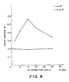
- the contrast was measured to be 10. The results are also shown in Table 1.
- Figure 6 is a schematic view illustrating positions of directors at various points between the substrates in splay and uniform alignment states.
- at 501 - 504 are respectively shown a change in director positions across the thickness, wherein a director position along a chiral smectic cone is represented by a bar projected onto the bottom (represented as a circle) of the cone as a view seen from the bottom.
- At 601 and 602 are shown two orientation states in the splay alignment
- at 603 and 604 are shown two orientation states in the uniform alignment.
- the splay alignment state and the uniform alignment state were copresent at any value of T allowing switching, thus failing to allow the switching between bright and dark states in the uniform alignment state extending over the entire picture area.
- the liquid crystal cells having a small pre-tile angle of 2.5 degrees did not provide a substantial increase in contrast ratio even at a certain intersection angle between the uniaxial alignment axes.
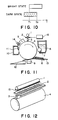
- FIG. 11 shows an electrophotographic image forming apparatus using the above liquid crystal device as a liquid crystal shutter for modulating and controlling a quantity of light to which a photosensitive member is exposed.
- Figure 12 is an enlarged perspective view showing some vital parts of the apparatus.
- the image-forming apparatus includes: an exposure lamp 1 as a light source, a liquid crystal shutter 2 of the type described above including a pair of polarizers (not specifically shown), a short-focus image forming element array 3, a photosensitive drum 4, a charger 5, a developing device 6, a developing sleeve 7, a transfer sheet guide 8, a transfer charger 9, a cleaning device 10, a cleaning blade 11, and a sheet-conveying guide.
- the photosensitive member 4 rotating in the direction of an arrow is first charged by a charger 5. Then, the photosensitive drum is illuminated with light which has been modulated depending on image data to form an electrostatic latent image thereon.
- the light modulation is effected by selectively interrupting or transmitting the light from the exposure lamp 1 through the liquid crystal shutter 2 in which the shutter elements are disposed in an array generally arranged along the axis of the photosensitive member 4.
- the shutter elements are disposed in a staggered fashion as shown so as to increase the density of the arrangement.
- the thus formed electrostatic latent image is developed by attachment of a toner charged on the developing sleeve.
- the toner image formed on the photosensitive drum 4 is transferred onto a transfer sheet 13 supplied from a paper-supply cassette (not shown) under discharge by the transfer charger 9 from the backside of the transfer sheet 13.
- the toner image on the transfer sheet 13 is then fixed by a fixing device (not shown).
- a portion of the toner remaining unused on the photosensitive drum is scraped off from the drum surface by the cleaning blade 11 to be recovered in the cleaning device 10. Further, the electric charge remaining on the photosensitive drum is extinguished by illumination with the pre-exposure lamp 14.
- a liquid crystal device comprising a ferroelectric liquid crystal disposed between a pair of substrates each provided with a uniaxial alignment axis, wherein the uniaxial alignment axes are disposed to intersect each other at a prescribed intersection angle and the pre-tilt angle between the liquid crystal molecules and the liquid crystal aligning surfaces is set to 5 - 35 degrees, whereby a good alignment characteristic is attained to provide an increased contrast ratio and also an increased drive margin is provided to allow a bright-dark display under wide driving conditions.
- a ferroelectric liquid crystal device is formed by disposing a ferroelectric liquid crystal between a pair of substrates, each having thereon a group of electrodes for driving the ferroelectric liquid crystal and provided with a uniaxial alignment axis for aligning the ferroelectric liquid crystal molecules.
- the uniaxial alignment axes provided to the pair of substrates are disposed to intersect each other at a prescribed intersection angle, and the liquid crystal molecules are aligned to provide a director forming a pre-tilt angle of 5 to 35 degrees with the liquid crystal aligning surfaces of the substrates.
- the ferroelectric liquid crystal device provides an improved contrast as well as a broad drive margin.
Landscapes
- Physics & Mathematics (AREA)
- Chemical & Material Sciences (AREA)
- Crystallography & Structural Chemistry (AREA)
- Nonlinear Science (AREA)
- General Physics & Mathematics (AREA)
- Optics & Photonics (AREA)
- Liquid Crystal (AREA)
- Liquid Crystal Substances (AREA)
Applications Claiming Priority (2)
| Application Number | Priority Date | Filing Date | Title |
|---|---|---|---|
| JP1277028A JP2645754B2 (ja) | 1989-10-26 | 1989-10-26 | 液晶素子 |
| JP277028/89 | 1989-10-26 |
Publications (3)
| Publication Number | Publication Date |
|---|---|
| EP0424944A2 true EP0424944A2 (de) | 1991-05-02 |
| EP0424944A3 EP0424944A3 (en) | 1991-09-25 |
| EP0424944B1 EP0424944B1 (de) | 1996-01-17 |
Family
ID=17577768
Family Applications (1)
| Application Number | Title | Priority Date | Filing Date |
|---|---|---|---|
| EP90120500A Expired - Lifetime EP0424944B1 (de) | 1989-10-26 | 1990-10-25 | Ferroelektrische Flüssigkristallvorrichtung |
Country Status (5)
| Country | Link |
|---|---|
| EP (1) | EP0424944B1 (de) |
| JP (1) | JP2645754B2 (de) |
| AT (1) | ATE133273T1 (de) |
| DE (1) | DE69024907T2 (de) |
| ES (1) | ES2081895T3 (de) |
Cited By (3)
| Publication number | Priority date | Publication date | Assignee | Title |
|---|---|---|---|---|
| EP0496628A2 (de) * | 1991-01-25 | 1992-07-29 | Sharp Kabushiki Kaisha | Ferroelektrische Flüssigkristall-Anzeigevorrichtung |
| EP0504911A2 (de) * | 1991-03-22 | 1992-09-23 | Canon Kabushiki Kaisha | Flüssigkristallvorrichtung |
| EP0526094A2 (de) * | 1991-07-24 | 1993-02-03 | Canon Kabushiki Kaisha | Flüssigkristallvorrichtung |
Citations (4)
| Publication number | Priority date | Publication date | Assignee | Title |
|---|---|---|---|---|
| US4591886A (en) * | 1983-07-08 | 1986-05-27 | Hitachi, Ltd. | Driving method and apparatus for optical printer with liquid-crystal switching element |
| WO1987006020A1 (en) * | 1986-04-03 | 1987-10-08 | The Secretary Of State For Defence In Her Britanni | Liquid crystal devices |
| EP0286539A1 (de) * | 1987-04-10 | 1988-10-12 | Commissariat A L'energie Atomique | Bistabile smektische ferroelektrische Flüssigkristall-Anzeigevorrichtung |
| US4778259A (en) * | 1985-07-17 | 1988-10-18 | Canon Kabushiki Kaisha | Ferroelectric liquid crystal devices having reverse twist angle and stable states resulting from A.C. excitation |
Family Cites Families (3)
| Publication number | Priority date | Publication date | Assignee | Title |
|---|---|---|---|---|
| JPH06100755B2 (ja) * | 1986-06-18 | 1994-12-12 | 日産化学工業株式会社 | 液晶セル用配向処理剤 |
| JPH0648338B2 (ja) * | 1987-04-16 | 1994-06-22 | 日産化学工業株式会社 | 液晶表示素子用配向処理剤 |
| JPH01101516A (ja) * | 1987-10-14 | 1989-04-19 | Idemitsu Kosan Co Ltd | 液晶光学素子の配向制御方法 |
-
1989
- 1989-10-26 JP JP1277028A patent/JP2645754B2/ja not_active Expired - Fee Related
-
1990
- 1990-10-25 EP EP90120500A patent/EP0424944B1/de not_active Expired - Lifetime
- 1990-10-25 DE DE69024907T patent/DE69024907T2/de not_active Expired - Fee Related
- 1990-10-25 ES ES90120500T patent/ES2081895T3/es not_active Expired - Lifetime
- 1990-10-25 AT AT90120500T patent/ATE133273T1/de not_active IP Right Cessation
Patent Citations (4)
| Publication number | Priority date | Publication date | Assignee | Title |
|---|---|---|---|---|
| US4591886A (en) * | 1983-07-08 | 1986-05-27 | Hitachi, Ltd. | Driving method and apparatus for optical printer with liquid-crystal switching element |
| US4778259A (en) * | 1985-07-17 | 1988-10-18 | Canon Kabushiki Kaisha | Ferroelectric liquid crystal devices having reverse twist angle and stable states resulting from A.C. excitation |
| WO1987006020A1 (en) * | 1986-04-03 | 1987-10-08 | The Secretary Of State For Defence In Her Britanni | Liquid crystal devices |
| EP0286539A1 (de) * | 1987-04-10 | 1988-10-12 | Commissariat A L'energie Atomique | Bistabile smektische ferroelektrische Flüssigkristall-Anzeigevorrichtung |
Cited By (8)
| Publication number | Priority date | Publication date | Assignee | Title |
|---|---|---|---|---|
| EP0496628A2 (de) * | 1991-01-25 | 1992-07-29 | Sharp Kabushiki Kaisha | Ferroelektrische Flüssigkristall-Anzeigevorrichtung |
| EP0496628A3 (en) * | 1991-01-25 | 1992-12-23 | Sharp Kabushiki Kaisha | Ferroelectric liquid crystal display device |
| US5347381A (en) * | 1991-01-25 | 1994-09-13 | Sharp Kabushiki Kaisha | Ferroelectric liquid crystal display device with molecules between hairpin and lightning defects following the lightning defects |
| EP0504911A2 (de) * | 1991-03-22 | 1992-09-23 | Canon Kabushiki Kaisha | Flüssigkristallvorrichtung |
| EP0504911A3 (en) * | 1991-03-22 | 1993-01-20 | Canon Kabushiki Kaisha | Liquid crystal device |
| US5657103A (en) * | 1991-03-22 | 1997-08-12 | Canon Kabushiki Kaisha | Liquid crystal device |
| EP0526094A2 (de) * | 1991-07-24 | 1993-02-03 | Canon Kabushiki Kaisha | Flüssigkristallvorrichtung |
| EP0526094A3 (en) * | 1991-07-24 | 1993-08-11 | Canon Kabushiki Kaisha | Liquid crystal device |
Also Published As
| Publication number | Publication date |
|---|---|
| EP0424944B1 (de) | 1996-01-17 |
| EP0424944A3 (en) | 1991-09-25 |
| ATE133273T1 (de) | 1996-02-15 |
| DE69024907D1 (de) | 1996-02-29 |
| JP2645754B2 (ja) | 1997-08-25 |
| DE69024907T2 (de) | 1996-06-05 |
| JPH03139614A (ja) | 1991-06-13 |
| ES2081895T3 (es) | 1996-03-16 |
Similar Documents
| Publication | Publication Date | Title |
|---|---|---|
| US4763995A (en) | Spacers with alignment effect and substrates having a weak alignment effect | |
| US4720173A (en) | Display having an orientation treatment between 0° and 15° to the spacer wall | |
| US4781441A (en) | Method of controlling orientation of liquid crystal, device used therein and liquid crystal device produced thereby | |
| US4738515A (en) | Driving method for liquid crystal device | |
| US4773738A (en) | Optical modulation device using ferroelectric liquid crystal and AC and DC driving voltages | |
| US4902107A (en) | Ferroelectric liquid crystal optical device having temperature compensation | |
| EP0550846B1 (de) | Ferroelektrische Flüssigkristall-Anzeigevorrichtung und Verfahren zu ihrer Herstellung | |
| EP0444705B1 (de) | Flüssigkristallelement und Flüssigkristallvorrichtung, die dieses Element verwendet | |
| US5822031A (en) | Liquid crystal device | |
| US5559616A (en) | Driving method for ferroelectric liquid crystal device with partial erasure and partial writing | |
| US5293534A (en) | Liquid crystal device | |
| US5109294A (en) | Liquid crystal apparatus having a liquid crystal panel and a panel supporting means | |
| US5646704A (en) | Chiral smectic liquid crystal device having predetermined pre-tilt angle and intersection angle | |
| EP0424944B1 (de) | Ferroelektrische Flüssigkristallvorrichtung | |
| AU673459B2 (en) | Liquid crystal device | |
| US5999157A (en) | Suppressing liquid crystal movement based on the relationship between a display pattern and a driving waveform | |
| JP2769879B2 (ja) | カイラルスメクチック液晶素子 | |
| US5293544A (en) | Liquid crystal apparatus including panel having plural bent layers of liquid crystal molecules | |
| US5956010A (en) | Liquid crystal apparatus and driving method | |
| JP2974420B2 (ja) | 強誘電性液晶素子、液晶表示素子、液晶表示装置及び記録装置 | |
| JPH0677120B2 (ja) | 液晶素子 | |
| EP0648826B1 (de) | Ferroelektrische Flüssigkristallvorrichtung und Flüssigkristallapparat | |
| JP2584235B2 (ja) | 画像形成装置及びその駆動方法 | |
| JP2983724B2 (ja) | 強誘電性液晶素子の配向処理法 | |
| JP3029179B2 (ja) | 液晶素子 |
Legal Events
| Date | Code | Title | Description |
|---|---|---|---|
| PUAI | Public reference made under article 153(3) epc to a published international application that has entered the european phase |
Free format text: ORIGINAL CODE: 0009012 |
|
| 17P | Request for examination filed |
Effective date: 19901025 |
|
| AK | Designated contracting states |
Kind code of ref document: A2 Designated state(s): AT BE CH DE DK ES FR GB GR IT LI LU NL SE |
|
| PUAL | Search report despatched |
Free format text: ORIGINAL CODE: 0009013 |
|
| AK | Designated contracting states |
Kind code of ref document: A3 Designated state(s): AT BE CH DE DK ES FR GB GR IT LI LU NL SE |
|
| 17Q | First examination report despatched |
Effective date: 19930525 |
|
| GRAA | (expected) grant |
Free format text: ORIGINAL CODE: 0009210 |
|
| AK | Designated contracting states |
Kind code of ref document: B1 Designated state(s): AT BE CH DE DK ES FR GB GR IT LI LU NL SE |
|
| PG25 | Lapsed in a contracting state [announced via postgrant information from national office to epo] |
Ref country code: GR Free format text: LAPSE BECAUSE OF FAILURE TO SUBMIT A TRANSLATION OF THE DESCRIPTION OR TO PAY THE FEE WITHIN THE PRESCRIBED TIME-LIMIT Effective date: 19960117 Ref country code: DK Effective date: 19960117 Ref country code: BE Effective date: 19960117 Ref country code: AT Effective date: 19960117 |
|
| REF | Corresponds to: |
Ref document number: 133273 Country of ref document: AT Date of ref document: 19960215 Kind code of ref document: T |
|
| ITF | It: translation for a ep patent filed | ||
| REF | Corresponds to: |
Ref document number: 69024907 Country of ref document: DE Date of ref document: 19960229 |
|
| REG | Reference to a national code |
Ref country code: CH Ref legal event code: NV Representative=s name: BOVARD AG PATENTANWAELTE |
|
| REG | Reference to a national code |
Ref country code: ES Ref legal event code: FG2A Ref document number: 2081895 Country of ref document: ES Kind code of ref document: T3 |
|
| ET | Fr: translation filed | ||
| PG25 | Lapsed in a contracting state [announced via postgrant information from national office to epo] |
Ref country code: LU Free format text: LAPSE BECAUSE OF NON-PAYMENT OF DUE FEES Effective date: 19961031 |
|
| PLBE | No opposition filed within time limit |
Free format text: ORIGINAL CODE: 0009261 |
|
| STAA | Information on the status of an ep patent application or granted ep patent |
Free format text: STATUS: NO OPPOSITION FILED WITHIN TIME LIMIT |
|
| 26N | No opposition filed | ||
| REG | Reference to a national code |
Ref country code: GB Ref legal event code: IF02 |
|
| PGFP | Annual fee paid to national office [announced via postgrant information from national office to epo] |
Ref country code: SE Payment date: 20021004 Year of fee payment: 13 |
|
| PGFP | Annual fee paid to national office [announced via postgrant information from national office to epo] |
Ref country code: FR Payment date: 20021008 Year of fee payment: 13 |
|
| PGFP | Annual fee paid to national office [announced via postgrant information from national office to epo] |
Ref country code: GB Payment date: 20021023 Year of fee payment: 13 |
|
| PGFP | Annual fee paid to national office [announced via postgrant information from national office to epo] |
Ref country code: NL Payment date: 20021031 Year of fee payment: 13 Ref country code: ES Payment date: 20021031 Year of fee payment: 13 Ref country code: DE Payment date: 20021031 Year of fee payment: 13 |
|
| PGFP | Annual fee paid to national office [announced via postgrant information from national office to epo] |
Ref country code: CH Payment date: 20021101 Year of fee payment: 13 |
|
| PG25 | Lapsed in a contracting state [announced via postgrant information from national office to epo] |
Ref country code: GB Free format text: LAPSE BECAUSE OF NON-PAYMENT OF DUE FEES Effective date: 20031025 |
|
| PG25 | Lapsed in a contracting state [announced via postgrant information from national office to epo] |
Ref country code: SE Free format text: LAPSE BECAUSE OF NON-PAYMENT OF DUE FEES Effective date: 20031026 |
|
| PG25 | Lapsed in a contracting state [announced via postgrant information from national office to epo] |
Ref country code: ES Free format text: LAPSE BECAUSE OF NON-PAYMENT OF DUE FEES Effective date: 20031027 |
|
| PG25 | Lapsed in a contracting state [announced via postgrant information from national office to epo] |
Ref country code: LI Free format text: LAPSE BECAUSE OF NON-PAYMENT OF DUE FEES Effective date: 20031031 Ref country code: CH Free format text: LAPSE BECAUSE OF NON-PAYMENT OF DUE FEES Effective date: 20031031 |
|
| PG25 | Lapsed in a contracting state [announced via postgrant information from national office to epo] |
Ref country code: NL Free format text: LAPSE BECAUSE OF NON-PAYMENT OF DUE FEES Effective date: 20040501 Ref country code: DE Free format text: LAPSE BECAUSE OF NON-PAYMENT OF DUE FEES Effective date: 20040501 |
|
| EUG | Se: european patent has lapsed | ||
| REG | Reference to a national code |
Ref country code: CH Ref legal event code: PL |
|
| GBPC | Gb: european patent ceased through non-payment of renewal fee |
Effective date: 20031025 |
|
| PG25 | Lapsed in a contracting state [announced via postgrant information from national office to epo] |
Ref country code: FR Free format text: LAPSE BECAUSE OF NON-PAYMENT OF DUE FEES Effective date: 20040630 |
|
| NLV4 | Nl: lapsed or anulled due to non-payment of the annual fee |
Effective date: 20040501 |
|
| REG | Reference to a national code |
Ref country code: FR Ref legal event code: ST |
|
| REG | Reference to a national code |
Ref country code: ES Ref legal event code: FD2A Effective date: 20031027 |
|
| PG25 | Lapsed in a contracting state [announced via postgrant information from national office to epo] |
Ref country code: IT Free format text: LAPSE BECAUSE OF NON-PAYMENT OF DUE FEES;WARNING: LAPSES OF ITALIAN PATENTS WITH EFFECTIVE DATE BEFORE 2007 MAY HAVE OCCURRED AT ANY TIME BEFORE 2007. THE CORRECT EFFECTIVE DATE MAY BE DIFFERENT FROM THE ONE RECORDED. Effective date: 20051025 |