EP0424889A2 - A memory management system for reallocating memory space based on data set in registers - Google Patents
A memory management system for reallocating memory space based on data set in registers Download PDFInfo
- Publication number
- EP0424889A2 EP0424889A2 EP90120339A EP90120339A EP0424889A2 EP 0424889 A2 EP0424889 A2 EP 0424889A2 EP 90120339 A EP90120339 A EP 90120339A EP 90120339 A EP90120339 A EP 90120339A EP 0424889 A2 EP0424889 A2 EP 0424889A2
- Authority
- EP
- European Patent Office
- Prior art keywords
- memory
- address
- address space
- cpu
- bits
- Prior art date
- Legal status (The legal status is an assumption and is not a legal conclusion. Google has not performed a legal analysis and makes no representation as to the accuracy of the status listed.)
- Withdrawn
Links
Images


Classifications
-
- G—PHYSICS
- G06—COMPUTING; CALCULATING OR COUNTING
- G06F—ELECTRIC DIGITAL DATA PROCESSING
- G06F12/00—Accessing, addressing or allocating within memory systems or architectures
- G06F12/02—Addressing or allocation; Relocation
-
- G—PHYSICS
- G06—COMPUTING; CALCULATING OR COUNTING
- G06F—ELECTRIC DIGITAL DATA PROCESSING
- G06F12/00—Accessing, addressing or allocating within memory systems or architectures
- G06F12/02—Addressing or allocation; Relocation
- G06F12/0223—User address space allocation, e.g. contiguous or non contiguous base addressing
- G06F12/0292—User address space allocation, e.g. contiguous or non contiguous base addressing using tables or multilevel address translation means
Landscapes
- Engineering & Computer Science (AREA)
- Theoretical Computer Science (AREA)
- Physics & Mathematics (AREA)
- General Engineering & Computer Science (AREA)
- General Physics & Mathematics (AREA)
- Memory System (AREA)
- Techniques For Improving Reliability Of Storages (AREA)
Abstract
A part of a CPU address space is divided into a plurality of blocks, and registers (11) are provided for each of the divided blocks. The upper bits of location data in the CPU address data where the divided block is reallocated are set in the registers. The values set in the respective registers are compared with the address of predetermined number of bits from the CPU by the comparators (12). A coincidence signal is output to the selector 14 from the comparator where the coincidence is obtained. In response to the coincidence signal, the selector 14 outputs the upper bits of the corresponding address of the corresponding memory address space. The upper bits are combined with the lower bits of the address data from the CPU to be supplied to a memory (16) as a memory address.
Description
- The present invention relates to a memory management system adapted to a personal computer.
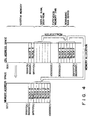
- In a conventional personal computer, an address space managed by a CPU is comprised of a RAM area serving as a system memory, a ROM area storing a BIOS (basic input and output system) and the like, a video RAM area, and an area related to a user for allocating an extension memory. A conventional memory map is shown in Fig. 1. In Fig. 1, the system memory is allocated in addresses 0(h) through 9FFFF(h) (h represents a hexadecimal). The video RAM area is allocated in the address A0000(h) through BFFFF(h). A dedicated RAM which is independent of the system memory and is managed by a display circuit is allocated to the video RAM area. The addresses C0000(h) through EFFFF(h) are released to permit a user to mount an extension ROM or an interface with a peripheral unit. The BIOS-ROM is allocated in addresses F0000(h) through FFFFF(h). Further, the extension memory is allocated in the address 100000(h) or more.
- Recently, the capacity of RAM is increased and a RAM of 1M (mega) bits or more has been used. For example, 8 1M-bit RAMs can constitute 1MB (mega byte) memory space.
- An industrial standard machine usually supports a system memory address space of 640 Kbytes (or 512K bytes). The address space from 640 KB (512KB) to 1MB is assigned to the BIOS ROM and the video RAM. Accordingly, if the system memory ranging from 0(h) through 9FFFF(h) in the memory map described above is constituted by using the 1M-bit RAM, a memory capacity of 384 KB (512KB) ranging from A0000(h) through FFFFF(h) is redundant. This redundant memory is usually reallocated in the address 100000(h) or more under the control of the address decoding conditions to thereby effectively use the redundant memory. Since the extension memory or the like may be allocated in the address 100000(h) or more, the control is required for avoiding the redundant memory being allocated overlapped with the extension memory.
- In a conventional system, the memory size of the extension memory is limited to 1MB, 4MB, and 8MB. In accordance with the selection of 2MB, 4MB, and 8MB, the memory address to be reallocated is controlled by a logic circuit constituted by a gate array. Accordingly, the addresses to be reallocatable are preliminarily fixed, resulting in limited combinations of the extension memory size and the reallocation address.
- Accordingly, the memory extension is limited to fixed combinations. Even if a new memory having a capacity other than that of the existing memories is developed in the near future, the logic circuit is not designed to take account of it. Thus, the new memory cannot be used as the extension memory.
- If the capacity of the system memory is designed to be changeable, i.e., if the system memory is allocated in the addresses from 0(h) through 7FFFF(h), the memory of 512KB becomes redundant. In this case, the address control of further 128KB (512KB-384KB) in addition to 384KB must be controlled by the hardware logic.
- The more flexible a memory arrangement or a memory allocation, the more sophisticated the hardware arrangement. More specifically, the memory arrangement and the hardware arrangement can only be selected from the combinations preliminarily determined by the hardware.
- An object of the present invention is to provide a memory management system in which a part of a CPU address space is reallocatable in an arbitrary location of the CPU address space.
- In order to achieve the above object, a memory management system according to the present invention comprises: means, provided for each divided blocks of a logical address space, for storing data indicating location where the block is reallocated; means for setting, in said storage means, an arbitrary location data in the logical address space; and allocating means for allocating the corresponding block in a physical address space based on the location data set in said storage means.
- According to the present invention, a part of the CPU address space (a logical address space) is divided into a plurality of blocks. Registers are provided to the divided blocks in one-to-one correspondence. Arbitrary location addresses in the CPU address space where the blocks are to be reallocated in a memory address space (physical address space) based on the location data reallocated in the CPU address space. Accordingly, size of the extension memory is not constrained. Further, the size of the system memory can be arbitrary set by setting adequate reallocation data in the registers. A logic circuit must not be preliminarily designed taking account of the effective arrangement of the extension memory and the size of the system memory.
- This invention can be more fully understood from the following detailed description when taken in con junction with the accompanying drawings, in which:
- Fig. 1 is a conventional memory map illustrating an example of an address space viewed from a CPU;
- Fig. 2 is a block diagram showing an example of a memory management system of the present invention;
- Fig. 3 is a table indicating addresses in the CPU address space to be set in the registers;
- Fig. 4 is a memory map after a part of the address space viewed from a CPU is reallocated in the CPU address space; and
- Fig. 5 is a conceptual view showing a conversion from a CPU address (logical address) to a memory address (physical address).
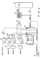
- Fig. 2 is a block diagram showing an embodiment of a memory management system according to the present invention. In this embodiment, the size of a memory (RAM) 16 is 1MB (mega bytes) and a first 512KB memory is unconditionally assigned to the CPU addresses 0(h) through 7FFFF(h). The remaining 512KB memory is divided into 8 blocks (
block 8,block 9, ..., block F) each having 64KB memory capacity. (see Fig. 4) Accordingly, the 20-bit memory address is enough to access thememory 16.Registers 11 are provided for each block in one-to-one correspondence. The respective registers store data indicating locations where the corresponding blocks (a part of the CPU address space, i.e., a logical address space) are to be reallocated in the CPU address space. The location data is set by an initialize routine in the BIOS, for example. - In this embodiment, the
CPU 31 is comprised of a 32-bit microprocessor 80386SX manufactured by an Intel. Corp., U.S.A. In this case, the address output from theCPU 31 is a 24-bit data. On the other hand, the memory address space is 1MB, the memory address is a 20 bit data. Accordingly, when the CPU address is converted into the memory address, the lower 16 bits of the CPU address are same as those of the memory address. Therefore, the upper 8 bits of the CPU address are converted into the upper 4 bits of the memory address. Accordingly, the upper 8 bits (bit 16 through bit 23) of the address data (24 bits) for reallocating the divided block into an arbitrary location in the CPU address space, are set in theregisters 11, individually. For example, as shown in Fig. 4, when theblocks registers 11, respectively corresponding to theblocks 8 through F. - The outputs of the
respective registers 11 are supplied to the respective one input terminals ofcomparators 12, and the upper 8 bits of the address data output from theCPU 31 is supplied to the other terminal of each of thecomparator 12. Thecomparator 12 compare the upper 8 bits from theCPU 31 with the upper 8 bits from theregisters 11. When a coincidence is obtained from any one of thecomparators 12, it outputs a logic "1" signal. The output signals from thecomparators 12 are supplied to the one input terminals of theAND gates 23. Further, an output signal of a comparator 21 is supplied to the other terminal of each of theAND gate 23. The comparator 21 detects whether the address of the upper 8 bits supplied from theCPU 31 coincides with the address of the system memory, i.e., "00"(h) through "07"(h). Upon detecting the coincidence, the comparator 21 outputs the logic "0" signal to theAND gate 23 and logic "1" signal to aselector 14. Accordingly, when the upper 8 bits of "00"(h) through "07"(h) of the CPU addresses "0"(h) through "7FFFF"(h) are set in theregister 11, the coincidence signal of logic "1" output from thecomparator 12 is gated by theAND gate 23. - The respective outputs from the
AND gate 23 are supplied to theselector 14 as well as to anOR gate 13. The upper 4 bits ("8"(h) through "F"(h)) of the memory address space ("80000"(h) through "FFFFF"(h) excluding "0"(h) through "7FFFF"(h)) are fixedly supplied to theselector 14. Furthermore, the four bits ofbit 16 throughbit 19 among the address output from theCPU 31 are supplied to theselector 14. In response to the logic "1" signal from the comparator 21, theselector 14 outputs thebits 16 through 19 of the CPU address. When the logic "1" signal is output from the ANDgate 23 of theblock 8, theselector 14 outputs the upper 4 bits ("8"(h)) of the memory address. When the logic "1" signal is output from the ANDgate 23 of theblock 9, theselector 14 outputs the upper 4 bits "9"(h) of the memory address. Similarly, when the logic "1" signal is output from the ANDgates 23 of the blocks A through F, theselector 14 outputs the upper 4 bits of "A"(h) through "F"(h). The upper 4 bits output from theselector 14 is combined with the lower 16 bits (bit 0 through bit 15) supplied from theCPU 31 to be supplied to theRAM 16 as well as thememory controller 15 as the 20-bit memory address. Accordingly, when the address output from theCPU 31 indicates any one of theblocks 0 through 7 in the CPU address space, theselector 14 directly, outputs the CPU address as the memory address. Further, when the address output from theCPU 31 indicates the blocks any one of theblocks 8 through F in the CPU address space, theselector 14 outputs the corresponding 4 bits of "A0000"(h) through "100000"(h) in the memory address space. The concept of converting the CPU address into the memory address is shown in Fig. 5. - The output signal from the
OR gate 12 is further supplied to thememory controller 15. The OR gate outputs data to thememory controller 15 indicating that any one of the blocks "8" through "F" is accessed by theCPU 31. Based on the output signal from theOR gate 13 and the memory address from theselector 14, thememory controller 15 which has been known outputs memory control signals such as an address strobe signal (RAS), and a column address strobe signal (CAS). - An operation of the memory management system according to the present invention constructed as above will now be described.
- First, in the initialize routine of BIOS, the different addresses where the 8 divided blocks from
block 8 through block F are to be reallocated in the CPU address space are set in theregisters 11. In this embodiment, the system memory has 512KB in size and no other memories such as the video RAM and the BIOS ROM are allocated in the 128KB memory space ranging from 512KB to 640KB. Accordingly, blocks 8 and 9 are reallocated in the addresses "80000"(h) through "9FFFF"(h) in the CPU address space. Further, the upper 8-bit data of "08"(h) and "09"(h) are set in the corresponding registers 11. The blocks A through F ranging from the addresses "A0000"(h) through "100000"(h) in the CPU address space are reallocated in the addresses "300000"(h) through "35FFFF"(h). Accordingly, "30"(h), "31"(h), "32"(h), "33"(h), "34"(h), and "35"(h) are set in thecorresponding registers 11, respectively. - When the system memory address (CPUA23-0) in the CPU address space is output from the
CPU 31, the upper 8 bits of the address are supplied to the one input terminal of the comparator 21. Furthermore, the upper 4 bits ("0"(h) through "7"(h)) of the system memory address are fixedly supplied to the other input terminal of the comparator 21. Accordingly, the coincidence signal is output from the comparator 21, inverted by aninverter 25, and then supplied to theselector 14 as logic "1" signal. As a result, the bits 19-16 are combined with the lower 16 bits (CPUA15-0) output from theCPU 31 and supplied to theRAM 16 as the memory address (MA19-0). As a result, the location in theRAM 16 designated by the memory address is accessed under the control of thememory controller 15. - On the other hand, when any one of the addresses ranging from "80000"(h) to "9FFFF"(h) and "300000"(h) to "35FFFF"(h) is output, the upper 8 bits thereof are output to the comparator 21 and the
corresponding comparator 12. In this case, the logic "1" signal from the comparator 21 is inverted to logic "0" by theinverter 25 and then supplied to theselector 14. Further, the coincidence signal of logic "1" signal from the correspondingcomparator 12 is output to theselector 14. In response to the coincidence signal, theselector 14 outputs the upper four bits (MA19-16) of the corresponding memory address. For example, when the address "300000"(h) is output from theCPU 31, the upper 8 bits "30"(h) thereof is compared with the "30"(h) from the correspondingregister 11 by the correspondingcomparator 12. As a result, the coincidence signal is supplied to theselector 14 from the correspondingcomparator 12. Accordingly, the upper 4 bits "8"(h) of the memory address is output from theselector 14. This address (MA19-16) is combined with the address (CPUA 15-0) output from theCPU 31 and then supplied to theRAM 16 as the 20-bit memory address. Thus, the location designated by the memory address is accessed under the control of the control signals from thememory controller 15. - The present invention is not limited to the above embodiment. For example, the address ranging from "0"(h) through "7FFFF"(h) is fixedly used as the system memory. However, the above address range may be blocked if necessary. Further, the address range of the system memory is compared by the comparator 21. However, a flip-flop (flag) may be set and the output thereof may be supplied to the
selector 14.
Claims (7)
1. A memory management system, comprising:
means (11), provided for each divided blocks of a logical address space, for storing data indicating locations where the block is reallocated;
means (31) for setting, in said storage means, an arbitrary location data in the logical address space;
and allocating means (13, 14, 25, 27, 15) for allocating the corresponding block in a physical address space based on the location data set in said storage means.
2. The system according to claim 1, characterized in that said storage means is provided for each of the blocks, the different values being set in the storage means.
3. The system according to claim 2, characterized in that said allocating means includes, corresponding to the respective storage means for comparing predetermined number of bits of an address supplied from a central processing unit (CPU) with the value set in the register, outputs, upon coincidence is obtained by any one of the comparing means, address data within the physical address space corresponding to location in the logical address space set in the corresponding storage means, and supplies the address data to a memory address of predetermined bits supplied from the CPU as the memory address.
4. The system according to claim 1, characterized in that the physical address space is expanded by an extension memory of an arbitrary size.
5. The system according to claim 1, characterized by further comprising means for dividing into a plurality of blocks the remaining physical address space excluding the logical address space used as the system memory among the logical address space.
6. The system according to claim 1, characterized in that the setting of the location data into the storage means is performed by a program.
7. The system according to claim 1, characterized in that the logical address is a CPU address and the physical address is a memory address space.
Applications Claiming Priority (2)
| Application Number | Priority Date | Filing Date | Title |
|---|---|---|---|
| JP1274967A JPH03137744A (en) | 1989-10-24 | 1989-10-24 | Memory control system |
| JP274967/89 | 1989-10-24 |
Publications (2)
| Publication Number | Publication Date |
|---|---|
| EP0424889A2 true EP0424889A2 (en) | 1991-05-02 |
| EP0424889A3 EP0424889A3 (en) | 1991-11-27 |
Family
ID=17549068
Family Applications (1)
| Application Number | Title | Priority Date | Filing Date |
|---|---|---|---|
| EP19900120339 Withdrawn EP0424889A3 (en) | 1989-10-24 | 1990-10-23 | A memory management system for reallocating memory space based on data set in registers |
Country Status (3)
| Country | Link |
|---|---|
| EP (1) | EP0424889A3 (en) |
| JP (1) | JPH03137744A (en) |
| KR (1) | KR930002313B1 (en) |
Cited By (1)
| Publication number | Priority date | Publication date | Assignee | Title |
|---|---|---|---|---|
| US7603593B2 (en) | 2004-06-14 | 2009-10-13 | Massimo Iaculo | Method for managing bad memory blocks in a nonvolatile-memory device, and nonvolatile-memory device implementing the management method |
Citations (2)
| Publication number | Priority date | Publication date | Assignee | Title |
|---|---|---|---|---|
| EP0200440A2 (en) * | 1985-04-30 | 1986-11-05 | Ing. C. Olivetti & C., S.p.A. | Electronic circuit for connecting a processor to a high-capacity memory |
| WO1988006761A1 (en) * | 1987-03-03 | 1988-09-07 | Tandon Corporation | Computer system providing address modification and accommodating dma and interrupts |
-
1989
- 1989-10-24 JP JP1274967A patent/JPH03137744A/en active Pending
-
1990
- 1990-10-23 EP EP19900120339 patent/EP0424889A3/en not_active Withdrawn
- 1990-10-24 KR KR9017005A patent/KR930002313B1/en not_active IP Right Cessation
Patent Citations (2)
| Publication number | Priority date | Publication date | Assignee | Title |
|---|---|---|---|---|
| EP0200440A2 (en) * | 1985-04-30 | 1986-11-05 | Ing. C. Olivetti & C., S.p.A. | Electronic circuit for connecting a processor to a high-capacity memory |
| WO1988006761A1 (en) * | 1987-03-03 | 1988-09-07 | Tandon Corporation | Computer system providing address modification and accommodating dma and interrupts |
Non-Patent Citations (2)
| Title |
|---|
| ELECTRON. & APPLIC. INDUSTR., no. 261, December 1978, pages 29-31; J.-C. MATHON: "La banque de données à microprocesseur" * |
| WESCON CONFERENCE RECORD, vol. 25, September 1981, pages 1-8 (9/4), El Segundo, CA, US; L. HUNTER: "Implementing a virtual memory system using the MC68451 memory management unit" * |
Cited By (1)
| Publication number | Priority date | Publication date | Assignee | Title |
|---|---|---|---|---|
| US7603593B2 (en) | 2004-06-14 | 2009-10-13 | Massimo Iaculo | Method for managing bad memory blocks in a nonvolatile-memory device, and nonvolatile-memory device implementing the management method |
Also Published As
| Publication number | Publication date |
|---|---|
| KR930002313B1 (en) | 1993-03-29 |
| JPH03137744A (en) | 1991-06-12 |
| KR910008574A (en) | 1991-05-31 |
| EP0424889A3 (en) | 1991-11-27 |
Similar Documents
| Publication | Publication Date | Title |
|---|---|---|
| EP0473275B1 (en) | Memory control unit and memory unit | |
| US4835734A (en) | Address translation apparatus | |
| EP0387644A1 (en) | Multiprocessor system with global data replication and two levels of address translation units | |
| EP0187453B1 (en) | Program assignable i/o addresses for a computer | |
| US4737909A (en) | Cache memory address apparatus | |
| KR940001877B1 (en) | Multiprocessor system | |
| US6226736B1 (en) | Microprocessor configuration arrangement for selecting an external bus width | |
| US4608632A (en) | Memory paging system in a microcomputer | |
| US5132927A (en) | System for cache space allocation using selective addressing | |
| US6625673B1 (en) | Method for assigning addresses to input/output devices | |
| EP0214490A2 (en) | Data processing apparatus with a virtual storage address boundary check circuit | |
| US5761719A (en) | On-chip memory map for processor cache macro | |
| EP0424889A2 (en) | A memory management system for reallocating memory space based on data set in registers | |
| WO1996017304A1 (en) | Bus-to-bus bridge | |
| US5247631A (en) | Programmable control of EMS page register addresses | |
| JPH0148570B2 (en) | ||
| JPS6232516B2 (en) | ||
| US5410662A (en) | Programmable control of EMS page register addresses | |
| JPH06175917A (en) | Flash memory | |
| JPH02245840A (en) | Storage device | |
| JP3449749B2 (en) | Information processing device | |
| KR890000805B1 (en) | Memory space mapping system | |
| JPH01140342A (en) | Virtual computer system | |
| JPH04237348A (en) | Memory accessing device | |
| JPH02183845A (en) | Control circuit for add-on memory |
Legal Events
| Date | Code | Title | Description |
|---|---|---|---|
| PUAI | Public reference made under article 153(3) epc to a published international application that has entered the european phase |
Free format text: ORIGINAL CODE: 0009012 |
|
| 17P | Request for examination filed |
Effective date: 19901120 |
|
| AK | Designated contracting states |
Kind code of ref document: A2 Designated state(s): DE FR GB |
|
| PUAL | Search report despatched |
Free format text: ORIGINAL CODE: 0009013 |
|
| AK | Designated contracting states |
Kind code of ref document: A3 Designated state(s): DE FR GB |
|
| STAA | Information on the status of an ep patent application or granted ep patent |
Free format text: STATUS: THE APPLICATION HAS BEEN WITHDRAWN |
|
| 18W | Application withdrawn |
Withdrawal date: 19930526 |