EP0422375A2 - Allgemeine Ätz-Stoppschichten aus Salzen von polyamischer Säure für reaktives ionisches Ätzen - Google Patents
Allgemeine Ätz-Stoppschichten aus Salzen von polyamischer Säure für reaktives ionisches Ätzen Download PDFInfo
- Publication number
- EP0422375A2 EP0422375A2 EP90116541A EP90116541A EP0422375A2 EP 0422375 A2 EP0422375 A2 EP 0422375A2 EP 90116541 A EP90116541 A EP 90116541A EP 90116541 A EP90116541 A EP 90116541A EP 0422375 A2 EP0422375 A2 EP 0422375A2
- Authority
- EP
- European Patent Office
- Prior art keywords
- layer
- polyamic acid
- anyone
- ions
- group
- Prior art date
- Legal status (The legal status is an assumption and is not a legal conclusion. Google has not performed a legal analysis and makes no representation as to the accuracy of the status listed.)
- Granted
Links
- 229920005575 poly(amic acid) Polymers 0.000 title claims abstract description 51
- 230000004888 barrier function Effects 0.000 title claims abstract description 16
- 150000003839 salts Chemical class 0.000 title abstract description 23
- 238000000034 method Methods 0.000 claims abstract description 41
- 239000007789 gas Substances 0.000 claims abstract description 26
- 229920000642 polymer Polymers 0.000 claims abstract description 23
- 239000000463 material Substances 0.000 claims abstract description 22
- 150000001768 cations Chemical class 0.000 claims description 33
- 239000000758 substrate Substances 0.000 claims description 30
- 238000001020 plasma etching Methods 0.000 claims description 21
- QVGXLLKOCUKJST-UHFFFAOYSA-N atomic oxygen Chemical compound [O] QVGXLLKOCUKJST-UHFFFAOYSA-N 0.000 claims description 15
- 239000001301 oxygen Substances 0.000 claims description 15
- 229910052760 oxygen Inorganic materials 0.000 claims description 15
- XUIMIQQOPSSXEZ-UHFFFAOYSA-N Silicon Chemical compound [Si] XUIMIQQOPSSXEZ-UHFFFAOYSA-N 0.000 claims description 12
- 229910052751 metal Inorganic materials 0.000 claims description 12
- 239000002184 metal Substances 0.000 claims description 12
- 229910052710 silicon Inorganic materials 0.000 claims description 12
- 239000010703 silicon Substances 0.000 claims description 12
- 229910052736 halogen Inorganic materials 0.000 claims description 10
- 150000002500 ions Chemical class 0.000 claims description 10
- 150000002367 halogens Chemical class 0.000 claims description 9
- 229910052709 silver Inorganic materials 0.000 claims description 9
- 239000004332 silver Substances 0.000 claims description 9
- PXHVJJICTQNCMI-UHFFFAOYSA-N Nickel Chemical compound [Ni] PXHVJJICTQNCMI-UHFFFAOYSA-N 0.000 claims description 8
- 229910021645 metal ion Inorganic materials 0.000 claims description 8
- -1 CC2F2 Chemical compound 0.000 claims description 7
- RYGMFSIKBFXOCR-UHFFFAOYSA-N Copper Chemical compound [Cu] RYGMFSIKBFXOCR-UHFFFAOYSA-N 0.000 claims description 7
- 229910052802 copper Inorganic materials 0.000 claims description 7
- 239000010949 copper Substances 0.000 claims description 7
- GTDPSWPPOUPBNX-UHFFFAOYSA-N ac1mqpva Chemical compound CC12C(=O)OC(=O)C1(C)C1(C)C2(C)C(=O)OC1=O GTDPSWPPOUPBNX-UHFFFAOYSA-N 0.000 claims description 6
- OYPRJOBELJOOCE-UHFFFAOYSA-N Calcium Chemical compound [Ca] OYPRJOBELJOOCE-UHFFFAOYSA-N 0.000 claims description 5
- 239000011575 calcium Substances 0.000 claims description 5
- 229910052791 calcium Inorganic materials 0.000 claims description 5
- 239000011133 lead Substances 0.000 claims description 5
- 229910001385 heavy metal Inorganic materials 0.000 claims description 4
- 229910052759 nickel Inorganic materials 0.000 claims description 4
- VYZAMTAEIAYCRO-UHFFFAOYSA-N Chromium Chemical compound [Cr] VYZAMTAEIAYCRO-UHFFFAOYSA-N 0.000 claims description 3
- FYYHWMGAXLPEAU-UHFFFAOYSA-N Magnesium Chemical compound [Mg] FYYHWMGAXLPEAU-UHFFFAOYSA-N 0.000 claims description 3
- 125000003118 aryl group Chemical group 0.000 claims description 3
- 229910052804 chromium Inorganic materials 0.000 claims description 3
- 239000011651 chromium Substances 0.000 claims description 3
- 239000010941 cobalt Substances 0.000 claims description 3
- GUTLYIVDDKVIGB-UHFFFAOYSA-N cobalt atom Chemical compound [Co] GUTLYIVDDKVIGB-UHFFFAOYSA-N 0.000 claims description 3
- 229910052749 magnesium Inorganic materials 0.000 claims description 3
- 239000011777 magnesium Substances 0.000 claims description 3
- PWHULOQIROXLJO-UHFFFAOYSA-N Manganese Chemical compound [Mn] PWHULOQIROXLJO-UHFFFAOYSA-N 0.000 claims description 2
- RTAQQCXQSZGOHL-UHFFFAOYSA-N Titanium Chemical compound [Ti] RTAQQCXQSZGOHL-UHFFFAOYSA-N 0.000 claims description 2
- HCHKCACWOHOZIP-UHFFFAOYSA-N Zinc Chemical compound [Zn] HCHKCACWOHOZIP-UHFFFAOYSA-N 0.000 claims description 2
- 150000004984 aromatic diamines Chemical class 0.000 claims description 2
- 229910052788 barium Inorganic materials 0.000 claims description 2
- DSAJWYNOEDNPEQ-UHFFFAOYSA-N barium atom Chemical compound [Ba] DSAJWYNOEDNPEQ-UHFFFAOYSA-N 0.000 claims description 2
- 229910052801 chlorine Inorganic materials 0.000 claims description 2
- 229910052731 fluorine Inorganic materials 0.000 claims description 2
- 229910052748 manganese Inorganic materials 0.000 claims description 2
- 239000011572 manganese Substances 0.000 claims description 2
- 229910052712 strontium Inorganic materials 0.000 claims description 2
- CIOAGBVUUVVLOB-UHFFFAOYSA-N strontium atom Chemical compound [Sr] CIOAGBVUUVVLOB-UHFFFAOYSA-N 0.000 claims description 2
- 229910052719 titanium Inorganic materials 0.000 claims description 2
- 239000010936 titanium Substances 0.000 claims description 2
- CYRMSUTZVYGINF-UHFFFAOYSA-N trichlorofluoromethane Chemical compound FC(Cl)(Cl)Cl CYRMSUTZVYGINF-UHFFFAOYSA-N 0.000 claims description 2
- 229910052725 zinc Inorganic materials 0.000 claims description 2
- 239000011701 zinc Substances 0.000 claims description 2
- 229920000620 organic polymer Polymers 0.000 claims 3
- 239000002952 polymeric resin Substances 0.000 claims 2
- 229910001420 alkaline earth metal ion Inorganic materials 0.000 claims 1
- 239000007795 chemical reaction product Substances 0.000 claims 1
- AFYPFACVUDMOHA-UHFFFAOYSA-N chlorotrifluoromethane Chemical compound FC(F)(F)Cl AFYPFACVUDMOHA-UHFFFAOYSA-N 0.000 claims 1
- 229910001429 cobalt ion Inorganic materials 0.000 claims 1
- 125000000524 functional group Chemical group 0.000 claims 1
- DELARNBPJXTDBD-IYBDPMFKSA-N n-(4-bromo-2-{[(3r,5s)-3,5-dimethylpiperidin-1-yl]carbonyl}phenyl)-4-morpholin-4-yl-4-oxobutanamide Chemical compound C1[C@@H](C)C[C@@H](C)CN1C(=O)C1=CC(Br)=CC=C1NC(=O)CCC(=O)N1CCOCC1 DELARNBPJXTDBD-IYBDPMFKSA-N 0.000 claims 1
- 229910001428 transition metal ion Inorganic materials 0.000 claims 1
- 238000005530 etching Methods 0.000 abstract description 25
- 230000008569 process Effects 0.000 abstract description 15
- 125000003178 carboxy group Chemical group [H]OC(*)=O 0.000 abstract description 6
- 238000002161 passivation Methods 0.000 abstract description 5
- 230000002378 acidificating effect Effects 0.000 abstract description 4
- 230000008901 benefit Effects 0.000 abstract description 4
- 150000001457 metallic cations Chemical class 0.000 abstract description 4
- 238000013459 approach Methods 0.000 abstract description 2
- 239000010410 layer Substances 0.000 description 74
- 239000000243 solution Substances 0.000 description 21
- 239000007864 aqueous solution Substances 0.000 description 12
- 235000012431 wafers Nutrition 0.000 description 12
- VYPSYNLAJGMNEJ-UHFFFAOYSA-N Silicium dioxide Chemical compound O=[Si]=O VYPSYNLAJGMNEJ-UHFFFAOYSA-N 0.000 description 10
- 229920001721 polyimide Polymers 0.000 description 10
- 239000004642 Polyimide Substances 0.000 description 9
- 238000005342 ion exchange Methods 0.000 description 9
- BQCADISMDOOEFD-UHFFFAOYSA-N Silver Chemical compound [Ag] BQCADISMDOOEFD-UHFFFAOYSA-N 0.000 description 8
- 239000002253 acid Substances 0.000 description 6
- 239000010408 film Substances 0.000 description 6
- QTBSBXVTEAMEQO-UHFFFAOYSA-N Acetic acid Chemical compound CC(O)=O QTBSBXVTEAMEQO-UHFFFAOYSA-N 0.000 description 5
- 238000006243 chemical reaction Methods 0.000 description 5
- 238000009792 diffusion process Methods 0.000 description 5
- 239000000377 silicon dioxide Substances 0.000 description 5
- 235000012239 silicon dioxide Nutrition 0.000 description 5
- DKPFZGUDAPQIHT-UHFFFAOYSA-N butyl acetate Chemical compound CCCCOC(C)=O DKPFZGUDAPQIHT-UHFFFAOYSA-N 0.000 description 4
- 125000002091 cationic group Chemical group 0.000 description 4
- XTVVROIMIGLXTD-UHFFFAOYSA-N copper(II) nitrate Chemical compound [Cu+2].[O-][N+]([O-])=O.[O-][N+]([O-])=O XTVVROIMIGLXTD-UHFFFAOYSA-N 0.000 description 4
- 238000004519 manufacturing process Methods 0.000 description 4
- 239000000203 mixture Substances 0.000 description 4
- 229920002120 photoresistant polymer Polymers 0.000 description 4
- 230000005855 radiation Effects 0.000 description 4
- 239000004065 semiconductor Substances 0.000 description 4
- WGTYBPLFGIVFAS-UHFFFAOYSA-M tetramethylammonium hydroxide Chemical compound [OH-].C[N+](C)(C)C WGTYBPLFGIVFAS-UHFFFAOYSA-M 0.000 description 4
- BHPQYMZQTOCNFJ-UHFFFAOYSA-N Calcium cation Chemical compound [Ca+2] BHPQYMZQTOCNFJ-UHFFFAOYSA-N 0.000 description 3
- KWYUFKZDYYNOTN-UHFFFAOYSA-M Potassium hydroxide Chemical compound [OH-].[K+] KWYUFKZDYYNOTN-UHFFFAOYSA-M 0.000 description 3
- 150000001875 compounds Chemical class 0.000 description 3
- 150000004985 diamines Chemical class 0.000 description 3
- 230000000873 masking effect Effects 0.000 description 3
- 150000002739 metals Chemical class 0.000 description 3
- 229920000647 polyepoxide Polymers 0.000 description 3
- 238000002791 soaking Methods 0.000 description 3
- 229910052723 transition metal Inorganic materials 0.000 description 3
- 150000003624 transition metals Chemical class 0.000 description 3
- HLBLWEWZXPIGSM-UHFFFAOYSA-N 4-Aminophenyl ether Chemical compound C1=CC(N)=CC=C1OC1=CC=C(N)C=C1 HLBLWEWZXPIGSM-UHFFFAOYSA-N 0.000 description 2
- XKRFYHLGVUSROY-UHFFFAOYSA-N Argon Chemical compound [Ar] XKRFYHLGVUSROY-UHFFFAOYSA-N 0.000 description 2
- IJGRMHOSHXDMSA-UHFFFAOYSA-N Atomic nitrogen Chemical compound N#N IJGRMHOSHXDMSA-UHFFFAOYSA-N 0.000 description 2
- CURLTUGMZLYLDI-UHFFFAOYSA-N Carbon dioxide Chemical compound O=C=O CURLTUGMZLYLDI-UHFFFAOYSA-N 0.000 description 2
- UGFAIRIUMAVXCW-UHFFFAOYSA-N Carbon monoxide Chemical compound [O+]#[C-] UGFAIRIUMAVXCW-UHFFFAOYSA-N 0.000 description 2
- MYMOFIZGZYHOMD-UHFFFAOYSA-N Dioxygen Chemical compound O=O MYMOFIZGZYHOMD-UHFFFAOYSA-N 0.000 description 2
- SECXISVLQFMRJM-UHFFFAOYSA-N N-Methylpyrrolidone Chemical compound CN1CCCC1=O SECXISVLQFMRJM-UHFFFAOYSA-N 0.000 description 2
- GQPLMRYTRLFLPF-UHFFFAOYSA-N Nitrous Oxide Chemical compound [O-][N+]#N GQPLMRYTRLFLPF-UHFFFAOYSA-N 0.000 description 2
- NBIIXXVUZAFLBC-UHFFFAOYSA-N Phosphoric acid Chemical compound OP(O)(O)=O NBIIXXVUZAFLBC-UHFFFAOYSA-N 0.000 description 2
- 229910052581 Si3N4 Inorganic materials 0.000 description 2
- 150000007513 acids Chemical class 0.000 description 2
- 229910052782 aluminium Inorganic materials 0.000 description 2
- XAGFODPZIPBFFR-UHFFFAOYSA-N aluminium Chemical compound [Al] XAGFODPZIPBFFR-UHFFFAOYSA-N 0.000 description 2
- 229910001424 calcium ion Inorganic materials 0.000 description 2
- ZCCIPPOKBCJFDN-UHFFFAOYSA-N calcium nitrate Chemical compound [Ca+2].[O-][N+]([O-])=O.[O-][N+]([O-])=O ZCCIPPOKBCJFDN-UHFFFAOYSA-N 0.000 description 2
- 159000000007 calcium salts Chemical class 0.000 description 2
- 229910002091 carbon monoxide Inorganic materials 0.000 description 2
- 229910017052 cobalt Inorganic materials 0.000 description 2
- 230000000536 complexating effect Effects 0.000 description 2
- 238000011161 development Methods 0.000 description 2
- 229910001882 dioxygen Inorganic materials 0.000 description 2
- 239000003822 epoxy resin Substances 0.000 description 2
- 238000010438 heat treatment Methods 0.000 description 2
- 239000011261 inert gas Substances 0.000 description 2
- 229920003986 novolac Polymers 0.000 description 2
- 230000002829 reductive effect Effects 0.000 description 2
- SQGYOTSLMSWVJD-UHFFFAOYSA-N silver(1+) nitrate Chemical compound [Ag+].[O-]N(=O)=O SQGYOTSLMSWVJD-UHFFFAOYSA-N 0.000 description 2
- 238000004528 spin coating Methods 0.000 description 2
- 238000000992 sputter etching Methods 0.000 description 2
- 239000002344 surface layer Substances 0.000 description 2
- 239000008399 tap water Substances 0.000 description 2
- 235000020679 tap water Nutrition 0.000 description 2
- WZCQRUWWHSTZEM-UHFFFAOYSA-N 1,3-phenylenediamine Chemical compound NC1=CC=CC(N)=C1 WZCQRUWWHSTZEM-UHFFFAOYSA-N 0.000 description 1
- CBCKQZAAMUWICA-UHFFFAOYSA-N 1,4-phenylenediamine Chemical compound NC1=CC=C(N)C=C1 CBCKQZAAMUWICA-UHFFFAOYSA-N 0.000 description 1
- GEYAGBVEAJGCFB-UHFFFAOYSA-N 4-[2-(3,4-dicarboxyphenyl)propan-2-yl]phthalic acid Chemical compound C=1C=C(C(O)=O)C(C(O)=O)=CC=1C(C)(C)C1=CC=C(C(O)=O)C(C(O)=O)=C1 GEYAGBVEAJGCFB-UHFFFAOYSA-N 0.000 description 1
- OAPDPORYXWQVJE-UHFFFAOYSA-N 4-propylaniline Chemical compound CCCC1=CC=C(N)C=C1 OAPDPORYXWQVJE-UHFFFAOYSA-N 0.000 description 1
- AQVOMFPTJXMAQE-UHFFFAOYSA-N 4-propylphthalic acid Chemical compound CCCC1=CC=C(C(O)=O)C(C(O)=O)=C1 AQVOMFPTJXMAQE-UHFFFAOYSA-N 0.000 description 1
- VQVIHDPBMFABCQ-UHFFFAOYSA-N 5-(1,3-dioxo-2-benzofuran-5-carbonyl)-2-benzofuran-1,3-dione Chemical compound C1=C2C(=O)OC(=O)C2=CC(C(C=2C=C3C(=O)OC(=O)C3=CC=2)=O)=C1 VQVIHDPBMFABCQ-UHFFFAOYSA-N 0.000 description 1
- 229920013683 Celanese Polymers 0.000 description 1
- ZAMOUSCENKQFHK-UHFFFAOYSA-N Chlorine atom Chemical compound [Cl] ZAMOUSCENKQFHK-UHFFFAOYSA-N 0.000 description 1
- PXGOKWXKJXAPGV-UHFFFAOYSA-N Fluorine Chemical compound FF PXGOKWXKJXAPGV-UHFFFAOYSA-N 0.000 description 1
- 239000004952 Polyamide Substances 0.000 description 1
- 229910052784 alkaline earth metal Inorganic materials 0.000 description 1
- 150000001342 alkaline earth metals Chemical class 0.000 description 1
- 229910000147 aluminium phosphate Inorganic materials 0.000 description 1
- 229910052786 argon Inorganic materials 0.000 description 1
- 230000015572 biosynthetic process Effects 0.000 description 1
- 239000004305 biphenyl Substances 0.000 description 1
- AXCZMVOFGPJBDE-UHFFFAOYSA-L calcium dihydroxide Chemical compound [OH-].[OH-].[Ca+2] AXCZMVOFGPJBDE-UHFFFAOYSA-L 0.000 description 1
- 239000000920 calcium hydroxide Substances 0.000 description 1
- 229910001861 calcium hydroxide Inorganic materials 0.000 description 1
- 125000004432 carbon atom Chemical group C* 0.000 description 1
- 229910002092 carbon dioxide Inorganic materials 0.000 description 1
- 239000001569 carbon dioxide Substances 0.000 description 1
- 238000005341 cation exchange Methods 0.000 description 1
- 239000000460 chlorine Substances 0.000 description 1
- 229910052681 coesite Inorganic materials 0.000 description 1
- 238000009833 condensation Methods 0.000 description 1
- 230000005494 condensation Effects 0.000 description 1
- 239000007859 condensation product Substances 0.000 description 1
- 229920001577 copolymer Polymers 0.000 description 1
- 229910052906 cristobalite Inorganic materials 0.000 description 1
- 239000003431 cross linking reagent Substances 0.000 description 1
- 238000010586 diagram Methods 0.000 description 1
- 238000001035 drying Methods 0.000 description 1
- 230000005684 electric field Effects 0.000 description 1
- 238000010894 electron beam technology Methods 0.000 description 1
- 230000003628 erosive effect Effects 0.000 description 1
- 239000011737 fluorine Substances 0.000 description 1
- 230000009477 glass transition Effects 0.000 description 1
- 150000004820 halides Chemical class 0.000 description 1
- LNEPOXFFQSENCJ-UHFFFAOYSA-N haloperidol Chemical compound C1CC(O)(C=2C=CC(Cl)=CC=2)CCN1CCCC(=O)C1=CC=C(F)C=C1 LNEPOXFFQSENCJ-UHFFFAOYSA-N 0.000 description 1
- BHEPBYXIRTUNPN-UHFFFAOYSA-N hydridophosphorus(.) (triplet) Chemical compound [PH] BHEPBYXIRTUNPN-UHFFFAOYSA-N 0.000 description 1
- XLYOFNOQVPJJNP-UHFFFAOYSA-M hydroxide Chemical compound [OH-] XLYOFNOQVPJJNP-UHFFFAOYSA-M 0.000 description 1
- 238000003384 imaging method Methods 0.000 description 1
- 125000005462 imide group Chemical group 0.000 description 1
- 238000007654 immersion Methods 0.000 description 1
- 238000010952 in-situ formation Methods 0.000 description 1
- 238000010348 incorporation Methods 0.000 description 1
- 239000012442 inert solvent Substances 0.000 description 1
- 229910000765 intermetallic Inorganic materials 0.000 description 1
- 238000010849 ion bombardment Methods 0.000 description 1
- 238000010884 ion-beam technique Methods 0.000 description 1
- RLJMLMKIBZAXJO-UHFFFAOYSA-N lead nitrate Chemical compound [O-][N+](=O)O[Pb]O[N+]([O-])=O RLJMLMKIBZAXJO-UHFFFAOYSA-N 0.000 description 1
- 230000000670 limiting effect Effects 0.000 description 1
- 229940018564 m-phenylenediamine Drugs 0.000 description 1
- QSHDDOUJBYECFT-UHFFFAOYSA-N mercury Chemical compound [Hg] QSHDDOUJBYECFT-UHFFFAOYSA-N 0.000 description 1
- 229910052753 mercury Inorganic materials 0.000 description 1
- 229910044991 metal oxide Inorganic materials 0.000 description 1
- 150000004706 metal oxides Chemical class 0.000 description 1
- 238000005272 metallurgy Methods 0.000 description 1
- 230000004048 modification Effects 0.000 description 1
- 238000012986 modification Methods 0.000 description 1
- DOBFTMLCEYUAQC-UHFFFAOYSA-N naphthalene-2,3,6,7-tetracarboxylic acid Chemical compound OC(=O)C1=C(C(O)=O)C=C2C=C(C(O)=O)C(C(=O)O)=CC2=C1 DOBFTMLCEYUAQC-UHFFFAOYSA-N 0.000 description 1
- 150000002823 nitrates Chemical class 0.000 description 1
- 229910052757 nitrogen Inorganic materials 0.000 description 1
- 239000001272 nitrous oxide Substances 0.000 description 1
- 230000001473 noxious effect Effects 0.000 description 1
- 238000010979 pH adjustment Methods 0.000 description 1
- 238000000059 patterning Methods 0.000 description 1
- 230000000737 periodic effect Effects 0.000 description 1
- 238000009832 plasma treatment Methods 0.000 description 1
- 229920002647 polyamide Polymers 0.000 description 1
- 229910021420 polycrystalline silicon Inorganic materials 0.000 description 1
- 229920000728 polyester Polymers 0.000 description 1
- 239000009719 polyimide resin Substances 0.000 description 1
- 229920000307 polymer substrate Polymers 0.000 description 1
- 239000013047 polymeric layer Substances 0.000 description 1
- 238000002360 preparation method Methods 0.000 description 1
- 238000009877 rendering Methods 0.000 description 1
- 229920005989 resin Polymers 0.000 description 1
- 239000011347 resin Substances 0.000 description 1
- 230000000717 retained effect Effects 0.000 description 1
- 238000007363 ring formation reaction Methods 0.000 description 1
- HQVNEWCFYHHQES-UHFFFAOYSA-N silicon nitride Chemical compound N12[Si]34N5[Si]62N3[Si]51N64 HQVNEWCFYHHQES-UHFFFAOYSA-N 0.000 description 1
- 239000002210 silicon-based material Substances 0.000 description 1
- 229910001961 silver nitrate Inorganic materials 0.000 description 1
- 239000007787 solid Substances 0.000 description 1
- 238000005507 spraying Methods 0.000 description 1
- 229910052682 stishovite Inorganic materials 0.000 description 1
- 239000000126 substance Substances 0.000 description 1
- 150000003467 sulfuric acid derivatives Chemical class 0.000 description 1
- 238000012360 testing method Methods 0.000 description 1
- 125000006158 tetracarboxylic acid group Chemical group 0.000 description 1
- 239000010409 thin film Substances 0.000 description 1
- 229910052905 tridymite Inorganic materials 0.000 description 1
- WFKWXMTUELFFGS-UHFFFAOYSA-N tungsten Chemical compound [W] WFKWXMTUELFFGS-UHFFFAOYSA-N 0.000 description 1
- 229910052721 tungsten Inorganic materials 0.000 description 1
- 239000010937 tungsten Substances 0.000 description 1
- XLYOFNOQVPJJNP-UHFFFAOYSA-N water Substances O XLYOFNOQVPJJNP-UHFFFAOYSA-N 0.000 description 1
Images
Classifications
-
- G—PHYSICS
- G03—PHOTOGRAPHY; CINEMATOGRAPHY; ANALOGOUS TECHNIQUES USING WAVES OTHER THAN OPTICAL WAVES; ELECTROGRAPHY; HOLOGRAPHY
- G03F—PHOTOMECHANICAL PRODUCTION OF TEXTURED OR PATTERNED SURFACES, e.g. FOR PRINTING, FOR PROCESSING OF SEMICONDUCTOR DEVICES; MATERIALS THEREFOR; ORIGINALS THEREFOR; APPARATUS SPECIALLY ADAPTED THEREFOR
- G03F7/00—Photomechanical, e.g. photolithographic, production of textured or patterned surfaces, e.g. printing surfaces; Materials therefor, e.g. comprising photoresists; Apparatus specially adapted therefor
- G03F7/004—Photosensitive materials
- G03F7/09—Photosensitive materials characterised by structural details, e.g. supports, auxiliary layers
- G03F7/094—Multilayer resist systems, e.g. planarising layers
-
- H—ELECTRICITY
- H01—ELECTRIC ELEMENTS
- H01L—SEMICONDUCTOR DEVICES NOT COVERED BY CLASS H10
- H01L21/00—Processes or apparatus adapted for the manufacture or treatment of semiconductor or solid state devices or of parts thereof
- H01L21/02—Manufacture or treatment of semiconductor devices or of parts thereof
- H01L21/04—Manufacture or treatment of semiconductor devices or of parts thereof the devices having potential barriers, e.g. a PN junction, depletion layer or carrier concentration layer
- H01L21/18—Manufacture or treatment of semiconductor devices or of parts thereof the devices having potential barriers, e.g. a PN junction, depletion layer or carrier concentration layer the devices having semiconductor bodies comprising elements of Group IV of the Periodic Table or AIIIBV compounds with or without impurities, e.g. doping materials
- H01L21/30—Treatment of semiconductor bodies using processes or apparatus not provided for in groups H01L21/20 - H01L21/26
- H01L21/31—Treatment of semiconductor bodies using processes or apparatus not provided for in groups H01L21/20 - H01L21/26 to form insulating layers thereon, e.g. for masking or by using photolithographic techniques; After treatment of these layers; Selection of materials for these layers
- H01L21/3105—After-treatment
- H01L21/311—Etching the insulating layers by chemical or physical means
- H01L21/31127—Etching organic layers
- H01L21/31133—Etching organic layers by chemical means
- H01L21/31138—Etching organic layers by chemical means by dry-etching
-
- Y—GENERAL TAGGING OF NEW TECHNOLOGICAL DEVELOPMENTS; GENERAL TAGGING OF CROSS-SECTIONAL TECHNOLOGIES SPANNING OVER SEVERAL SECTIONS OF THE IPC; TECHNICAL SUBJECTS COVERED BY FORMER USPC CROSS-REFERENCE ART COLLECTIONS [XRACs] AND DIGESTS
- Y10—TECHNICAL SUBJECTS COVERED BY FORMER USPC
- Y10T—TECHNICAL SUBJECTS COVERED BY FORMER US CLASSIFICATION
- Y10T428/00—Stock material or miscellaneous articles
- Y10T428/24—Structurally defined web or sheet [e.g., overall dimension, etc.]
- Y10T428/24802—Discontinuous or differential coating, impregnation or bond [e.g., artwork, printing, retouched photograph, etc.]
- Y10T428/24835—Discontinuous or differential coating, impregnation or bond [e.g., artwork, printing, retouched photograph, etc.] including developable image or soluble portion in coating or impregnation [e.g., safety paper, etc.]
Definitions
- This invention relates to a method of forming an etch barrier during the reactive ion etching of polyamic acid film surfaces in the manufacture of semiconductor elements.
- RIE reactive ion etching
- a mask or a patterned photosensitive resist is formed over a substrate material such as a silicon wafer or metallic substrate, and the non-masked areas of the substrate are etched by contact with an etching gas such as oxygen in an electric field. Removal of the mask or the remaining resist yields a pattern etched into the surface of the substrate.
- a thin film of a polyimide or polyamic acid polymer overlaying the substrate may serve many functions such as a dielectric layer, a passivation layer to separate or overcoat metallurgy, or as a lift off layer as disclosed in U.S. Patent 4,692,205.
- the polyamic acid layer itself is pattern etched and therefore means must be found to protect or mask those areas of the polyamic acid film surfaces which is not to be etched during the etching process.
- the most common masking technique is the use of a photosensitive resist material which is exposed to a pattern of radiation and developed to yield an image pattern on the surface of the substrate.
- Radiation sensitive resists are classified as positive or negative acting.
- a positive acting resist is exposed to radiation, the exposed parts can be removed selectively because they become soluble in a developing solution with the unexposed parts remaining insoluble.
- a negative acting resist the exposed parts become insoluble while the unexposed parts remain soluble.
- positive acting resists allow better resolution than their negative acting counterparts.
- the semiconductor industry has tended to prefer positive acting resists for the manufacture of integrated circuits despite the fact that their resistance to plasma etching is generally inferior to negative acting resists.
- U.S. Patent 4,504,574 discloses a method forming a resist mask resistant to plasma etching by first subjecting a lithographically patterned layer of resist on a substrate to a carbon monoxide plasma treatment followed by a more convention plasma etch.
- U.S. Patent 4,430,153 discloses a method of forming an RIE etch barrier involving converting the top layer of an aromatic polyimide to the corresponding silicon containing polyimide, overcoating that layer with a patterned resist, reactive ion etching the exposed surface and reacting the thus exposed surface of the silicon containing polyimide with oxygen reactive ion etching thereby forming a silicon dioxide barrier layer.
- a somewhat related process is disclosed in U.S. Patent 4,692,205 wherein a silicon-containing polyimide layer is employed as an oxygen etch barrier in a metal lift-off process.
- U.S. Patent 4,377,734 discloses a method of forming an etched pattern on a substrate such as silicon or aluminum wherein the substrate is first subjected to a patterned ion bombardment with a metal ion, such as tungsten, which form a passivator against subsequent ion etching.
- U.S. Patent 4,092,209 discloses a method for rendering silicon substantially non-etchable by potassium hydroxide comprising bombarding the surface of the silicon with phosphorous ions.
- the present invention provides a novel approach to forming an RIE etch barrier in processes where thermally stable polymeric materials containing free carboxyl groups, such as polyamic acid polymers, are present as dielectric or passivation layers in the electrical device to be fabricated.
- the present process takes advantage of Applicant's discovery that polyamic acids complex with certain metallic cations under slightly acidic conditions to form polyamic acid salts, as disclosed in the Journal of Polymer Science (Polymer Physics Edition) 26 , pp. 1485-1497, 1989. It has now been discovered that these salts can be made to further react with a variety of etching gases to form a non-volatile salt or oxide which imparts etch barrier properties to that portion of the polyamic acid layer exposed to the metallic cations.
- an aromatic polyamic acid layer is first formed on a desired substrate.
- the substrate is a passivating or dielectric layer, such as a polyimide, or an inorganic substrate such as Si, SiO2, Si3N4 or the like.
- a layer of photoresist is applied to the polyamic acid layer, and it is exposed and developed to selectively expose portions of the polyamic acid layer.
- the exposed portions of the polyamic acid layer are contacted with an aqueous solution containing cations, such as alkaline earth, transition metal or heavy metal ions, e.g.
- the cations are incorporated into the selected portions of the polyamic acid layer via diffusion and ion exchange reaction. This is followed by reactive ion etching of the resulting structure with the etch gas reacting with the incorporated cations present on the polyamate surface to form a non-volatile material such as a salt or oxide, which is resistant to etching, to uncover portions of the substrate and thereby generate a relief structure.
- the present invention allows the incorporation of a broad range of metal cations into the polyamic acid layer, with a resulting wide choice of etch gases.
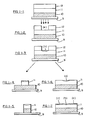
- Figures 1-1 through 2-8 are process flow diagrams showing cross-sectional views of the subsequent stages in the formation of a plasma etch-resistant mask on a polymer substrate or surface using the method in accordance with this invention.
- a substrate 10 such as a silicon wafer is coated with a passivation or dielectric polymer layer 11 which contains free carboxyl groups, and this layer is further overcoated with a resist material 12.
- the structure is next contacted with an aqueous solution containing cations under slightly acidic conditions which cations are incorporated into the surface of the polymer layer via diffusion and ion exchange to form a polymer salt in region (b) as shown in Figure 1-3.
- the structure is subjected to an RIE plasma etch treatment which etches away the remaining resist and the unmasked regions of polymer while leaving behind the masked polymer relief structure as shown in Figure 1-4.
- the substrate 10 may be essentially any material commonly employed in the fabrication of electrical and semiconductor devices. Suitable substrates include metals such as aluminum, chromium, copper or silver; silicon materials such as silicon dioxide, silicon nitride, phosphorous doped silicon dioxide and polycrystalline silicon; and polymeric materials such as dielectric polyimides or polyepoxides.
- Polymeric materials which comprise passivation or dielectric layer 11 include those polymers having superior thermal and insulating properties and also containing free carboxyl groups capable of complexing with selected cations.
- Such polymers include epoxy resins, and polyamides, as well as polyimides and polyesters each containing free carboxyl groups.
- polyamic acid polymers which are based on the condensation of aromatic dianhydrides with diamines, more preferably aromatic diamines.
- Suitable aromatic dianhydrides include pyromelittic dianhydride, 2,2-bis(3,4-dicarboxyphenyl) propane dianhydride, 2,3,6,7-naphthalene tetracarboxylic dianhydride, 2,2′,3,3′-diphenyl tetracarboxylic dianhydride, benzophenone tetracarboxylic dianhydride, and fluorinated materials such as 2,2-hexafluoro-bis (3,4-dicarboxyphenyl) propane dianhydride.
- Suitable diamines include m-phenylene diamine, p-phenylene diamine, 4,4′-diaminodiphenyl ether as well as fluorinated diamines such as 2,2-hexafluoro-bis (4-aminophenyl) propane.
- the polyamic acids may be partially imidized such as by heat or chemical cyclization as a method for controlling the number of free acid groups present in the polymer molecule, but not to the extent that an unsuitable number of free carboxyl groups remain available to complex with the metal ions contacted therewith.
- Suitable polyamic acids useful for the purposes of this invention generally have glass transition temperatures (Tg) in excess of 200 o C and their methods of preparation are disclosed in U.S. Patents 3,179,614, 3,264,250 and 3,310,573,the disclosure of which references is incorporated herein by reference.
- Particularly preferred polyamic acid polymers are available from the DuPont Company under the trade designation RC-5878 and PI 5057.
- Polyamic acid layer 11 may be formed in any conventional fashion. Typically it is applied by spin coating a solution of the polymer dissolved in a suitable inert solvent such as N-methylpyrrolidone and dried. The layer may be partially cured by heating at temperatures in the order of 100 to 200°C for about 5 to 20 minutes. Thicknesses of the dried layer are not limited, but typically will be in the order of from about 0.2 to about 10 microns.
- Resist layer 12 may be standard resist materials known in the art and may be positive acting or negative acting.
- the resists may be sensitive to near, mid and deep UV, electron beam, x-ray, ion beam or laser.
- Examples of such resists include novolak based resists containing light sensitive diazoquinone compounds such as disclosed in U.S. Patent 4,550,069 or the so called blocked resists based on copolymers containing blocked imide groups and a latent photoacid, such as disclosed in U.S. Patent 4,810,613.
- negative resists which contain photosensitive crosslinking agents or photopolymers such as disclosed in U.S. Patent 3,469,982 and Re 30,186. The resist selected must however be removable by conventional reactive ion etching processes.
- the resist layer 12 may be applied by any suitable process such as spin coating from solution followed by drying.
- the thickness of the dried resist may generally be of the same magnitude as the thickness of the polyamic acid layer, i.e. from about 0.2 to about 10 microns.
- Image patters are formed on the surface of polyamic acid layer 11 by exposing resist layer 12 through a mask followed by the usual development to remove the exposed or unexposed areas of the resist, depending on resist chemistry.
- the development step exposes that portion of the polyamic acid layer surface to be complexed with cations in accordance with this invention, while the remaining portions of the surface continue to be masked by the resist as illustrated in Figure 1-2.
- Positive resist materials are preferred for this invention since they may be developed using aqueous alkaline developer materials.
- Preferred developers comprise aqueous solutions of calcium hydroxide or tetramethyl ammonium hydroxide.
- the next stage of the process involves contacting the patterned surface prepared as above with an aqueous solution containing alkaline earth, transition metal or heavy metal cations in order that these cations may complex to form polyamate salts by diffusion and ion exchange with the free acid groups present in polymer layer 11, the patterned surface of which is exposed at interconnect zone (a) shown in Figure 1-2.
- Free cations may be generated in aqueous solutions of metallic salts or oxides, such as nitrates, halides, oxides, sulfates and the like as well as mixtures thereof.
- Suitable metal ions include alkaline earth metals of Group II A of the Periodic Table such as calcium, magnesium, barium, and strontium; heavy metals such as lead, cobalt and zinc; Group 1B metals such as copper and silver; and transition metals such as nickel, titanium, chromium and manganese.
- Ionically impure tap water may also be employed as the source of cations, generally yielding a mixed calcium/magnesium salt.
- any cation which is capable of complexing with the polyamic acid and will form salts or oxides when the complexed polyamic acid surface is subjected to an RIE etch treatment are operable for the purposes of this invention.
- the aqueous ionic solution may be prepared by dissolving the metallic compound in water to form a dilute solution.
- the cationic concentration in the solution is generally not critical, but 0.01 to 0.2 molar solutions are preferred. The lower the cationic concentration, the longer the time required for the cations to complex with the polyamic acid.
- the pH of the solution should be adjusted to fall in a range of from at least about 3.5 up to about 7.0.
- the cations are not effectively absorbed into the surface of the polyamic acid film layer and the polymer acid groups remain substantially unneutralized; at a higher pH of greater than about 7.0, the ionic solution tends to dissolve the polyamic acid layer.
- the pH adjustment may be accomplished by adding appropriate amounts of an acid to the aqueous solution, the preferred acids being weak acids such as acetic or phosphoric acid.
- the polyamic acid/ion salt complexes may be formed by simply contacting the exposed surface of polyamic acid layer 11 shown in Figure 1-2 with the aqueous cationic solution at room temperature. Contact may be accomplished by simple application of the solution to the surface by spraying, or pouring, or by immersion of the structure into the solution. Generally, the ion exchange and diffusion reaction will take place in a very short period of time, generally from about 30 seconds to about 5 minutes of contact time. After the reaction is complete, the structure is washed and dried to yield the modified barrier surface region shown as (b) in Figure 1-3.
- a particular advantage of the process of this invention is that it also provides a method for patterning conductive metallic layers on the surface of polyamic acid substrates. For example, cations of highly conductive metals such as silver may be diffused onto selective portions of the polyamic acid layer to form a silver rich polyamate surface, which when reduced by heating to about 350 o C, forms a conductive silver rich line pattern on the surface.
- etching may be accomplished using a wide variety of etching gases, the main criteria of such gases being that they are capable of etching away the non-masked areas of the relief structure while leaving the masked area behind as shown in Figure 1-4, and be reactive with the cation polyamate salt present in the selected portions of the polyamic acid layer to form cationic salts or oxides which are resistant to etching.
- the step of subjecting the substrate to gaseous plasma etch results in the in-situ formation of an etching mask as a consequence of the reaction between the gas and the cation rich polyamate salt.
- Etching may be carried out in a reactive ion etch reactor using standard wattage such as from about 100 to about 1,000 watts, standard gas flow rates and standard pressures, as are known in the prior art.
- Etching gases which may be employed include oxygen and mixtures of oxygen with inert gases such as argon or nitrogen. Gases based on halogen and halogen-containing compounds may also be employed, alone or in admixture with oxygen or an inert gas.
- Preferred halogen containing compounds generally contain not more the 2 carbon atoms and include CX4, C2X6,CFCl3, CF3CL, SX6, CCL2F2 and NX3, wherein X is halogen, preferably chlorine or fluorine.
- gases which may be used include nitrous oxide, carbon dioxide and carbon monoxide.
- the process of this invention essentially permits the selection of any etchant reactive with the polyamate cations to produce salts, such as halogen salts, or to produce metal oxides, all of which are significantly more resistant to etching than the photoresist and unmodified polyamic acid layers.
- some cation species may be non-reactive with some species of etching gas such that some routine experimentation by one skilled in the art may be required to match the proper etch gas to the appropriate cation species to produce the barrier salts or oxides.
- test data shows that calcium ions do not sufficiently react with oxygen gas under etching conditions to provide appropriate barrier properties, whereas calcium is sufficiently reactive with halogen-containing gases to produce such properties.
- a positive-acting photoresist composition based on a solution of a novolak resin and a diazoquinone sensitizer (AZ-1350J, available from Hoechst Celanese Corporation) was spun coated over the dried polyamic acid film and the structure was baked at 90 o C for 2 minutes.
- the resist layer was then exposed through a line mask to a mercury gas lamp under standard conditions for a time sufficient to photochemically alter that portion of the resist film exposed to the light. Exposure was followed by contact with an aqueous 5% by weight tetramethylamnonium hydroxide solution for about 50 seconds to develop the positive image in the resist layer only. The wafer was then dipped in a 0.5% aqueous solution of acetic acid for 2-3 minutes to neutralize any residual base. The cross sectional configuration of the structure at this stage is as depicted in Figure 1-2.
- the patterned wafer was then dipped in a 0.1M aqueous solution of copper nitrate (pH about 5) for 2 minutes, after which it was briefly rinsed with deionized tap water and dried. At this point the structure has the cross sectional configuration depicted in Figure 1-3, the surface region (b) being copper polyamate.
- Example 1 was repeated exactly as set forth, except in this example the ion exchange cation solution employed was a 0.1M aqueous lead nitrate solution instead of copper nitrate.
- Example 1 was repeated exactly as set forth, except in this example the ion exchange cation solution employed was a 0.1M aqueous solution of silver nitrate instead of copper nitrate.
- Example 1 was repeated exactly as set forth, except in this example the ion exchange cation solution employed was a 0.1M aqueous solution of calcium nitrate instead of copper nitrate.
- Etching conditions were: gas flow: 100 SCCM (Standard Cubic Centimeters per Minute); pressure: 6.67 N/m2 (50 millitors); power: 500 watts.
- Etching time for all samples was to endpoint plus 20% with respect to the control.
- Results are shown in Table 1.
- the number in the first column indicates the thickness of the masked cation polyamate layer (the region of polyamic acid under (b) as shown in Figure 1-3) prior to etching and the number in the second column (END) indicates the thickness of the same layer after etching to endpoint + 20%.
- the amount and percent of this layer etched is also shown, as well as the etch ratio which represents the degree of etching of the unmasked surface of the wafer with respect to the masked surface of the wafer.
- the data demonstrates the effective etch resistant properties imparted to the cation rich polyamate layer as a consequence of the reaction of the copper, lead and silver polyamate surface with the oxygen gas etchant. This is contrasted with the control and the calcium polyamate treatment which is not sufficiently reactive with oxygen to impart effective etch resistance.
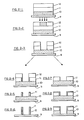
- FIGs 1-5 and 1-6 Yet another embodiment of the present invention is illustrated in Figures 1-5 and 1-6.
- the wafer structure is exposed, developed and treated with the ion exchange cation solution as set forth in Example 1 and as illustrated in Figures 1-1, 1-2, and 1-3.
- the next step in this embodiment is to strip away the remaining portion of resist layer 12 to expose the remaining surface of polyamic acid layer as shown in Figure 1-5.
- This stripping may be accomplished by soaking the wafer in a material which will dissolve resist layer 12 but leave the underlying polyamic acid layer essentially intact, such as by soaking in N-butylacetate for 2 to 3 minutes.
- etching gas which is reactive with only polyamate layer (b) or polyamate layer (c) and etching in the normal fashion
- positive or negative relief structures may be obtained.
- a negative relief structure similar to that depicted in Figure 1-4 may be obtained where the polyamate salt comprising regions (c) in Figure 1-6 is the calcium salt or another salt non-reactive with oxygen and the polyamate salt comprising region (b) in Figure 1-6 is copper, nickel, silver, or another species which is reactive with oxygen and provides RIE barrier properties as described herein.
- a positive relief structure analogous to that depicted in Figure 2-6 may be obtained by simply reversing the ion species contacted with polyamate layer 11, i.e., by using calcium ions or some other species which is not reactive with the oxygen etch to form the metal polyamate salt in region (b) of Figure 1-6, and using a different metal ion reactive with the oxygen etch to form the metal polyamate salt in regions (c) of Fig. 1-6.
- positive or negative relief structures may be made as a function of both the particular etch gas employed and the identity of the salt forming metal cation used to create polyamate regions (b) and (c).
- FIG. 2-1 may be of the same composition as that shown in Figure 1-1 except that an additional underlying substrate layer 9 may be provided.
- This layer may be composed of the same or similar material as layer 10 or may be composed of a different material such as metal or an insulating dielectric polymer such as a cured epoxy resin or a cured polyimide resin.
- Resist layer 12 is then exposed to radiation through a mask to provide the exposed region indicated by the shaded area of layer 12 in Figure 2-2.
- the structure is then developed using a developer which not only removes the exposed portion of resist layer 12 but also removes the portion of the polyamic acid layer underlying the exposed resist layer as depicted in Figure 2-3. Removal of both layers may be accomplished by treatment with an aqueous base such as tetramethyl-ammonium hydroxide as set forth in example 1, except that the contact time of the structure with the developer solution is longer, e.g., 2 minutes instead of 50 seconds.
- an aqueous base such as tetramethyl-ammonium hydroxide as set forth in example 1, except that the contact time of the structure with the developer solution is longer, e.g., 2 minutes instead of 50 seconds.
- the structure of Figure 2-3 may then be contacted with the aqueous cation solution as set forth above which will give rise to a structure wherein only side wall diffusion and ion exchange takes place. This is illustrated by the shaded areas in layer 11 shown in Figure 2-4. Reactive ion etching of this structure then gives rise to a relief structure composed of very thin durable pillars which are suitable for micro imaging as shown in Figure 2-5.
- positive relief structures may be obtained as depicted in Figures 2-1, 2-2, 2-3, 2-6, 2-7, and 2-8.
- a relief structure is prepared as set forth above and as depicted in Figure 2-3.
- Resist layer 12 is next stripped away such as by soaking the structure in N-butylacetate for 2 to 3 minutes as set forth above, leaving exposed the surfaces of polyamic acid layer 11 as shown in Figure 2-7.
- the structure is then contacted with the aqueous solution of cations causing the polyamate barrier salt to form on both the inner and top portions of polyamic acid layer 11 as shown by the shaded areas of Figure 2-8.
- the structure is then subjected to reactive ion etching under conditions sufficient to remove the exposed portions of substrate 10 while leaving both the masked area of polyamic acid layer 11 and underlying substrate 9 substantially intact.
- a positive relief structure as shown in Figure 2-9 results.
Landscapes
- Engineering & Computer Science (AREA)
- Physics & Mathematics (AREA)
- General Physics & Mathematics (AREA)
- Condensed Matter Physics & Semiconductors (AREA)
- Computer Hardware Design (AREA)
- Chemical & Material Sciences (AREA)
- Chemical Kinetics & Catalysis (AREA)
- General Chemical & Material Sciences (AREA)
- Architecture (AREA)
- Manufacturing & Machinery (AREA)
- Structural Engineering (AREA)
- Microelectronics & Electronic Packaging (AREA)
- Power Engineering (AREA)
- Photosensitive Polymer And Photoresist Processing (AREA)
- Drying Of Semiconductors (AREA)
- Exposure Of Semiconductors, Excluding Electron Or Ion Beam Exposure (AREA)
- Internal Circuitry In Semiconductor Integrated Circuit Devices (AREA)
Applications Claiming Priority (2)
| Application Number | Priority Date | Filing Date | Title |
|---|---|---|---|
| US421219 | 1989-10-13 | ||
| US07/421,219 US4968552A (en) | 1989-10-13 | 1989-10-13 | Versatile reactive ion etch barriers from polyamic acid salts |
Publications (3)
| Publication Number | Publication Date |
|---|---|
| EP0422375A2 true EP0422375A2 (de) | 1991-04-17 |
| EP0422375A3 EP0422375A3 (en) | 1991-10-16 |
| EP0422375B1 EP0422375B1 (de) | 1995-11-29 |
Family
ID=23669655
Family Applications (1)
| Application Number | Title | Priority Date | Filing Date |
|---|---|---|---|
| EP90116541A Expired - Lifetime EP0422375B1 (de) | 1989-10-13 | 1990-08-29 | Allgemeine Ätz-Stoppschichten aus Salzen von polyamischer Säure für reaktives ionisches Ätzen |
Country Status (4)
| Country | Link |
|---|---|
| US (1) | US4968552A (de) |
| EP (1) | EP0422375B1 (de) |
| JP (1) | JPH0793294B2 (de) |
| DE (1) | DE69023874T2 (de) |
Families Citing this family (13)
| Publication number | Priority date | Publication date | Assignee | Title |
|---|---|---|---|---|
| US5032216A (en) * | 1989-10-20 | 1991-07-16 | E. I. Du Pont De Nemours And Company | Non-photographic method for patterning organic polymer films |
| US5290397A (en) * | 1992-08-21 | 1994-03-01 | Cornell Research Foundation, Inc. | Bilayer resist and process for preparing same |
| US5912187A (en) * | 1993-12-30 | 1999-06-15 | Lucent Technologies Inc. | Method of fabricating circuits |
| TW309654B (de) * | 1995-03-29 | 1997-07-01 | Olin Corp | |
| US5660957A (en) * | 1996-05-16 | 1997-08-26 | Fujitsu Limited | Electron-beam treatment procedure for patterned mask layers |
| US5972145A (en) * | 1996-06-07 | 1999-10-26 | International Business Machines Corporation | Removable passivating polyimide coating and methods of use |
| US6022485A (en) * | 1997-10-17 | 2000-02-08 | International Business Machines Corporation | Method for controlled removal of material from a solid surface |
| KR20010042419A (ko) | 1998-04-02 | 2001-05-25 | 조셉 제이. 스위니 | 낮은 k 유전체를 에칭하는 방법 |
| US6124167A (en) * | 1999-08-06 | 2000-09-26 | Micron Technology, Inc. | Method for forming an etch mask during the manufacture of a semiconductor device |
| PH12001000675B1 (en) * | 2000-04-04 | 2009-09-22 | Australian Food Ind Sci Ct | Encapsulation of food ingredients |
| US20050119390A1 (en) * | 2003-12-02 | 2005-06-02 | Usa As Represented By The Administrator Of The National Aeronautics And Space Administration | Process for the simultaneous formation of surface and sub-surface metallic layers in polymer films |
| US7758927B2 (en) * | 2004-04-19 | 2010-07-20 | The United States Of America As Represented By The Administrator Of The National Aeronautics And Space Administration | Laser-induced fabrication of metallic interlayers and patterns in polyimide films |
| JPWO2005121019A1 (ja) * | 2004-06-08 | 2008-04-10 | 独立行政法人理化学研究所 | ナノ構造体の製造方法およびナノ構造体 |
Citations (3)
| Publication number | Priority date | Publication date | Assignee | Title |
|---|---|---|---|---|
| JPS58132927A (ja) * | 1982-02-03 | 1983-08-08 | Matsushita Electronics Corp | パタ−ン形成方法 |
| EP0249769A2 (de) * | 1986-06-10 | 1987-12-23 | International Business Machines Corporation | Strukturiertes Bild und Herstellungsverfahren desselben |
| EP0261315A1 (de) * | 1986-08-25 | 1988-03-30 | International Business Machines Corporation | Verfahren zum Erhöhen der Beständigkeit von Lackbildern gegen reaktive Ionenätzung und Wärmefluss |
Family Cites Families (10)
| Publication number | Priority date | Publication date | Assignee | Title |
|---|---|---|---|---|
| US4092209A (en) * | 1976-12-30 | 1978-05-30 | Rca Corp. | Silicon implanted and bombarded with phosphorus ions |
| JPS5656636A (en) * | 1979-10-13 | 1981-05-18 | Mitsubishi Electric Corp | Processing method of fine pattern |
| JPS58154859A (ja) * | 1982-03-11 | 1983-09-14 | Fuji Xerox Co Ltd | 複写機 |
| GB2121197A (en) * | 1982-05-26 | 1983-12-14 | Philips Electronic Associated | Plasma-etch resistant mask formation |
| US4430153A (en) * | 1983-06-30 | 1984-02-07 | International Business Machines Corporation | Method of forming an RIE etch barrier by in situ conversion of a silicon containing alkyl polyamide/polyimide |
| US4613398A (en) * | 1985-06-06 | 1986-09-23 | International Business Machines Corporation | Formation of etch-resistant resists through preferential permeation |
| US4751170A (en) * | 1985-07-26 | 1988-06-14 | Nippon Telegraph And Telephone Corporation | Silylation method onto surface of polymer membrane and pattern formation process by the utilization of silylation method |
| US4692205A (en) * | 1986-01-31 | 1987-09-08 | International Business Machines Corporation | Silicon-containing polyimides as oxygen etch stop and dual dielectric coatings |
| EP0238690B1 (de) * | 1986-03-27 | 1991-11-06 | International Business Machines Corporation | Verfahren zur Herstellung von Seitenstrukturen |
| JPS63136631A (ja) * | 1986-11-28 | 1988-06-08 | Sony Corp | パタ−ン形成方法 |
-
1989
- 1989-10-13 US US07/421,219 patent/US4968552A/en not_active Expired - Fee Related
-
1990
- 1990-08-29 DE DE69023874T patent/DE69023874T2/de not_active Expired - Fee Related
- 1990-08-29 EP EP90116541A patent/EP0422375B1/de not_active Expired - Lifetime
- 1990-09-07 JP JP2236021A patent/JPH0793294B2/ja not_active Expired - Lifetime
Patent Citations (3)
| Publication number | Priority date | Publication date | Assignee | Title |
|---|---|---|---|---|
| JPS58132927A (ja) * | 1982-02-03 | 1983-08-08 | Matsushita Electronics Corp | パタ−ン形成方法 |
| EP0249769A2 (de) * | 1986-06-10 | 1987-12-23 | International Business Machines Corporation | Strukturiertes Bild und Herstellungsverfahren desselben |
| EP0261315A1 (de) * | 1986-08-25 | 1988-03-30 | International Business Machines Corporation | Verfahren zum Erhöhen der Beständigkeit von Lackbildern gegen reaktive Ionenätzung und Wärmefluss |
Non-Patent Citations (5)
| Title |
|---|
| IBM TECHNICAL DISCLOSURE BULLETIN, vol. 27, no. 5, October 1984, page 3050, New York, US; L.C. LEE et al.: "Enhancement of terpolymer resist R/Ro through resist film surface treatment" * |
| JOURNAL OF POLYMER SCIENCE: PART B: POLYMER PHYSICS, vol. 26, 1989, pages 1485-1497; H.G. LINDE et al.: "Cation interactions with polyamic acids" * |
| JOURNAL OF VACUUM SCIENCE & TECHNOLOGY - Part B, vol. 5, no. 1, January-February 1987, pages 382-385, American Vacuum Society, Woodbury, N.Y, US; J.O. Choi et al.: "Enhanced plasma etch resistance of acrylic acid-calcium acetate modified poly(methylmethacrylate) * |
| JOURNAL OF VACUUM SCIENCE & TECHNOLOGY - PART B, vol. 5, no. 1. January- February 1987, pages 382-385; J.O. CHOI et al.: "Enhanced plasma etch resistance of acrylic acid-calcium acetate modified poly(methylmethacrylate)" * |
| PATENT ABSTRACTS OF JAPAN, vol. 7, no. 243 (E-207)[1388], 28th October 1983; & JP-A-58 132 927 (MATSUSHITA) 08-08-1983 * |
Also Published As
| Publication number | Publication date |
|---|---|
| EP0422375B1 (de) | 1995-11-29 |
| DE69023874D1 (de) | 1996-01-11 |
| EP0422375A3 (en) | 1991-10-16 |
| JPH0793294B2 (ja) | 1995-10-09 |
| US4968552A (en) | 1990-11-06 |
| JPH03138924A (ja) | 1991-06-13 |
| DE69023874T2 (de) | 1996-06-20 |
Similar Documents
| Publication | Publication Date | Title |
|---|---|---|
| EP0397988B1 (de) | Plasmabehandlung mit Metallmasken-Integration | |
| EP0230615A2 (de) | Polyimide mit Silizium, verwendet als Stop für das Sauerstoff-Ätzen und als zusammengesetzte dielektrische Beschichtungen | |
| EP0422375B1 (de) | Allgemeine Ätz-Stoppschichten aus Salzen von polyamischer Säure für reaktives ionisches Ätzen | |
| JPS6350860B2 (de) | ||
| JPH06326222A (ja) | 光学的画像形成可能材料、フォトレジスト材料等に高い高アスペクト比のvia及び溝を形成する方法 | |
| US4321317A (en) | High resolution lithography system for microelectronic fabrication | |
| JPH08250400A (ja) | シリコーン樹脂の除去法 | |
| JPH0368904B2 (de) | ||
| JPS61218133A (ja) | 半導体デバイスのパタ−ン形成方法 | |
| EP0349411A2 (de) | Gegen Sauerstoffplasma widerstandsfähige Photolacke | |
| US4289573A (en) | Process for forming microcircuits | |
| JPH08316121A (ja) | レジストパターン形成方法 | |
| US5114827A (en) | Photoresists resistant to oxygen plasmas | |
| US5213917A (en) | Plasma processing with metal mask integration | |
| US6221567B1 (en) | Method of patterning polyamic acid layers | |
| KR100392081B1 (ko) | 패턴형성방법 | |
| EP0077056B1 (de) | Gegen ionisierende Strahlung empfindlicher, negativ arbeitender Resist | |
| EP0200477A2 (de) | Bilderzeugungsverfahren | |
| JPH02156244A (ja) | パターン形成方法 | |
| EP0042894B1 (de) | Verfahren zum Formen eines Mikroschaltkreises | |
| JPS6256947A (ja) | 二層構造レジスト用平坦化層組成物 | |
| JPS62138843A (ja) | 複合レジスト構造体 | |
| JPH02135352A (ja) | 剥離液 | |
| KR100437614B1 (ko) | 반도체 소자의 금속 배선 형성 방법 | |
| JPH042183B2 (de) |
Legal Events
| Date | Code | Title | Description |
|---|---|---|---|
| PUAI | Public reference made under article 153(3) epc to a published international application that has entered the european phase |
Free format text: ORIGINAL CODE: 0009012 |
|
| 17P | Request for examination filed |
Effective date: 19901213 |
|
| AK | Designated contracting states |
Kind code of ref document: A2 Designated state(s): DE FR GB |
|
| PUAL | Search report despatched |
Free format text: ORIGINAL CODE: 0009013 |
|
| AK | Designated contracting states |
Kind code of ref document: A3 Designated state(s): DE FR GB |
|
| 17Q | First examination report despatched |
Effective date: 19931014 |
|
| GRAA | (expected) grant |
Free format text: ORIGINAL CODE: 0009210 |
|
| AK | Designated contracting states |
Kind code of ref document: B1 Designated state(s): DE FR GB |
|
| REF | Corresponds to: |
Ref document number: 69023874 Country of ref document: DE Date of ref document: 19960111 |
|
| ET | Fr: translation filed | ||
| PGFP | Annual fee paid to national office [announced via postgrant information from national office to epo] |
Ref country code: FR Payment date: 19960806 Year of fee payment: 7 |
|
| PG25 | Lapsed in a contracting state [announced via postgrant information from national office to epo] |
Ref country code: GB Effective date: 19960829 |
|
| PLBE | No opposition filed within time limit |
Free format text: ORIGINAL CODE: 0009261 |
|
| STAA | Information on the status of an ep patent application or granted ep patent |
Free format text: STATUS: NO OPPOSITION FILED WITHIN TIME LIMIT |
|
| 26N | No opposition filed | ||
| GBPC | Gb: european patent ceased through non-payment of renewal fee |
Effective date: 19960829 |
|
| PG25 | Lapsed in a contracting state [announced via postgrant information from national office to epo] |
Ref country code: DE Effective date: 19970501 |
|
| PG25 | Lapsed in a contracting state [announced via postgrant information from national office to epo] |
Ref country code: FR Free format text: LAPSE BECAUSE OF NON-PAYMENT OF DUE FEES Effective date: 19980430 |
|
| REG | Reference to a national code |
Ref country code: FR Ref legal event code: ST |