EP0416869A2 - Digital adder/accumulator - Google Patents
Digital adder/accumulator Download PDFInfo
- Publication number
- EP0416869A2 EP0416869A2 EP90309659A EP90309659A EP0416869A2 EP 0416869 A2 EP0416869 A2 EP 0416869A2 EP 90309659 A EP90309659 A EP 90309659A EP 90309659 A EP90309659 A EP 90309659A EP 0416869 A2 EP0416869 A2 EP 0416869A2
- Authority
- EP
- European Patent Office
- Prior art keywords
- carry
- bits
- bit
- adders
- circuit
- Prior art date
- Legal status (The legal status is an assumption and is not a legal conclusion. Google has not performed a legal analysis and makes no representation as to the accuracy of the status listed.)
- Granted
Links
Images


Classifications
-
- G—PHYSICS
- G06—COMPUTING; CALCULATING OR COUNTING
- G06F—ELECTRIC DIGITAL DATA PROCESSING
- G06F7/00—Methods or arrangements for processing data by operating upon the order or content of the data handled
- G06F7/38—Methods or arrangements for performing computations using exclusively denominational number representation, e.g. using binary, ternary, decimal representation
- G06F7/48—Methods or arrangements for performing computations using exclusively denominational number representation, e.g. using binary, ternary, decimal representation using non-contact-making devices, e.g. tube, solid state device; using unspecified devices
- G06F7/50—Adding; Subtracting
- G06F7/505—Adding; Subtracting in bit-parallel fashion, i.e. having a different digit-handling circuit for each denomination
- G06F7/506—Adding; Subtracting in bit-parallel fashion, i.e. having a different digit-handling circuit for each denomination with simultaneous carry generation for, or propagation over, two or more stages
-
- G—PHYSICS
- G06—COMPUTING; CALCULATING OR COUNTING
- G06F—ELECTRIC DIGITAL DATA PROCESSING
- G06F7/00—Methods or arrangements for processing data by operating upon the order or content of the data handled
- G06F7/38—Methods or arrangements for performing computations using exclusively denominational number representation, e.g. using binary, ternary, decimal representation
- G06F7/48—Methods or arrangements for performing computations using exclusively denominational number representation, e.g. using binary, ternary, decimal representation using non-contact-making devices, e.g. tube, solid state device; using unspecified devices
- G06F7/50—Adding; Subtracting
- G06F7/505—Adding; Subtracting in bit-parallel fashion, i.e. having a different digit-handling circuit for each denomination
- G06F7/509—Adding; Subtracting in bit-parallel fashion, i.e. having a different digit-handling circuit for each denomination for multiple operands, e.g. digital integrators
- G06F7/5095—Adding; Subtracting in bit-parallel fashion, i.e. having a different digit-handling circuit for each denomination for multiple operands, e.g. digital integrators word-serial, i.e. with an accumulator-register
Definitions
- the present invention generally relates to adding circuits and, more particularly, to an adding circuit for adding binary numbers and an accumulator for adding binary numbers sequentially supplied thereto in an accumulation fashion wherein high speed addition and accumulation can be executed without increasing the circuit scale thereof too much.
- the most popular adding circuit is formed of one half adder and (n - 1) all adders.
- this adding circuit is comprised of a half adder 1 and full adders 2.
- this popular adding circuit when carry data of the half adder of least significant bit (LSB) is gradually propagated to the full adders of most significant bit (MSB) to first provide accurate calculated results. Therefore, t assumes a calculation time of one full adder. Then, all calculation time T1 for adding binary number of n bits is expressed by the following equation (1): T1 ⁇ n t (1) Accordingly, if n is increased too much, a lot of calculation time is required depending on the calculation purpose.
- carry look ahead circuits 3A to 3D of 4 bits are connected in cascade to calculate beforehand only carry data at high speed.
- Adders 4A to 4D of 4 bits are provided to perform the addition assuming that carry data from less significant bits are "0”, whereas adders 5B to 5D of 4 bits are provided to perform the addition assuming that carry data from less significant bits are "1".
- Multiplexer circuits 6B to 6D are employed as switching circuits.
- the adder 4A adds 0'th to 3rd binary numbers (a3 ... a0 and b3 ... b0) of two binary numbers
- the adder 4B adds binary numbers of 4th to 7th bits (a7 ... a4 and b7 ... b4) assuming that carry data from less than 3 bits are "0”
- the adder 5B adds binary numbers of 4th to 7th bits assuming that the carry data from less than 3 bits are "1".
- the added result of binary numbers of 4th to 7th bits (c7 ... c4) can be obtained accurately.
- added results (c15 to c8) of 8th to 15th bits of the binary numbers can be obtained accurately, and a value c16 of 16th bit can be obtained as carry data of the carry look ahead circuit 3D of the most significant bit.
- a total calculation time required to perform the addition of binary numbers in the example of Fig. 2 becomes substantially equal to the calculation time of the 4-bit adder 4B or 5B.
- a circuit block 7D assumes a circuit formed of, for example, the adding circuits 4D and 5D and the multiplexer 6D. Then, an adding circuit which modifies the circuit block 7D is proposed as shown in Fig. 3.
- the technical report (Vol. 89, No. 4, PP. 37 to 44) of the Institute of Electronics, Informations and Communication Engineers describes this type of adding circuit.
- the 4-bit adding circuit 5D (see Fig. 2) for adding binary numbers is replaced with an adding circuit 8D for adding 1 to a binary number of 4 bits.
- This adding circuit 8D is interposed between the output port of the adder 4D and one input port of the multiplexer 6D.
- the calculation time at the adder 8D is added so that a total calculation time T3 is expressed as: T3 ⁇ kt (in the case of k ⁇ 2m) (3A) or T3 ⁇ 2mt (in the case of k ⁇ 2m) (3B)
- the circuit block of the example shown in Fig. 3 is employed, then the calculation speed is decreased to be substantially one half as compared with the original carry select adder type. In that case, however, the adding circuit 5D is replaced with the adding circuit 8D, which provides a reduced circuit scale. Even this circuit needs the multiplexers 6B to 6D, and there remains the substantial disadvantage that the circuit scale is very large.
- Fig. 4 shows an arrangement of a prior-art accumulator which accumulatively adds (i.e., accumulates) numbers x (x n-1 ... x1, x0) of less than n bits sequentially supplied thereto to obtain a sum s (s n-1 ...s1, s0) of n bits.
- an n-bit adder 201 is constructed by connecting a single 1-bit half adder 2020 and (n - 1) 1-bit full adders 2021 to 202 n-1 .
- Delay registers 2030 to 203 n-1 are shown to have clear terminals CLR and clock terminals CK. Sum outputs of the adders 2020 to 202 n-1 are respectively supplied to input terminals of the registers 2030 to 203 n-1 , data x0 to x n-1 of respective carries of numbers x are respectively supplied to one input terminals of the adders 2020 to 202 n-1 , and delayed outputs of the registers 2030 to 203 n-1 are supplied to the other input terminals of the adders 2020 to 202 n-1 , respectively.
- a reset signal R is supplied to the clear terminals CLR of the registers 2030 to 203 n-1 to reset the output data of these registers 2030 to 203 n-1 to zero.
- the number x supplied to the n-nit adder 201 is updated at a predetermined cycle and a clock pulse ⁇ 1 of this predetermined cycle is supplied to the clock terminals CK of the registers 2030 to 203 n-1 .
- the output of the n-bit adder 201 provides data S0 to S n-1 of respective carries of the sum s of n bits. In that case, the carry output from the n'th bit which is the most significant bit of the n-bit adder 201 to the (n + 1) bits can be neglected.
- n-bit adder 201 In the n-bit adder 201, however, the accurate sum output is not obtained until the carry output of the half adder 2020 propagates up to the full adder 202 n-1 . There is then the substantial disadvantage that, when the value n is increased, then the calculation speed is decreased. Assuming that T is the calculation time of the one 1-bit half adder or full adder, then a calculation time required by the accumulator of the example in Fig. 4 to perform one calculation is expressed as nearly nT.
- Japanese Patent Laid-Open Gazette No. 64-86271 describes another accumulator wherein regardless of the increase of the value n , a calculation time thereof is always substantially equal to the calculation time T of the single 1-bit full adder. This previously-proposed accumulator cannot avoid such a disadvantage that the circuit scale thereof still remains large. Further, it is frequently observed that the calculation speed is not always increased to the extent of the single 1-bit full adder.
- a digital adder circuit for adding binary numbers is comprised of a plurality of adders for adding the binary numbers divided at predetermined bits each, a carry calculator for calculating carry data to a higher bit of the predetermined bit on the basis of added results of the plurality of adders, and a carry corrector for adding the carry data to the added results of the plurality of adders within the predetermined bits.
- an accumulator for accumulating a plurality of binary numbers sequentially supplied thereto is comprised of more than two adders of a plurality of bits, a delay register for delaying each of outputs and each of carry outputs of the more than two adders of the plurality of bits by a predetermined time, the binary numbers sequentially supplied thereto and a delayed output of the delay register being sequentially added by the more than two adders of the plurality of bits, and a carry corrector supplied with an accumulated result expressed as redundant by each of outputs of the more than two adders of the plurality of bits and carry outputs and for correcting each of the outputs by each of the carry outputs to generate an accumulated added result having no redundancy.
- an adding circuit according to the present invention will be described with reference to Figs. 5 to 8.
- the present invention is applied to an adding circuit which obtains a binary number (c16, c15 ... c0) of 17 bits by adding two binary numbers (a15 ... a0) and (b15 ... b0) of 16 bits.
- Fig. 5 is a block diagram which shows the embodiment of the adding circuit according to the present invention.
- 4-bit adders 9A to 9D are provided to add two binary numbers of 4 bits.
- the binary numbers of 16 bits are divided to provide binary numbers of 4 bits each and binary numbers (a3 ... a0) and (b3 ... b0) of less significant 4 bits are added by the adder 9A.
- the binary numbers (a7 ... a4) and (b7 ... b4) of the next 4 bits are added by the adder 9B.
- the binary numbers (a11 ... a8) and (b11 ... b8) of the next 4 bits are added by the adder 9C.
- binary numbers (a15 ... a12) and (b15 ... b12) of the more significant 4 bits are added by the adder 9D.
- the carry data e4 of the adder 9A and the added results (d7 ... d4) of 4 bits from the adder 9B are supplied to input terminals of 5-input AND circuit 10B, and output data of this AND circuit 10B and the carry data e8 of the adder 9B are supplied to input terminals of an OR circuit 11b.
- Accurate carry data E8 to the 8th bit (which will be described later), which is the output data of the OR circuit 11B and added results (d11 ... d8) of 4 bits from the adder 9C are supplied to input terminals of a 5-input AND circuit 10C.
- Output data of this AND circuit 10C and carry data e12 of the adder 9C are supplied to an OR circuit 11C.
- adders 12B to 12D are provided to add binary numbers of 1 bit to binary numbers of 4 bits to obtain binary number of 4 bits. These adders 12B to 12D are referred hereinafter as "A4 blocks" in the following description. These A4 blocks 12B to 12D do not calculate carry data for 4th bit.
- the A4 block 12B adds the carry data e4 to the added results (d7 ... d4) of the adder 9B
- the A4 block 12C adds the accurate carry data E8 to the added results (d11 to d8)
- the A4 block 12D adds the accurate carry data E12 to the added results (d15 ... d12) of the adder 9D.
- the added results of 12 bits of these A4 blocks 12B to 12D are obtained as 12-bit values (c15 ... c4) of finally added results.
- Fig. 6 shows an example of the A4 block 12B (see Fig. 5).
- half adders 14A to 14D are provided, wherein an intermediate added result d4 and carry data e4 are supplied to different input terminals of the half adder 14A, respectively, intermediate added results d5 to d7 are supplied to one input terminals of the half adders 14B to 14D, respectively, and carry data from the half adders 14A, 14B and 14C are supplied to the other input terminals of the half adders 14B, 14C and 14D, respectively.
- the added results of these half adders 14A to 14D are obtained as final added results (c7 ... c4).
- a calculation time of one half adder is represented by t
- a total calculation time required by the A4 block 12B in the example of Fig. 6 to obtain an accurate value is substantially 4t.
- Fig. 7 shows another example of the A4 block 12B, in which reference numerals 15A to 15D designate exclusive-OR circuits, 16 a 2-input AND circuit, 17 a 3-input AND circuit and 18 a 4-input AND circuit, respectively.
- the intermediate added result d4 and carry data e4 are supplied to different input terminals of the exclusive-OR circuit 15A, different input terminals of the AND circuit 16, different input terminals of the AND circuit 17 and to different input terminals of the AND circuit 18.
- Output data of the AND circuit 16 is supplied to one input terminal of the exclusive-OR circuit 15B, while the intermediate added result d5 is supplied to the other input terminal of the exclusive-OR circuit 15B, a third input terminal of the AND circuit 17 and to a third input terminal of the AND circuit 18. Further, output data from the AND circuit 17 is supplied to one input terminal of the exclusive-OR circuit 15C, and the intermediate added result d6 is supplied to the other input terminal of the exclusive-OR circuit 15C and to a fourth input terminal of the AND circuit 18. Output data from the AND circuit 18 and the intermediate added result d7 are supplied to different input terminals of the exclusive-OR circuit 15D, respectively. Output data from these exclusive-OR circuits 15A to 15D are obtained as final added results (c7 to c4).
- Fig. 7 shows the circuit which performs the addition in a so-called table fashion. According to this circuit arrangement, the total calculation time can be reduced to about a calculation time of one all adder.
- Accurate carry data E12 to 12th bit is calculated (in step 107) from the carry data E8 and added result of 5 bits obtained in step 103, and accurate carry data E16 to 16th bit is obtained (in step 108) from the carry data E12 and added result of 5 bits obtained at step 104.
- step 101 less significant 4 bits of the added result in step 101 directly become less significant 4 bits (c3 ... c0) of added result finally obtained (in step 109).
- step 110 data of 4 bits (c7 ... c4) is obtained (in step 110) by adding the carry data e4 to the less significant 4 bits of the added result at step 102.
- Data of 4 bits (c11 ... c8) are obtained (in step 111) by adding the carry data E8 to less significant 4 bits of the added result in step 103, and data of 4 bits (c15 ... c12) are obtained (in step 112) by adding the carry data E12 to less significant 4 bits of the added result in step 104.
- the carry data E16 becomes data c16 which is finally provided as the most significant bit (MSB) (in step 113).
- T1 total calculation time
- this calculation time T x is slightly longer as compared with the total calculation time T2 (equation (2A) or (2B)) of the carry select adder system of the prior-art example shown in Fig. 2.
- the total calculation time T x is provided as a value which results from adding m t to the equation (4).
- the circuit scale of the example of Fig. 5 is made smaller than that of the carry select adder system because the circuit shown in Fig. 5 does not employ the multiplexer. Further, while the carry computers 13B, 13C and so on are supplied with only data of (m + 1) bits, the carry look ahead circuits 3A, 3B and the like in the example of Fig. 2 are supplied with data of (2m + 1) bits, the circuit scale of the carry computers 13B, 13c and the like can be reduced to substantially 1/2 as compared with that of the carry look ahead circuits 3A, 3B and the like. From this standpoint, there is then the advantage that the overall circuit scale can be made small.
- FIG. 9 A second embodiment of the present invention will be described with reference to Fig. 9.
- the present invention is applied to an adding circuit which produces a binary number of 10 bits (c9, c8 ... c0) by adding two binary numbers of 9 bits (a8 ... a0) and (b8 ... b0).
- input data of 9 bits are divided to provide 4 bits, 2 bits and 3 bits from the least significant bit (LSB).
- LSB least significant bit
- reference numeral 19 designates a 4-bit adder, 20 a 2-bit adder and a 21 a 3-bit adder, respectively.
- These adders 19, 20 and 21 perform the additions of binary numbers which are divided into 4 bits, 2 bits and 3 bits, respectively.
- Carry data e4 of the adder 19 and an added result of less significant 2 bits of the adder 20 are supplied to different input terminals of a 3-input AND circuit 22, respectively and output data of this 3-input AND circuit 22 and carry data e6 of the adder 20 are supplied to an OR circuit 24A, from which there is derived accurate carry data E6 to the 6th bit.
- accurate carry data E9 to the 9th bit is calculated from the carry data E6, an added result of less significant 3 bits of the adder 21 and carry data e9 of the adder 21.
- reference numeral 25 designates an adder (A2 block) which adds data e4 of 1 bit to the binary numbers of 2 bits and reference numeral 26 designates an adder (A3 block) which adds data E6 of 1 bit to the binary numbers of 3 bits.
- An added result of less significant 4 bits of the adder 19 an added result of 2 bits of the A2 block 25 and an added result of 3 bits of the A3 block become final added results (c8 ... c0) and the carry data E9 directly becomes a value c9 of final 9th bit.
- the operation and effects of the example of Fig. 9 are the same as those of the example of Fig. 5 and therefore need not be described.
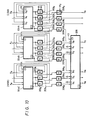
- FIG. 10 A first embodiment of an accumulator which utilizes the adding circuit of the present invention will be described with reference to Figs. 10 and 11.
- the present invention is applied to an accumulator circuit which produces a sum s (s8 ... S1, S0) of 9 bits by accumulating numbers x (x8 ... x1, x0) of less than 9 bits which are sequentially supplied thereto.
- Fig. 10 shows an accumulator of this embodiment.
- three 3-bit adders 204A to 204C are formed of three 1-bit full adders, delay registers 2030 to 2038 and 205A to 205B are provided, each of which has clear and clock terminals, and data holding registers 2060 to 2068 and 207A and 207B are provided, each of which has a clock terminal (each of these registers is represented by reference letter R in Fig. 10 for simplicity).
- a 6-bit adder 208 which is comprised of six 1-bit full adders.
- 0 is supplied to carry input terminal CI of the 3-bit adder 204A
- data x0 (LSB) to x2 of less significant 3 bits of the number x to be added are respectively supplied to one input terminals of the first bit input terminal b0 to the third bit input terminal b2 of the 3-bit adder 204A.
- Sum output of 3 bits therefrom are respectively supplied through the delay registers 2030 to 2032 to the other input terminals of the first bit input terminal b0 to the third bit input terminal b2 of the 3-bit adder 204A.
- a carry output to 4th bit produced at the carry output terminal CO of the delay register 204A is supplied through the delay register 205A to the carry input terminal CI of the 3-bit adder 204B.
- Data x3 to x5 of 3 bits of the number x to be added are respectively supplied to one input terminals of the first bit input terminal to the third input terminal of the 3-bit adder 204B, and sum outputs of 3 bits therefrom are respectively supplied through the delay registers 2033 to 2035 to the other input terminals of the first bit input terminal to the third bit input terminal.
- a carry output to 4th bit (7th bit as the numbers x) is supplied through the delay register 205B to the carry input terminal CI of the 3-bit adder 204C.
- data of more significant 3 bits x6 to x8 of the numbers x to be added are respectively supplied to one input terminals of the first to the third input terminals of the 3-bit adder 204C and sum outputs of 3 bits therefrom are respectively supplied through the delay registers 2036 to 2038 to the other input terminals of the first to third input terminals of the 3-bit adder 204C, while its carry output terminal CO being opened.
- Sum outputs of 3 bits from the 3-bit adder 204A are accumulated by the data holding registers 2060 to 2062 and provided as less significant 3 bits s0 to s2 of the sum s.
- a carry output of the 3-bit adder 204A is supplied through the data holding register 207A to one input terminal of the first bit b0 input terminal of the 6-bit adder 208 and 0 is supplied to the carry input terminal CI and one input terminals of the second bit b1 and third bit b2 input terminals of the 6-bit adder 208.
- the sum outputs of 3 bits from the 3-bit adder 204B are respectively supplied through the data holding registers 2063 to 2065 to the other input terminals of the first bit b0 to third bit b2 input terminals of the 6-bit adder 208.
- a carry output of the 3-bit adder 204B is supplied through the data holding register 207B to one input terminal of the fourth bit b3 input terminal of the 6-bit adder 208, and 0 is supplied to one input terminals of the fifth bit b4 and sixth bit b5 input terminals of the 6-bit adder 208.
- Sum outputs of 3 bits from the 3-bit adder 204C are respectively supplied through the data holding registers 2066 to 2068 to the other input terminals of the fourth bit b3 to sixth bit b5 input terminals of the 6-bit adder 208, and a carry output terminal CO of the 6-bit adder 208 is opened. Sum outputs of 6 bits from the 6-bit adder 208 become more significant 6 bits S3 to S8 of the sum s which is the accumulated result.
- the numbers x1 to x n are sequentially supplied at a predetermined cycle and a cycle of a clock pulse ⁇ 1 supplied to the delay registers 2030 to 2038, 205A and 205B is made coincident with the former predetermined cycle.
- a clock pulse ⁇ 2 supplied to the data holding registers 2060 to 2068 and 207A and 207B occurs only when the sum s of the numbers x1 to x n is finally generated in the expression of ordinary 9 bits.
- 0 is set as delay outputs of the delay registers 2030 to 2038, 205A and 205B by a reset pulse R for initialization and the numbers x1 (x18 ... x10) added during the first cycle are supplied thereto.
- the resultant added results are the numbers x1 (Fig. 11A), whereby the numbers x1 are generated as the sum outputs of the 3-bit adders 204A to 204C and two carry outputs are both 0.
- the sum outputs and the carry outputs (i.e., accummulated results of the previous time) of the 3-bit adders 204A to 204C are respectively fed through the delay registers 2030 to 2038, 205A and 205B to the input sides of the 3-bit adders 204A to 204C and approximately and simultaneously numbers x2 (x28 ... x20) added during the second cycle are supplied to the input sides of the 3-bit adders 204A to 204C, whereby outputs (s28 ... s20), c23 and c26 are obtained as sum outputs of the 3-bit adders 204A to 204C, a carry output to the third bit and a carry output to the sixth bit.
- the expression of the accumulated result of the sum outputs (s28 ... s20) and the carry outputs c23 and c26 is what might be called a redundancy expression. Since the above-mentioned redundancy expression is employed in this embodiment, when the numbers of 9 bits are added, it is not necessary to await that the carry output propagates from the first bit to the ninth bit gradually. Then, the carry output c23 to the fourth bit and carry output c26 to the seventh bit are added altogether during the next third cycle. Accordingly, assuming that T represents the calculation time of the 1-bit full adder, then the calculation time required by the accumulator of this embodiment to add data of 9 bits is equal to calculation times 3T of the 3-bit adders 204A to 204C.
- the sum outputs (s28 ... s20) and the carry outputs c23 and c26 are fed through the delay registers 2030 to 2038 and 205A and 205B back to the input sides of the 3-bit adders 204A to 204C and simultaneously numbers x3 (xs38 ... x30) of the third cycle are supplied to the input sides of these 3-bit adders 204A to 204C, thereby generating sum outputs (s38 ... S30), a carry output c33 to the fourth bit and a carry output c36 to the seventh bit as shown in Fig. 11C.
- the addition of the less significant 3 bits is executed by outputting the less significant 3 bits (s n2 , s n1 , s n0 ) of the sum outputs (s n8 ... s n0 ) directly, whereas the addition of the more significant 6 bits is executed by the 6-bit adder 208.
- accumulator in the example of Fig. 10 is generalized as shown in Fig. 12, and this type of accumulator will be described with reference to Fig. 12.
- reference numerals 2090 to 209 p-1 designate r-bit adders (p and r are integers larger than 2)
- 2030 to 203 pr-1 , 205 to 205 p-2 designate delay registers
- 2060 to 206 pr-1 and 207 to 207 p-2 designate data holding registers
- 210 designates a pr-bit adder.
- the aforenoted respective circuits are connected similarly to those of the example of Fig. 10.
- sums s (s pr-1 ... s1, s0) of pr bits are obtained by accumulating numbers x (x pr-1 ... x1, x0) of less than pr bits.
- the sums s are expressed as redundant by the sum outputs of the r-bit adders 2090 to 209 p-1 and the carry outputs.
- the addition of the pr bits is executed at r bits each. If the accumulated result, for example, is obtained in the form of sums of (pr ⁇ 1) bits, any one of these r-bit adders 2090 to 209 p-1 may be replaced with an adder of (r ⁇ 1) bits.
Abstract
Description
- The present invention generally relates to adding circuits and, more particularly, to an adding circuit for adding binary numbers and an accumulator for adding binary numbers sequentially supplied thereto in an accumulation fashion wherein high speed addition and accumulation can be executed without increasing the circuit scale thereof too much.
- As an adding circuit for adding binary numbers (an-1, ... a₁, a₀) and (bn-1, ... b₁, b₀) of n bits (n is an integer larger than 2) to provide binary numbers (cn, ... c₁, c₀) of (n + 1) bits, the most popular adding circuit is formed of one half adder and (n - 1) all adders.
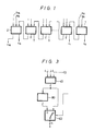
- Fig. 1 shows an example of such prior-art adding circuit, wherein n = 16.
- As shown in Fig. 1, this adding circuit is comprised of a
half adder 1 andfull adders 2. In this popular adding circuit, when carry data of the half adder of least significant bit (LSB) is gradually propagated to the full adders of most significant bit (MSB) to first provide accurate calculated results. Therefore, t assumes a calculation time of one full adder. Then, all calculation time T₁ for adding binary number of n bits is expressed by the following equation (1):
T₁ ≒ n t (1)
Accordingly, if n is increased too much, a lot of calculation time is required depending on the calculation purpose. - In order to realize the high speed addition, an adding circuit of carry select adder system is proposed. Fig. 2 shows an example of the previously-proposed carry select adder type adding circuit in which n = 16, by way of example.
- As shown in Fig. 2, carry look ahead
circuits 3A to 3D of 4 bits are connected in cascade to calculate beforehand only carry data at high speed.Adders 4A to 4D of 4 bits are provided to perform the addition assuming that carry data from less significant bits are "0", whereasadders 5B to 5D of 4 bits are provided to perform the addition assuming that carry data from less significant bits are "1".Multiplexer circuits 6B to 6D are employed as switching circuits. - The
adder 4A adds 0'th to 3rd binary numbers (a₃ ... a₀ and b₃ ... b₀) of two binary numbers, theadder 4B adds binary numbers of 4th to 7th bits (a₇ ... a₄ and b₇ ... b₄) assuming that carry data from less than 3 bits are "0", and theadder 5B adds binary numbers of 4th to 7th bits assuming that the carry data from less than 3 bits are "1". By selecting the added result of theadder multiplexer 6B in response to whether the carry data from the carry look aheadcircuit 3A is "0" or "1", the added result of binary numbers of 4th to 7th bits (c₇ ... c₄) can be obtained accurately. In the same fashion, added results (c₁₅ to c₈) of 8th to 15th bits of the binary numbers can be obtained accurately, and a value c₁₆ of 16th bit can be obtained as carry data of the carry look aheadcircuit 3D of the most significant bit. - Accordingly, a total calculation time required to perform the addition of binary numbers in the example of Fig. 2 becomes substantially equal to the calculation time of the 4-
bit adder circuit
T₂ ≒ kt (in the case of k ≧ m) (2A)
or T₂ ≒ mt (in the case of k < m) (2B)
It is to be appreciated from the foregoing equations (2A) and (2B) that, as compared with the case of the standard adding circuit (see equation (1)), this can perform the calculation at speed as high as m times to k times. - In the adding circuit of the carry select adder system, a
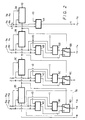
circuit block 7D assumes a circuit formed of, for example, the addingcircuits multiplexer 6D. Then, an adding circuit which modifies thecircuit block 7D is proposed as shown in Fig. 3. The technical report (Vol. 89, No. 4, PP. 37 to 44) of the Institute of Electronics, Informations and Communication Engineers describes this type of adding circuit. - Referring to Fig. 3, the 4-
bit adding circuit 5D (see Fig. 2) for adding binary numbers is replaced with an addingcircuit 8D for adding 1 to a binary number of 4 bits. This addingcircuit 8D is interposed between the output port of theadder 4D and one input port of themultiplexer 6D. In that case, the calculation time at theadder 8D is added so that a total calculation time T₃ is expressed as:
T₃ ≒ kt (in the case of k ≧ 2m) (3A)
or T₃ ≒ 2mt (in the case of k < 2m) (3B) - Although the calculation speed of the adding circuit of the carry select adder type can be increased as described above, this adding circuit needs the addition of the
multiplexers 6B to 6D, which unavoidably makes the circuit scale large. - Further, if the circuit block of the example shown in Fig. 3 is employed, then the calculation speed is decreased to be substantially one half as compared with the original carry select adder type. In that case, however, the adding
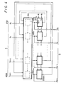
circuit 5D is replaced with the addingcircuit 8D, which provides a reduced circuit scale. Even this circuit needs themultiplexers 6B to 6D, and there remains the substantial disadvantage that the circuit scale is very large. - Fig. 4 shows an arrangement of a prior-art accumulator which accumulatively adds (i.e., accumulates) numbers x (xn-1 ... x₁, x₀) of less than n bits sequentially supplied thereto to obtain a sum s (sn-1...s₁, s₀) of n bits.
- With reference to Fig. 4, an n-
bit adder 201 is constructed by connecting a single 1-bit half adder 202₀ and (n - 1) 1-bitfull adders 202₁ to 202n-1.Delay registers 203₀ to 203n-1 are shown to have clear terminals CLR and clock terminals CK. Sum outputs of theadders 202₀ to 202n-1 are respectively supplied to input terminals of theregisters 203₀ to 203n-1, data x₀ to xn-1 of respective carries of numbers x are respectively supplied to one input terminals of theadders 202₀ to 202n-1, and delayed outputs of theregisters 203₀ to 203n-1 are supplied to the other input terminals of theadders 202₀ to 202n-1, respectively. - When the accumulative addition is carried out by the accumulator in the example of Fig. 4, a reset signal R is supplied to the clear terminals CLR of the
registers 203₀ to 203n-1 to reset the output data of theseregisters 203₀ to 203n-1 to zero. Then, the number x supplied to the n-nit adder 201 is updated at a predetermined cycle and a clock pulse ø1 of this predetermined cycle is supplied to the clock terminals CK of theregisters 203₀ to 203n-1. Thus, the output of the n-bit adder 201 provides data S₀ to Sn-1 of respective carries of the sum s of n bits. In that case, the carry output from the n'th bit which is the most significant bit of the n-bit adder 201 to the (n + 1) bits can be neglected. - In the n-
bit adder 201, however, the accurate sum output is not obtained until the carry output of thehalf adder 202₀ propagates up to the full adder 202n-1. There is then the substantial disadvantage that, when the value n is increased, then the calculation speed is decreased. Assuming that T is the calculation time of the one 1-bit half adder or full adder, then a calculation time required by the accumulator of the example in Fig. 4 to perform one calculation is expressed as nearly nT. - Japanese Patent Laid-Open Gazette No. 64-86271 describes another accumulator wherein regardless of the increase of the value n, a calculation time thereof is always substantially equal to the calculation time T of the single 1-bit full adder. This previously-proposed accumulator cannot avoid such a disadvantage that the circuit scale thereof still remains large. Further, it is frequently observed that the calculation speed is not always increased to the extent of the single 1-bit full adder.
- Accordingly, it is an object of the present invention to provide an improved adding circuit whose calculation speed is higher as compared with a conventional adding circuit.
- More specifically, it is an object of the present invention to provide an adding circuit which can make the calculation speed high and in which the circuit scale can be reduced as compared with a conventional carry select adder type adding circuit.
- It is another object of the present invention to provide an accumulator in which an accumulative addition can be performed at a necessary calculation speed dependent on the usage without increasing the circuit scale too much.
- As a first aspect of the present invention, a digital adder circuit for adding binary numbers is comprised of a plurality of adders for adding the binary numbers divided at predetermined bits each, a carry calculator for calculating carry data to a higher bit of the predetermined bit on the basis of added results of the plurality of adders, and a carry corrector for adding the carry data to the added results of the plurality of adders within the predetermined bits.
- In accordance with a second aspect of the present invention, an accumulator for accumulating a plurality of binary numbers sequentially supplied thereto is comprised of more than two adders of a plurality of bits, a delay register for delaying each of outputs and each of carry outputs of the more than two adders of the plurality of bits by a predetermined time, the binary numbers sequentially supplied thereto and a delayed output of the delay register being sequentially added by the more than two adders of the plurality of bits, and a carry corrector supplied with an accumulated result expressed as redundant by each of outputs of the more than two adders of the plurality of bits and carry outputs and for correcting each of the outputs by each of the carry outputs to generate an accumulated added result having no redundancy.
- The preceding, and other objects, features and advantages of the present invention will be apparent in the following detailed description of preferred embodiments when read in conjunction with the accompanying drawings, in which like reference numerals are used to identify the same or similar parts in the several views.
-
- Fig. is a schematic block diagram showing an example of a standard adding circuit of the prior art;
- Fig. 2 is a schematic block diagram showing a prior-art adding circuit of a carry select adder system;
- Fig. 3 is a schematic block diagram showing a modified example of the conventional carry select adder system adding circuit shown in Fig. 2;
- Fig. 4 is a schematic block diagram showing an example of a conventional accumulator;
- Fig. 5 is a block diagram showing a first embodiment of an adding circuit according to the present invention;
- Fig. 6 is a schematic block diagram showing a main portion of the adding circuit of Fig. 5;
- Fig. 7 is a schematic block diagram showing another example of the main portion of the adding circuit shown in Fig. 5;
- Fig. 8 is a schematic diagram used to explain an operation of the adding circuit of Fig. 5;
- Fig. 9 is a schematic block diagram showing a second embodiment of the adding circuit according to the present invention;
- Fig. 10 is a schematic block diagram showing an embodiment of the accumulator according to the present invention;
- Figs. 11A to 11E are schematic representations used to explain an operation of the embodiment shown in Fig. 10; and
- Fig. 12 is a schematic block diagram showing another embodiment of the accumulator which is provided by generalizing the accumulator of the present invention shown in Fig. 10.
- An embodiment of an adding circuit according to the present invention will be described with reference to Figs. 5 to 8. In this embodiment, the present invention is applied to an adding circuit which obtains a binary number (c₁₆, c₁₅ ... c₀) of 17 bits by adding two binary numbers (a₁₅ ... a₀) and (b₁₅ ... b₀) of 16 bits.
- Fig. 5 is a block diagram which shows the embodiment of the adding circuit according to the present invention.
- With reference to Fig. 5, 4-
bit adders 9A to 9D are provided to add two binary numbers of 4 bits. The binary numbers of 16 bits are divided to provide binary numbers of 4 bits each and binary numbers (a₃ ... a₀) and (b₃ ... b₀) of less significant 4 bits are added by theadder 9A. The binary numbers (a₇ ... a₄) and (b₇ ... b₄) of the next 4 bits are added by theadder 9B. The binary numbers (a₁₁ ... a₈) and (b₁₁ ... b₈) of the next 4 bits are added by theadder 9C. Finally, binary numbers (a₁₅ ... a₁₂) and (b₁₅ ... b₁₂) of the more significant 4 bits are added by theadder 9D. The added outputs of 4 bits excepting the carry data of theadder 9A is provided as the less significant 4 bits (c₃ ... c₀) of finally obtained added result, while carry data e₄, e₈, e₁₂, e₁₆ are generated from carry output terminals CA of theadders 9A to 9D, respectively. - The carry data e₄ of the
adder 9A and the added results (d₇ ... d₄) of 4 bits from theadder 9B are supplied to input terminals of 5-input ANDcircuit 10B, and output data of this ANDcircuit 10B and the carry data e₈ of theadder 9B are supplied to input terminals of an OR circuit 11b. Accurate carry data E₈ to the 8th bit (which will be described later), which is the output data of theOR circuit 11B and added results (d₁₁ ... d₈) of 4 bits from theadder 9C are supplied to input terminals of a 5-input ANDcircuit 10C. Output data of this ANDcircuit 10C and carry data e₁₂ of theadder 9C are supplied to an ORcircuit 11C. Accurate carry data E₁₂ to the 12th bit, which is the output data from theOR circuit 11C, and added results (d₁₅ ... d₁₂) of 4 bits from theadder 9D are supplied to input terminals of a 5-input ANDcircuit 10D, and output data from the ANDcircuit 10D and carry data e₁₆ of theadder 9D are supplied to input terminals ofOR circuit 11D. Output data E₁₆ of this ORcircuit 11D is provided as 16th bit value c₁₆ of final added result. Therefore, the circuit groups (10B, 11b), (10C, 11C) and (10D, 11D) can be regarded as carry computers (or calculators) 13B, 13C and 13D, respectively. - As illustrated in Fig. 5,
adders 12B to 12D are provided to add binary numbers of 1 bit to binary numbers of 4 bits to obtain binary number of 4 bits. Theseadders 12B to 12D are referred hereinafter as "A4 blocks" in the following description. These A4 blocks 12B to 12D do not calculate carry data for 4th bit. TheA4 block 12B adds the carry data e₄ to the added results (d₇ ... d₄) of theadder 9B, theA4 block 12C adds the accurate carry data E₈ to the added results (d₁₁ to d₈), and theA4 block 12D adds the accurate carry data E₁₂ to the added results (d₁₅ ... d₁₂) of theadder 9D. The added results of 12 bits of these A4 blocks 12B to 12D are obtained as 12-bit values (c₁₅ ... c₄) of finally added results. - Fig. 6 shows an example of the A4 block 12B (see Fig. 5).
- Referring to Fig. 6,
half adders 14A to 14D are provided, wherein an intermediate added result d₄ and carry data e₄ are supplied to different input terminals of thehalf adder 14A, respectively, intermediate added results d₅ to d₇ are supplied to one input terminals of thehalf adders 14B to 14D, respectively, and carry data from thehalf adders half adders half adders 14A to 14D are obtained as final added results (c₇ ... c₄). In that case, assuming that a calculation time of one half adder is represented by t, a total calculation time required by the A4 block 12B in the example of Fig. 6 to obtain an accurate value is substantially 4t. - Fig. 7 shows another example of the A4 block 12B, in which
reference numerals 15A to 15D designate exclusive-OR circuits, 16 a 2-input AND circuit, 17 a 3-input AND circuit and 18 a 4-input AND circuit, respectively. As shown in Fig. 7, the intermediate added result d₄ and carry data e₄ are supplied to different input terminals of the exclusive-OR circuit 15A, different input terminals of the ANDcircuit 16, different input terminals of the ANDcircuit 17 and to different input terminals of the AND circuit 18. Output data of the ANDcircuit 16 is supplied to one input terminal of the exclusive-OR circuit 15B, while the intermediate added result d₅ is supplied to the other input terminal of the exclusive-OR circuit 15B, a third input terminal of the ANDcircuit 17 and to a third input terminal of the AND circuit 18. Further, output data from the ANDcircuit 17 is supplied to one input terminal of the exclusive-OR circuit 15C, and the intermediate added result d₆ is supplied to the other input terminal of the exclusive-OR circuit 15C and to a fourth input terminal of the AND circuit 18. Output data from the AND circuit 18 and the intermediate added result d₇ are supplied to different input terminals of the exclusive-OR circuit 15D, respectively. Output data from these exclusive-OR circuits 15A to 15D are obtained as final added results (c₇ to c₄). - The addition in which binary numbers (d₇ ... d₄) of 4 bits can be added with the carry data e₄ of one bit in the example of Fig. 7 will be described in detail.
- Only when (d₄, e₄) = (1, 0) or (d₄, e₄) = (0, 1), the value c₄ becomes "1" so that the output data of the exclusive-
OR circuit 15A becomes the value C₄, accurately. Further, assuming that f₁ represents carry data from 0'th bit to 1st bit, then f₁ becomes "1" only when (d₄, e₄) = (1,1), while the value c₅ becomes "1" only when (d₅, f₁) = (1,0) or (d₅, f₁) = (0,1). Thus, the output data from the exclusive-OR circuit 15B takes the value c₅, accurately. Similarly, assuming that f₂ represents carry data to the 2nd bit and that f₃ represents carry data to the 3rd bit, then f₂ becomes "1" only when (d₅, d₄, e₄) = (1, 1, 1) and f₃ becomes "1" only when 1(d₆, d₅, d₄, e₄ = (1, 1, 1, 1). Therefore, the output data from the exclusive-OR circuits - The example of Fig. 7 shows the circuit which performs the addition in a so-called table fashion. According to this circuit arrangement, the total calculation time can be reduced to about a calculation time of one all adder.
- While in the above-mentioned example, the carry data to the 8th, 12th and 16th are not calculated in the respective A4 blocks 12B, 12C and 12D, these carry data are calculated by the carry computers (or calculator) 13B, 13C and 13D, respectively. A calculation in which accurate carry data E₈ to the 8th bit is obtained by the
carry computer 13B will be described first. - The carry data E₈ becomes "1" only when carry data e₈ of 4-
bit adder 9B is "1" or when carry data e₄ of the less significant 4-bit adder 9A and the added result (d₇ ... d₄) of theadder 9B suffice (d₇, d₆, d₅, d₄, e₄) = (1, 1, 1, 1, 1). Accordingly, thecarry computer 13B, formed by the combination of the 5-input ANDcircuit 10B and theOR circuit 11B, can derive accurate carry data E₈ to the 8th bit. - Further, the accurate carry data E₁₂ to the 12th bit becomes "1" only when carry data e₁₂ of the
adder 9C is "1" or when carry data E₈ to 8th bit and added result (d₁₁ ... d₈) of theadder 9C suffice (d₁₁, d₁₀, d₉, d₈, E₈ = (1, 1, 1, 1, 1). Therefore, accurate carry data E₁₂ to 12th bit can be obtained by the carry computer 13C which is formed by the combination of the 5-input ANDcircuit 10C and theOR circuit 11C. Similarly, accurate carry data E₁₆ to 16th bit can be obtained by thecarry computer 13D which is formed by the combination of the 5-input ANDcircuit 10D and theOR circuit 11D. - An operation in which two binary numbers can be added in the example of Fig. 5 will be summarized with reference to Fig. 8. Initially, two binary numbers are divided into 4 sections of 4 bits and additions are performed for these 4 sections of 4 bits in
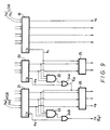
steps 101 to 104. Then, carry data e₄ obtained instep 101 directly becomes accurate carry data to 4th bit (at step 105), and accurate carry data E₈ to 8th bit is calculated (in step 106) from the carry data e₄ and added result of 5 bits obtained instep 102. Accurate carry data E₁₂ to 12th bit is calculated (in step 107) from the carry data E₈ and added result of 5 bits obtained instep 103, and accurate carry data E₁₆ to 16th bit is obtained (in step 108) from the carry data E₁₂ and added result of 5 bits obtained atstep 104. - Finally, less significant 4 bits of the added result in
step 101 directly become less significant 4 bits (c₃ ... c₀) of added result finally obtained (in step 109). Then, data of 4 bits (c₇ ... c₄) is obtained (in step 110) by adding the carry data e₄ to the less significant 4 bits of the added result atstep 102. Data of 4 bits (c₁₁ ... c₈) are obtained (in step 111) by adding the carry data E₈ to less significant 4 bits of the added result instep 103, and data of 4 bits (c₁₅ ... c₁₂) are obtained (in step 112) by adding the carry data E₁₂ to less significant 4 bits of the added result instep 104. The carry data E₁₆ becomes data c₁₆ which is finally provided as the most significant bit (MSB) (in step 113). - Let us now evaluate a total calculation time Tx of the example shown in Fig. 5, in which two input data assume binary numbers of n bits and the addition is performed under the condition that these input data are divided by m bits each. That is, n = km (k is an integer) is established and the
adders 9A to 9D are replaced with k m-bit adders. In that case, the calculation times of thecarry computers 13B, 13C and the like are approximately the same as the calculation time t of one 1-bit full adder so that, when the circuilt similar to that of the example of Fig. 7 is employed as the A4 blocks 12B, 12C or the like, the calculation times of the A4 blocks 12B, 12C or the like become substantially t. Thus, the total calculation time Tx is expressed as:
Tx ≒ {m + (k - 2) + 1} t = (m + k - 1) t (4)
Thus, the total calculation time Tx in this example can be considerably reduced as compared with the total calculation time T₁ (equation (1)) of the prior-art example shown in Fig. 1. However, this calculation time Tx is slightly longer as compared with the total calculation time T₂ (equation (2A) or (2B)) of the carry select adder system of the prior-art example shown in Fig. 2. - When the circuit in the example of Fig. 6 is employed as the A4 blocks 12B, 12C or the like, the total calculation time Tx is provided as a value which results from adding m t to the equation (4).
- The circuit scale of the example of Fig. 5 is made smaller than that of the carry select adder system because the circuit shown in Fig. 5 does not employ the multiplexer. Further, while the
carry computers 13B, 13C and so on are supplied with only data of (m + 1) bits, the carry look aheadcircuits carry computers 13B, 13c and the like can be reduced to substantially 1/2 as compared with that of the carry look aheadcircuits - A second embodiment of the present invention will be described with reference to Fig. 9. In this embodiment, the present invention is applied to an adding circuit which produces a binary number of 10 bits (c₉, c₈ ... c₀) by adding two binary numbers of 9 bits (a₈ ... a₀) and (b₈ ... b₀).
- In this embodiment, input data of 9 bits are divided to provide 4 bits, 2 bits and 3 bits from the least significant bit (LSB).
- In Fig. 9,
reference numeral 19 designates a 4-bit adder, 20 a 2-bit adder and a 21 a 3-bit adder, respectively. Theseadders adder 19 and an added result of less significant 2 bits of theadder 20 are supplied to different input terminals of a 3-input ANDcircuit 22, respectively and output data of this 3-input ANDcircuit 22 and carry data e₆ of theadder 20 are supplied to an ORcircuit 24A, from which there is derived accurate carry data E₆ to the 6th bit. Then, accurate carry data E₉ to the 9th bit is calculated from the carry data E₆, an added result of less significant 3 bits of theadder 21 and carry data e₉ of theadder 21. - Further, in Fig. 9,
reference numeral 25 designates an adder (A2 block) which adds data e₄ of 1 bit to the binary numbers of 2 bits andreference numeral 26 designates an adder (A3 block) which adds data E₆ of 1 bit to the binary numbers of 3 bits. An added result of less significant 4 bits of theadder 19, an added result of 2 bits of theA2 block 25 and an added result of 3 bits of the A3 block become final added results (c₈ ... c₀) and the carry data E₉ directly becomes a value c₉ of final 9th bit. The operation and effects of the example of Fig. 9 are the same as those of the example of Fig. 5 and therefore need not be described. - A first embodiment of an accumulator which utilizes the adding circuit of the present invention will be described with reference to Figs. 10 and 11. In this embodiment, the present invention is applied to an accumulator circuit which produces a sum s (s₈ ... S₁, S₀) of 9 bits by accumulating numbers x (x₈ ... x₁, x₀) of less than 9 bits which are sequentially supplied thereto.
- Fig. 10 shows an accumulator of this embodiment. Referring to Fig. 10, three 3-
bit adders 204A to 204C are formed of three 1-bit full adders, delay registers 203₀ to 203₈ and 205A to 205B are provided, each of which has clear and clock terminals, anddata holding registers 206₀ to 206₈ and 207A and 207B are provided, each of which has a clock terminal (each of these registers is represented by reference letter R in Fig. 10 for simplicity). Further, there is shown a 6-bit adder 208 which is comprised of six 1-bit full adders. - In this embodiment, 0 is supplied to carry input terminal CI of the 3-
bit adder 204A, and data x₀ (LSB) to x₂ of less significant 3 bits of the number x to be added are respectively supplied to one input terminals of the first bit input terminal b₀ to the third bit input terminal b₂ of the 3-bit adder 204A. Sum output of 3 bits therefrom are respectively supplied through the delay registers 203₀ to 203₂ to the other input terminals of the first bit input terminal b₀ to the third bit input terminal b₂ of the 3-bit adder 204A. A carry output to 4th bit produced at the carry output terminal CO of thedelay register 204A is supplied through thedelay register 205A to the carry input terminal CI of the 3-bit adder 204B. - Data x₃ to x₅ of 3 bits of the number x to be added are respectively supplied to one input terminals of the first bit input terminal to the third input terminal of the 3-
bit adder 204B, and sum outputs of 3 bits therefrom are respectively supplied through the delay registers 203₃ to 203₅ to the other input terminals of the first bit input terminal to the third bit input terminal. A carry output to 4th bit (7th bit as the numbers x) is supplied through thedelay register 205B to the carry input terminal CI of the 3-bit adder 204C. Simultaneously, data of more significant 3 bits x₆ to x₈ of the numbers x to be added are respectively supplied to one input terminals of the first to the third input terminals of the 3-bit adder 204C and sum outputs of 3 bits therefrom are respectively supplied through the delay registers 203₆ to 203₈ to the other input terminals of the first to third input terminals of the 3-bit adder 204C, while its carry output terminal CO being opened. - Sum outputs of 3 bits from the 3-
bit adder 204A are accumulated by thedata holding registers 206₀ to 206₂ and provided as less significant 3 bits s₀ to s₂ of the sum s. A carry output of the 3-bit adder 204A is supplied through thedata holding register 207A to one input terminal of the first bit b₀ input terminal of the 6-bit adder bit adder 208. The sum outputs of 3 bits from the 3-bit adder 204B are respectively supplied through thedata holding registers 206₃ to 206₅ to the other input terminals of the first bit b₀ to third bit b₂ input terminals of the 6-bit adder 208. A carry output of the 3-bit adder 204B is supplied through thedata holding register 207B to one input terminal of the fourth bit b₃ input terminal of the 6-bit adder bit adder 208. Sum outputs of 3 bits from the 3-bit adder 204C are respectively supplied through thedata holding registers 206₆ to 206₈ to the other input terminals of the fourth bit b₃ to sixth bit b₅ input terminals of the 6-bit adder 208, and a carry output terminal CO of the 6-bit adder 208 is opened. Sum outputs of 6 bits from the 6-bit adder 208 become more significant 6 bits S₃ to S₈ of the sum s which is the accumulated result. - An operation of this accumulator will be described with reference to Figs. 11A to 11E. In that case, the numbers x to be sequentially supplied are represented n numbers (n is an integer larger than 2) of x₁ to xn and the bit arrangement of the number xi (i = 1 to n) is expressed by (xn8 (MSB) to xn1, xn0 (LSB)). Further, the numbers x₁ to xn are sequentially supplied at a predetermined cycle and a cycle of a clock pulse ø₁ supplied to the delay registers 203₀ to 203₈, 205A and 205B is made coincident with the former predetermined cycle. Also, a clock pulse ø₂ supplied to the
data holding registers 206₀ to 206₈ and 207A and 207B occurs only when the sum s of the numbers x₁ to xn is finally generated in the expression of ordinary 9 bits. - In this embodiment, 0 is set as delay outputs of the delay registers 203₀ to 203₈, 205A and 205B by a reset pulse R for initialization and the numbers x₁ (x₁₈ ... x₁₀) added during the first cycle are supplied thereto. The resultant added results are the numbers x₁ (Fig. 11A), whereby the numbers x₁ are generated as the sum outputs of the 3-
bit adders 204A to 204C and two carry outputs are both 0. When the clock ø₁ is generated, the sum outputs and the carry outputs (i.e., accummulated results of the previous time) of the 3-bit adders 204A to 204C are respectively fed through the delay registers 203₀ to 203₈, 205A and 205B to the input sides of the 3-bit adders 204A to 204C and approximately and simultaneously numbers x₂ (x₂₈ ... x₂₀) added during the second cycle are supplied to the input sides of the 3-bit adders 204A to 204C, whereby outputs (s₂₈ ... s₂₀), c₂₃ and c₂₆ are obtained as sum outputs of the 3-bit adders 204A to 204C, a carry output to the third bit and a carry output to the sixth bit. - The expression of the accumulated result of the sum outputs (s₂₈ ... s₂₀) and the carry outputs c₂₃ and c₂₆ is what might be called a redundancy expression. Since the above-mentioned redundancy expression is employed in this embodiment, when the numbers of 9 bits are added, it is not necessary to await that the carry output propagates from the first bit to the ninth bit gradually. Then, the carry output c₂₃ to the fourth bit and carry output c₂₆ to the seventh bit are added altogether during the next third cycle. Accordingly, assuming that T represents the calculation time of the 1-bit full adder, then the calculation time required by the accumulator of this embodiment to add data of 9 bits is equal to calculation times 3T of the 3-
bit adders 204A to 204C. Therefore, according to this embodiment, there is the substantial advantage that the calculation time can be reduced to 1/3 as compared with the example of Fig. 4. Further, as the circuits necessary for accumulation itself in this embodiment, only theregisters - During the third cycle, in response to the clock pulse ø1 excited, the sum outputs (s₂₈ ... s₂₀) and the carry outputs c₂₃ and c₂₆ are fed through the delay registers 203₀ to 203₈ and 205A and 205B back to the input sides of the 3-
bit adders 204A to 204C and simultaneously numbers x₃ (xs₃₈ ... x₃₀) of the third cycle are supplied to the input sides of these 3-bit adders 204A to 204C, thereby generating sum outputs (s₃₈ ... S₃₀), a carry output c₃₃ to the fourth bit and a carry output c₃₆ to the seventh bit as shown in Fig. 11C. Similarly, during the fourth cycle, sum outputs (s₄₈ ... s₄₀) and carry outputs c₄₃ and c₄₆ are obtained as shown in Fig. 11D, and during an n'th cycle, outputs (sn8 ... sn0) and cn3 and cn6 are obtained as sum outputs of the 3-bit adders 204A to 204C, a carry output to the fourth bit and a carry output to the seventh bit, respectively. - These sum outputs and carry outpputs are redundant expressions of accumulated results of the numbers x₁ to xn of n number and can be employed in actual practice without modification. However, in order to facilitate the succeeding processing, according to this embodiment, such redundant expressions are converted into the expressions of ordinary 9 bits. More specifically, the clock pulse ø2 is generated at the completion of the addition of n cycles thereby to hold the sum outputs (sn8 ... sn0) and the carry outputs cn3 and cn6 in the
data holding registers 206₀ to 206₈ and 207A and 207B. Then, the sum outputs and the carry outputs are added as shown in Fig. 11E, thereby obtaining the sum s (s₈ ... s₁, s₀) of 9 bits as the accumulated result of the ordinary expression. In that case, the addition of the less significant 3 bits is executed by outputting the less significant 3 bits (sn2, sn1, sn0) of the sum outputs (sn8 ... sn0) directly, whereas the addition of the more significant 6 bits is executed by the 6-bit adder 208. - As described above, according to this embodiment, since the accumulated result of the redundant expression is returned to the ordinary expression, the succeeding processing can be made with ease.
- The accumulator in the example of Fig. 10 is generalized as shown in Fig. 12, and this type of accumulator will be described with reference to Fig. 12.
- In Fig. 12,
reference numerals 209₀ to 209p-1 designate r-bit adders (p and r are integers larger than 2), 203₀ to 203pr-1, 205 to 205p-2 designate delay registers, 206₀ to 206pr-1 and 207 to 207p-2 designate data holding registers and 210 designates a pr-bit adder. The aforenoted respective circuits are connected similarly to those of the example of Fig. 10. - According to the example shown in Fig. 12, sums s (spr-1 ... s₁, s₀) of pr bits are obtained by accumulating numbers x (xpr-1 ... x₁, x₀) of less than pr bits. In that case, the sums s are expressed as redundant by the sum outputs of the r-
bit adders 209₀ to 209p-1 and the carry outputs. In the example of Fig. 12, the addition of the pr bits is executed at r bits each. If the accumulated result, for example, is obtained in the form of sums of (pr ± 1) bits, any one of these r-bit adders 209₀ to 209p-1 may be replaced with an adder of (r ± 1) bits. - Further, since a calculation time required by the accumulator of the example of Fig. 12 to add the pr bits one time is substantially equal to individual calculation times rT of the r-
bit adders 209₀ to 209p-1, there is then the advantage that calculation times necessary for various purposes can be obtained by adjusting the value of r. - Furthermore, although the addition of a (p - 1) r-
bit adder 210 needs a calculation time of (p - 1) rT, it is to be appreciated that the total calculation time is hardly affected by the calculation time in the (p - 1) r-bit adder 210 because only one addition in the (p - 1) r-bit adder 210 is performed after n (n » 1) accumulations are executed. - Having described preferred embodiments of the invention with reference to the accompanying drawings, it is to be understood that the invention is not limited to those precise embodiments and that various changes and modifications thereof could be effected by one skilled in the art without departing from the spirit or scope of the novel concepts of the invention as defined in the appended claims.
Claims (3)
Applications Claiming Priority (2)
| Application Number | Priority Date | Filing Date | Title |
|---|---|---|---|
| JP1229662A JPH0391832A (en) | 1989-09-05 | 1989-09-05 | Addition circuit |
| JP229662/89 | 1989-09-05 |
Publications (3)
| Publication Number | Publication Date |
|---|---|
| EP0416869A2 true EP0416869A2 (en) | 1991-03-13 |
| EP0416869A3 EP0416869A3 (en) | 1993-01-07 |
| EP0416869B1 EP0416869B1 (en) | 1998-11-11 |
Family
ID=16895712
Family Applications (1)
| Application Number | Title | Priority Date | Filing Date |
|---|---|---|---|
| EP90309659A Expired - Lifetime EP0416869B1 (en) | 1989-09-05 | 1990-09-04 | Digital adder/accumulator |
Country Status (5)
| Country | Link |
|---|---|
| US (1) | US5134579A (en) |
| EP (1) | EP0416869B1 (en) |
| JP (1) | JPH0391832A (en) |
| KR (1) | KR910006838A (en) |
| DE (1) | DE69032755D1 (en) |
Cited By (4)
| Publication number | Priority date | Publication date | Assignee | Title |
|---|---|---|---|---|
| EP1550934A1 (en) * | 2003-12-29 | 2005-07-06 | Teradyne, Inc. | Multi-stage NCO |
| RU2642366C1 (en) * | 2017-03-20 | 2018-01-24 | федеральное государственное автономное образовательное учреждение высшего образования "Северо-Кавказский федеральный университет" | Adder accumulator |
| US10171105B2 (en) | 2016-08-25 | 2019-01-01 | International Business Machines Corporation | Carry-less population count |
| CN112416294A (en) * | 2020-11-20 | 2021-02-26 | 安谋科技(中国)有限公司 | Processor, binary accumulation method thereof, and computer readable medium |
Families Citing this family (11)
| Publication number | Priority date | Publication date | Assignee | Title |
|---|---|---|---|---|
| US5210711A (en) * | 1992-02-26 | 1993-05-11 | Sony Corporation Of America | Very fast variable input multi-bit adder |
| JPH0651950A (en) * | 1992-07-30 | 1994-02-25 | Mitsubishi Electric Corp | Adder circuit |
| KR950004225B1 (en) * | 1993-04-16 | 1995-04-27 | 현대전자산업주식회사 | High speed carry adding adder |
| JP3150492B2 (en) * | 1993-05-07 | 2001-03-26 | 三菱電機株式会社 | Digital integration circuit device |
| US5636157A (en) * | 1994-10-03 | 1997-06-03 | International Business Machines Corporation | Modular 64-bit integer adder |
| GB2317971B (en) * | 1996-10-02 | 2000-12-06 | Advanced Risc Mach Ltd | Digital adder circuit |
| US6037891A (en) * | 1998-02-23 | 2000-03-14 | Motorola, Inc. | Low power serial analog-to-digital converter |
| CN1797955B (en) * | 2004-12-29 | 2011-08-24 | 泰拉丁公司 | Multi-stage digital counting oscillator |
| EP1681865A1 (en) * | 2005-01-12 | 2006-07-19 | Thomson Licensing | Method for pre-programmed recording |
| US7587444B2 (en) * | 2005-04-26 | 2009-09-08 | Arm Limited | Data value addition |
| US20200159495A1 (en) * | 2018-11-15 | 2020-05-21 | Samsung Electronics Co., Ltd. | Processing apparatus and method of processing add operation therein |
Citations (1)
| Publication number | Priority date | Publication date | Assignee | Title |
|---|---|---|---|---|
| JPS6486271A (en) * | 1987-09-28 | 1989-03-30 | Sony Corp | Accumulator |
Family Cites Families (6)
| Publication number | Priority date | Publication date | Assignee | Title |
|---|---|---|---|---|
| US4660165A (en) * | 1984-04-03 | 1987-04-21 | Trw Inc. | Pyramid carry adder circuit |
| DE3524797A1 (en) * | 1985-07-11 | 1987-01-22 | Siemens Ag | ARRANGEMENT FOR BIT-PARALLEL ADDITION OF BINARY NUMBERS |
| DE3524981A1 (en) * | 1985-07-12 | 1987-01-22 | Siemens Ag | ARRANGEMENT WITH A SATURABLE CARRY-SAVE ADDER |
| JP2610417B2 (en) * | 1985-12-23 | 1997-05-14 | 日本テキサス・インスツルメンツ株式会社 | Address signal generation method and circuit thereof |
| ATE93635T1 (en) * | 1986-06-10 | 1993-09-15 | Siemens Ag | ARRANGEMENT FOR BIT-PARALLEL ADDITION OF BINARY NUMBERS WITH CARRY-SAVE OVERFLOW CORRECTION. |
| FR2628232B1 (en) * | 1988-03-07 | 1994-04-08 | Etat Francais Cnet | RECURSITIVE TYPE ADDITIONER FOR CALCULATING THE SUM OF TWO OPERANDS |
-
1989
- 1989-09-05 JP JP1229662A patent/JPH0391832A/en active Pending
-
1990
- 1990-09-04 DE DE69032755T patent/DE69032755D1/en not_active Expired - Lifetime
- 1990-09-04 KR KR1019900013891A patent/KR910006838A/en not_active Application Discontinuation
- 1990-09-04 EP EP90309659A patent/EP0416869B1/en not_active Expired - Lifetime
- 1990-09-06 US US07/578,139 patent/US5134579A/en not_active Expired - Fee Related
Patent Citations (1)
| Publication number | Priority date | Publication date | Assignee | Title |
|---|---|---|---|---|
| JPS6486271A (en) * | 1987-09-28 | 1989-03-30 | Sony Corp | Accumulator |
Non-Patent Citations (3)
| Title |
|---|
| IEE PROCEEDINGS-G ELECTRONIC CIRCUITS & SYSTEMS vol. 133, no. 5, October 1986, STEVENHAGE GB pages 256 - 264 H.YUNG ET AL. 'Recursive addition and its parameterisation in VLSI' * |
| IEEE JOURNAL OF SOLID-STATE CIRCUITS. vol. 23, no. 2, April 1988, NEW YORK US pages 573 - 580 C. EKROOT ET AL. 'A GaAs 4-bit Adder-Accumulator Circuit for Direct Digital Synthesis' * |
| PATENT ABSTRACTS OF JAPAN vol. 13, no. 316 (P-900)18 July 1989 & JP-A-1 086 271 ( SONY CORPORATION ) * |
Cited By (6)
| Publication number | Priority date | Publication date | Assignee | Title |
|---|---|---|---|---|
| EP1550934A1 (en) * | 2003-12-29 | 2005-07-06 | Teradyne, Inc. | Multi-stage NCO |
| US7064616B2 (en) | 2003-12-29 | 2006-06-20 | Teradyne, Inc. | Multi-stage numeric counter oscillator |
| US10171105B2 (en) | 2016-08-25 | 2019-01-01 | International Business Machines Corporation | Carry-less population count |
| RU2642366C1 (en) * | 2017-03-20 | 2018-01-24 | федеральное государственное автономное образовательное учреждение высшего образования "Северо-Кавказский федеральный университет" | Adder accumulator |
| CN112416294A (en) * | 2020-11-20 | 2021-02-26 | 安谋科技(中国)有限公司 | Processor, binary accumulation method thereof, and computer readable medium |
| CN112416294B (en) * | 2020-11-20 | 2022-09-16 | 安谋科技(中国)有限公司 | Processor, binary accumulation method thereof, and computer readable medium |
Also Published As
| Publication number | Publication date |
|---|---|
| KR910006838A (en) | 1991-04-30 |
| JPH0391832A (en) | 1991-04-17 |
| EP0416869B1 (en) | 1998-11-11 |
| DE69032755D1 (en) | 1998-12-17 |
| US5134579A (en) | 1992-07-28 |
| EP0416869A3 (en) | 1993-01-07 |
Similar Documents
| Publication | Publication Date | Title |
|---|---|---|
| EP0416869A2 (en) | Digital adder/accumulator | |
| US5930159A (en) | Right-shifting an integer operand and rounding a fractional intermediate result to obtain a rounded integer result | |
| JP2585649B2 (en) | Division circuit | |
| GB2247330A (en) | Absolute value arithmetic circuit | |
| JP3003467B2 (en) | Arithmetic unit | |
| EP0436905A2 (en) | High performance adder using carry predictions | |
| WO1991018355A1 (en) | Integrated interpolator and method of operation | |
| US5490100A (en) | Cumulative summation unit | |
| JP3356613B2 (en) | Addition method and adder | |
| US4503512A (en) | Cellular division circuit | |
| US5917739A (en) | Calculating the average of four integer numbers rounded towards zero in a single instruction cycle | |
| US5691930A (en) | Booth encoder in a binary multiplier | |
| US5777907A (en) | Processor for selectively performing multiplication/division | |
| US20140253215A1 (en) | Binary adder and multiplier circuit | |
| JPH0981541A (en) | Accumulator | |
| US5905663A (en) | Minimal circuit for detecting loss of precision in floating point numbers | |
| JP3595449B2 (en) | Cumulative addition circuit | |
| JPH06314186A (en) | Adder chain and method for addition calculation | |
| JP3074958B2 (en) | Serial multiplier with addition function | |
| JP2795253B2 (en) | Divider | |
| JP4042215B2 (en) | Arithmetic processing apparatus and method | |
| CN114895868A (en) | Division operation unit and divider based on two-digit quotient calculation | |
| JP3213982B2 (en) | Division circuit | |
| US4933894A (en) | Circuit and method for adding binary numbers with a difference of one or less | |
| JP3219571B2 (en) | Image coding apparatus and method |
Legal Events
| Date | Code | Title | Description |
|---|---|---|---|
| PUAI | Public reference made under article 153(3) epc to a published international application that has entered the european phase |
Free format text: ORIGINAL CODE: 0009012 |
|
| AK | Designated contracting states |
Kind code of ref document: A2 Designated state(s): DE FR GB |
|
| PUAL | Search report despatched |
Free format text: ORIGINAL CODE: 0009013 |
|
| AK | Designated contracting states |
Kind code of ref document: A3 Designated state(s): DE FR GB |
|
| 17P | Request for examination filed |
Effective date: 19930614 |
|
| 17Q | First examination report despatched |
Effective date: 19960117 |
|
| GRAG | Despatch of communication of intention to grant |
Free format text: ORIGINAL CODE: EPIDOS AGRA |
|
| GRAG | Despatch of communication of intention to grant |
Free format text: ORIGINAL CODE: EPIDOS AGRA |
|
| GRAH | Despatch of communication of intention to grant a patent |
Free format text: ORIGINAL CODE: EPIDOS IGRA |
|
| GRAH | Despatch of communication of intention to grant a patent |
Free format text: ORIGINAL CODE: EPIDOS IGRA |
|
| GRAA | (expected) grant |
Free format text: ORIGINAL CODE: 0009210 |
|
| AK | Designated contracting states |
Kind code of ref document: B1 Designated state(s): DE FR GB |
|
| PG25 | Lapsed in a contracting state [announced via postgrant information from national office to epo] |
Ref country code: FR Free format text: LAPSE BECAUSE OF FAILURE TO SUBMIT A TRANSLATION OF THE DESCRIPTION OR TO PAY THE FEE WITHIN THE PRESCRIBED TIME-LIMIT Effective date: 19981111 |
|
| REF | Corresponds to: |
Ref document number: 69032755 Country of ref document: DE Date of ref document: 19981217 |
|
| PG25 | Lapsed in a contracting state [announced via postgrant information from national office to epo] |
Ref country code: DE Free format text: LAPSE BECAUSE OF FAILURE TO SUBMIT A TRANSLATION OF THE DESCRIPTION OR TO PAY THE FEE WITHIN THE PRESCRIBED TIME-LIMIT Effective date: 19990212 |
|
| EN | Fr: translation not filed | ||
| PG25 | Lapsed in a contracting state [announced via postgrant information from national office to epo] |
Ref country code: GB Free format text: LAPSE BECAUSE OF NON-PAYMENT OF DUE FEES Effective date: 19990904 |
|
| PLBE | No opposition filed within time limit |
Free format text: ORIGINAL CODE: 0009261 |
|
| STAA | Information on the status of an ep patent application or granted ep patent |
Free format text: STATUS: NO OPPOSITION FILED WITHIN TIME LIMIT |
|
| 26N | No opposition filed | ||
| GBPC | Gb: european patent ceased through non-payment of renewal fee |
Effective date: 19990904 |