EP0416714A2 - In Plättchenform integrierte Speicherschaltungen - Google Patents
In Plättchenform integrierte Speicherschaltungen Download PDFInfo
- Publication number
- EP0416714A2 EP0416714A2 EP90202616A EP90202616A EP0416714A2 EP 0416714 A2 EP0416714 A2 EP 0416714A2 EP 90202616 A EP90202616 A EP 90202616A EP 90202616 A EP90202616 A EP 90202616A EP 0416714 A2 EP0416714 A2 EP 0416714A2
- Authority
- EP
- European Patent Office
- Prior art keywords
- module
- modules
- data
- path
- bit
- Prior art date
- Legal status (The legal status is an assumption and is not a legal conclusion. Google has not performed a legal analysis and makes no representation as to the accuracy of the status listed.)
- Withdrawn
Links
Images


Classifications
-
- G—PHYSICS
- G11—INFORMATION STORAGE
- G11C—STATIC STORES
- G11C11/00—Digital stores characterised by the use of particular electric or magnetic storage elements; Storage elements therefor
- G11C11/21—Digital stores characterised by the use of particular electric or magnetic storage elements; Storage elements therefor using electric elements
- G11C11/34—Digital stores characterised by the use of particular electric or magnetic storage elements; Storage elements therefor using electric elements using semiconductor devices
- G11C11/40—Digital stores characterised by the use of particular electric or magnetic storage elements; Storage elements therefor using electric elements using semiconductor devices using transistors
- G11C11/401—Digital stores characterised by the use of particular electric or magnetic storage elements; Storage elements therefor using electric elements using semiconductor devices using transistors forming cells needing refreshing or charge regeneration, i.e. dynamic cells
- G11C11/406—Management or control of the refreshing or charge-regeneration cycles
-
- G—PHYSICS
- G11—INFORMATION STORAGE
- G11C—STATIC STORES
- G11C29/00—Checking stores for correct operation ; Subsequent repair; Testing stores during standby or offline operation
- G11C29/006—Checking stores for correct operation ; Subsequent repair; Testing stores during standby or offline operation at wafer scale level, i.e. wafer scale integration [WSI]
-
- G—PHYSICS
- G11—INFORMATION STORAGE
- G11C—STATIC STORES
- G11C7/00—Arrangements for writing information into, or reading information out from, a digital store
-
- G—PHYSICS
- G11—INFORMATION STORAGE
- G11C—STATIC STORES
- G11C7/00—Arrangements for writing information into, or reading information out from, a digital store
- G11C7/22—Read-write [R-W] timing or clocking circuits; Read-write [R-W] control signal generators or management
-
- G—PHYSICS
- G11—INFORMATION STORAGE
- G11C—STATIC STORES
- G11C8/00—Arrangements for selecting an address in a digital store
-
- G—PHYSICS
- G11—INFORMATION STORAGE
- G11C—STATIC STORES
- G11C8/00—Arrangements for selecting an address in a digital store
- G11C8/12—Group selection circuits, e.g. for memory block selection, chip selection, array selection
-
- G—PHYSICS
- G11—INFORMATION STORAGE
- G11C—STATIC STORES
- G11C8/00—Arrangements for selecting an address in a digital store
- G11C8/18—Address timing or clocking circuits; Address control signal generation or management, e.g. for row address strobe [RAS] or column address strobe [CAS] signals
Definitions
- the token could consist of more than one bit and the selection of a command could then be determined in part by the location of the token and in part by a decode of the token itself.
- a single bit token such as a "1" in a stream of zeroes
- command selection dependent solely upon the location of the token when the global command signal is received Further description will proceed in accordance with use of a single bit token, i.e. a token bit.
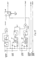
- BD is latched in a latch L1 whose output QL1 enables a second counter 82 and also initiates CMND via an AND gate 82.
- the counter 82 is a 4-bit command counter preset in accordance with the desired duration of CMND by CMND DATA. When this counter reaches its terminal count BC a second latch L2 latches BC and the QL2 BAR output of this latch disables the gate A2, so terminating CMND.
Landscapes
- Engineering & Computer Science (AREA)
- Microelectronics & Electronic Packaging (AREA)
- Computer Hardware Design (AREA)
- Static Random-Access Memory (AREA)
- Semiconductor Integrated Circuits (AREA)
- Oscillators With Electromechanical Resonators (AREA)
- Exchange Systems With Centralized Control (AREA)
- Memory System (AREA)
- Storage Device Security (AREA)
- Semiconductor Memories (AREA)
- Use Of Switch Circuits For Exchanges And Methods Of Control Of Multiplex Exchanges (AREA)
- Iron Core Of Rotating Electric Machines (AREA)
- Tests Of Electronic Circuits (AREA)
- Crystals, And After-Treatments Of Crystals (AREA)
- Non-Volatile Memory (AREA)
- Time-Division Multiplex Systems (AREA)
- Vehicle Body Suspensions (AREA)
- Amplifiers (AREA)
- Control Of Stepping Motors (AREA)
- For Increasing The Reliability Of Semiconductor Memories (AREA)
- Dram (AREA)
Applications Claiming Priority (2)
| Application Number | Priority Date | Filing Date | Title |
|---|---|---|---|
| GB8517699 | 1985-07-12 | ||
| GB8517699A GB2177825B (en) | 1985-07-12 | 1985-07-12 | Control system for chained circuit modules |
Related Parent Applications (2)
| Application Number | Title | Priority Date | Filing Date |
|---|---|---|---|
| EP86904286.1 Division | 1986-07-11 | ||
| EP86904286A Division-Into EP0231237B1 (de) | 1985-07-12 | 1986-07-11 | Steuersystem für gekettete schaltungsmodule |
Publications (2)
| Publication Number | Publication Date |
|---|---|
| EP0416714A2 true EP0416714A2 (de) | 1991-03-13 |
| EP0416714A3 EP0416714A3 (en) | 1991-08-07 |
Family
ID=10582224
Family Applications (2)
| Application Number | Title | Priority Date | Filing Date |
|---|---|---|---|
| EP19900202616 Withdrawn EP0416714A3 (en) | 1985-07-12 | 1986-07-11 | Wafer-scale integrated memory circuits |
| EP86904286A Expired - Lifetime EP0231237B1 (de) | 1985-07-12 | 1986-07-11 | Steuersystem für gekettete schaltungsmodule |
Family Applications After (1)
| Application Number | Title | Priority Date | Filing Date |
|---|---|---|---|
| EP86904286A Expired - Lifetime EP0231237B1 (de) | 1985-07-12 | 1986-07-11 | Steuersystem für gekettete schaltungsmodule |
Country Status (8)
| Country | Link |
|---|---|
| US (1) | US4943946A (de) |
| EP (2) | EP0416714A3 (de) |
| JP (2) | JPS63500545A (de) |
| KR (2) | KR880700423A (de) |
| AT (1) | ATE67890T1 (de) |
| DE (1) | DE3681724D1 (de) |
| GB (3) | GB2177825B (de) |
| WO (1) | WO1987000675A2 (de) |
Cited By (7)
| Publication number | Priority date | Publication date | Assignee | Title |
|---|---|---|---|---|
| WO1992022904A1 (en) * | 1991-06-13 | 1992-12-23 | The City University | Memory device |
| US5287345A (en) * | 1988-02-04 | 1994-02-15 | The City University | Data handling arrays |
| EP0698885A1 (de) * | 1994-08-26 | 1996-02-28 | STMicroelectronics Limited | Speicheranordnung |
| WO1998045787A1 (en) * | 1997-04-10 | 1998-10-15 | Advanced Micro Devices, Inc. | Pin count reduction through serialization techniques |
| US5933608A (en) * | 1988-02-04 | 1999-08-03 | The City University | Multiway signal switching device including a WSIC and optical communication ports |
| EP1050883A1 (de) * | 1999-05-03 | 2000-11-08 | STMicroelectronics SA | Schaltung zur Steuerung der Datenspeicherung |
| WO2005048270A1 (de) * | 2003-10-29 | 2005-05-26 | Infineon Technologies Ag | Integrierte schaltung, testsystem und verfahren zum auslesen eines fehlerdatums aus der integrierten schaltung |
Families Citing this family (28)
| Publication number | Priority date | Publication date | Assignee | Title |
|---|---|---|---|---|
| GB2184268B (en) * | 1985-12-13 | 1989-11-22 | Anamartic Ltd | Fault tolerant memory system |
| EP0424979A3 (en) | 1986-03-18 | 1991-07-03 | Anamartic Limited | Random address system for circuit modules |
| GB8713819D0 (en) * | 1987-06-12 | 1987-12-16 | Smiths Industries Plc | Information processing systems |
| US4798976A (en) * | 1987-11-13 | 1989-01-17 | International Business Machines Corporation | Logic redundancy circuit scheme |
| WO1989012320A1 (en) * | 1988-06-01 | 1989-12-14 | Anamartic Limited | Wafer scale integrated circuits |
| JP2516403B2 (ja) * | 1988-06-01 | 1996-07-24 | 富士通株式会社 | ウエハ・スケ―ル・メモリ |
| KR900003884A (ko) * | 1988-08-12 | 1990-03-27 | 미다 가쓰시게 | 대규모 반도체 집적회로 장치 |
| US5347450A (en) * | 1989-01-18 | 1994-09-13 | Intel Corporation | Message routing in a multiprocessor computer system |
| US5594866A (en) * | 1989-01-18 | 1997-01-14 | Intel Corporation | Message routing in a multi-processor computer system with alternate edge strobe regeneration |
| GB8903181D0 (en) * | 1989-02-13 | 1989-03-30 | Anamartic Ltd | Improvements relating to control systems for chained circuit modules |
| US5203005A (en) * | 1989-05-02 | 1993-04-13 | Horst Robert W | Cell structure for linear array wafer scale integration architecture with capability to open boundary i/o bus without neighbor acknowledgement |
| GB2234372A (en) * | 1989-07-18 | 1991-01-30 | Anamartic Ltd | Mass memory device |
| JP2522837B2 (ja) * | 1989-09-19 | 1996-08-07 | 富士通株式会社 | ウエハ・スケ―ル半導体装置 |
| JPH03106029A (ja) * | 1989-09-20 | 1991-05-02 | Fujitsu Ltd | ウエハ・スケール・ic |
| EP0509058A4 (en) * | 1990-01-05 | 1993-11-18 | Maspar Computer Corporation | Router chip with quad-crossbar and hyperbar personalities |
| GB2250359A (en) * | 1990-11-19 | 1992-06-03 | Anamartic Ltd | Addressing of chained circuit modules |
| US5467428A (en) * | 1991-06-06 | 1995-11-14 | Ulug; Mehmet E. | Artificial neural network method and architecture adaptive signal filtering |
| US6230245B1 (en) | 1997-02-11 | 2001-05-08 | Micron Technology, Inc. | Method and apparatus for generating a variable sequence of memory device command signals |
| US6175894B1 (en) | 1997-03-05 | 2001-01-16 | Micron Technology, Inc. | Memory device command buffer apparatus and method and memory devices and computer systems using same |
| US5996043A (en) * | 1997-06-13 | 1999-11-30 | Micron Technology, Inc. | Two step memory device command buffer apparatus and method and memory devices and computer systems using same |
| US6484244B1 (en) | 1997-06-17 | 2002-11-19 | Micron Technology, Inc. | Method and system for storing and processing multiple memory commands |
| US6202119B1 (en) | 1997-12-19 | 2001-03-13 | Micron Technology, Inc. | Method and system for processing pipelined memory commands |
| US6175905B1 (en) | 1998-07-30 | 2001-01-16 | Micron Technology, Inc. | Method and system for bypassing pipelines in a pipelined memory command generator |
| US6178488B1 (en) | 1998-08-27 | 2001-01-23 | Micron Technology, Inc. | Method and apparatus for processing pipelined memory commands |
| GB2379542B (en) * | 2000-09-05 | 2003-09-10 | Samsung Electronics Co Ltd | System comprising memory module |
| US7308524B2 (en) | 2003-01-13 | 2007-12-11 | Silicon Pipe, Inc | Memory chain |
| US9727267B1 (en) * | 2016-09-27 | 2017-08-08 | Intel Corporation | Power management and monitoring for storage devices |
| US10095432B2 (en) | 2016-09-27 | 2018-10-09 | Intel Corporation | Power management and monitoring for storage devices |
Family Cites Families (10)
| Publication number | Priority date | Publication date | Assignee | Title |
|---|---|---|---|---|
| GB1377859A (en) * | 1972-08-03 | 1974-12-18 | Catt I | Digital integrated circuits |
| US3882470A (en) * | 1974-02-04 | 1975-05-06 | Honeywell Inf Systems | Multiple register variably addressable semiconductor mass memory |
| US4038648A (en) * | 1974-06-03 | 1977-07-26 | Chesley Gilman D | Self-configurable circuit structure for achieving wafer scale integration |
| US3972031A (en) * | 1974-08-15 | 1976-07-27 | Zonic Technical Laboratories, Inc. | Variable length shift register alternately operable to store and recirculate data and addressing circuit therefor |
| US4020469A (en) * | 1975-04-09 | 1977-04-26 | Frank Manning | Programmable arrays |
| US4148099A (en) * | 1978-04-11 | 1979-04-03 | Ncr Corporation | Memory device having a minimum number of pins |
| GB2082354B (en) * | 1980-08-21 | 1984-04-11 | Burroughs Corp | Improvements in or relating to wafer-scale integrated circuits |
| GB2089536B (en) * | 1980-12-12 | 1984-05-23 | Burroughs Corp | Improvement in or relating to wafer scale integrated circuits |
| US4528647A (en) * | 1981-01-07 | 1985-07-09 | Burroughs Corp. | Wafer scale integrated circuit memories |
| GB2114782B (en) * | 1981-12-02 | 1985-06-05 | Burroughs Corp | Branched-spiral wafer-scale integrated circuit |
-
1985
- 1985-07-12 GB GB8517699A patent/GB2177825B/en not_active Expired
- 1985-10-15 GB GB08525324A patent/GB2178204B/en not_active Expired
-
1986
- 1986-07-11 WO PCT/GB1986/000401 patent/WO1987000675A2/en not_active Ceased
- 1986-07-11 EP EP19900202616 patent/EP0416714A3/en not_active Withdrawn
- 1986-07-11 AT AT86904286T patent/ATE67890T1/de not_active IP Right Cessation
- 1986-07-11 EP EP86904286A patent/EP0231237B1/de not_active Expired - Lifetime
- 1986-07-11 US US07/027,167 patent/US4943946A/en not_active Expired - Fee Related
- 1986-07-11 JP JP61503835A patent/JPS63500545A/ja active Pending
- 1986-07-11 JP JP61503992A patent/JPS63500618A/ja active Pending
- 1986-07-11 DE DE8686904286T patent/DE3681724D1/de not_active Expired - Fee Related
-
1987
- 1987-03-12 KR KR870700213A patent/KR880700423A/ko not_active Withdrawn
- 1987-03-12 KR KR870700212A patent/KR880700422A/ko not_active Withdrawn
-
1988
- 1988-08-17 GB GB8819599A patent/GB2207785B/en not_active Expired
Cited By (11)
| Publication number | Priority date | Publication date | Assignee | Title |
|---|---|---|---|---|
| US5287345A (en) * | 1988-02-04 | 1994-02-15 | The City University | Data handling arrays |
| US5933608A (en) * | 1988-02-04 | 1999-08-03 | The City University | Multiway signal switching device including a WSIC and optical communication ports |
| WO1992022904A1 (en) * | 1991-06-13 | 1992-12-23 | The City University | Memory device |
| EP0698885A1 (de) * | 1994-08-26 | 1996-02-28 | STMicroelectronics Limited | Speicheranordnung |
| US5687352A (en) * | 1994-08-26 | 1997-11-11 | Sgs-Thomson Microelectronics Limited | Memory device controlled by control signals in the form of gray code |
| WO1998045787A1 (en) * | 1997-04-10 | 1998-10-15 | Advanced Micro Devices, Inc. | Pin count reduction through serialization techniques |
| EP1050883A1 (de) * | 1999-05-03 | 2000-11-08 | STMicroelectronics SA | Schaltung zur Steuerung der Datenspeicherung |
| US6452857B1 (en) | 1999-05-03 | 2002-09-17 | Stmicroelectronics S.A. | Circuits for controlling the storage of data into memory |
| WO2005048270A1 (de) * | 2003-10-29 | 2005-05-26 | Infineon Technologies Ag | Integrierte schaltung, testsystem und verfahren zum auslesen eines fehlerdatums aus der integrierten schaltung |
| US7434125B2 (en) | 2003-10-29 | 2008-10-07 | Infineon Technologies Ag | Integrated circuit, test system and method for reading out an error datum from the integrated circuit |
| KR100868119B1 (ko) * | 2003-10-29 | 2008-11-10 | 인피니언 테크놀로지스 아게 | 집적 회로, 테스트 시스템, 에러 데이터 판독 방법 |
Also Published As
| Publication number | Publication date |
|---|---|
| KR880700422A (ko) | 1988-03-15 |
| GB8517699D0 (en) | 1985-08-21 |
| GB2177825B (en) | 1989-07-26 |
| DE3681724D1 (de) | 1991-10-31 |
| WO1987000675A2 (en) | 1987-01-29 |
| EP0231237A1 (de) | 1987-08-12 |
| JPS63500618A (ja) | 1988-03-03 |
| US4943946A (en) | 1990-07-24 |
| GB2177825A (en) | 1987-01-28 |
| GB8819599D0 (en) | 1988-09-21 |
| WO1987000675A3 (en) | 1987-03-26 |
| EP0231237B1 (de) | 1991-09-25 |
| GB2207785B (en) | 1989-07-26 |
| ATE67890T1 (de) | 1991-10-15 |
| JPS63500545A (ja) | 1988-02-25 |
| GB2178204A (en) | 1987-02-04 |
| EP0416714A3 (en) | 1991-08-07 |
| GB2178204B (en) | 1988-11-16 |
| GB2207785A (en) | 1989-02-08 |
| KR880700423A (ko) | 1988-03-15 |
| GB8525324D0 (en) | 1985-11-20 |
Similar Documents
| Publication | Publication Date | Title |
|---|---|---|
| EP0231237B1 (de) | Steuersystem für gekettete schaltungsmodule | |
| US5072424A (en) | Wafer-scale integrated circuit memory | |
| US5325337A (en) | Random access memories (RAM) and more particularly to self-timed RAMS | |
| EP0264893B1 (de) | Halbleiterspeicher | |
| US6876228B2 (en) | Field programmable gate array | |
| KR100518397B1 (ko) | 반도체 메모리 장치 및 제어 방법 | |
| US6262937B1 (en) | Synchronous random access memory having a read/write address bus and process for writing to and reading from the same | |
| US4882710A (en) | FIFO memory including dynamic memory elements | |
| US4989181A (en) | Serial memory device provided with high-speed address control circuit | |
| US5943252A (en) | Content addressable memory | |
| US20190392891A1 (en) | Bi-directional input/output enable signal propagation structure and method | |
| US4847615A (en) | Control system for chained circuit modules | |
| US12518809B2 (en) | Memory device with write circuit and method of operating the same | |
| WO2005031746A2 (en) | Random access memory with post-amble data strobe signal noise rejection | |
| EP0248875A1 (de) | Fehlertolerantes speichersystem | |
| US4577292A (en) | Support circuitry for multi-port systems | |
| JP2610598B2 (ja) | 半導体メモリへのデータの並列書込み回路装置 | |
| US6477625B1 (en) | Method and system for reading a memory by applying control signals thereto | |
| US5963482A (en) | Memory integrated circuit with shared read/write line | |
| US12272427B2 (en) | Semiconductor device including first and second clock generators | |
| US20250364024A1 (en) | Method, device, and circuit for high-speed memories | |
| US20060268651A1 (en) | Memory apparatus and method | |
| JPH04219691A (ja) | 半導体メモリ装置 | |
| HK1008758B (en) | Self-timed random access memories | |
| JPH0581854A (ja) | モノリシツク記憶装置 |
Legal Events
| Date | Code | Title | Description |
|---|---|---|---|
| PUAI | Public reference made under article 153(3) epc to a published international application that has entered the european phase |
Free format text: ORIGINAL CODE: 0009012 |
|
| 17P | Request for examination filed |
Effective date: 19901221 |
|
| AC | Divisional application: reference to earlier application |
Ref document number: 231237 Country of ref document: EP |
|
| AK | Designated contracting states |
Kind code of ref document: A2 Designated state(s): AT BE CH DE FR IT LI NL SE |
|
| PUAL | Search report despatched |
Free format text: ORIGINAL CODE: 0009013 |
|
| AK | Designated contracting states |
Kind code of ref document: A3 Designated state(s): AT BE CH DE FR IT LI NL SE |
|
| 17Q | First examination report despatched |
Effective date: 19930812 |
|
| STAA | Information on the status of an ep patent application or granted ep patent |
Free format text: STATUS: THE APPLICATION IS DEEMED TO BE WITHDRAWN |
|
| 18D | Application deemed to be withdrawn |
Effective date: 19931223 |