EP0413966A2 - Pulse width modulation type inverter having temperature compensation - Google Patents
Pulse width modulation type inverter having temperature compensation Download PDFInfo
- Publication number
- EP0413966A2 EP0413966A2 EP90113857A EP90113857A EP0413966A2 EP 0413966 A2 EP0413966 A2 EP 0413966A2 EP 90113857 A EP90113857 A EP 90113857A EP 90113857 A EP90113857 A EP 90113857A EP 0413966 A2 EP0413966 A2 EP 0413966A2
- Authority
- EP
- European Patent Office
- Prior art keywords
- frequency
- output
- carrier frequency
- inverter
- carrier
- Prior art date
- Legal status (The legal status is an assumption and is not a legal conclusion. Google has not performed a legal analysis and makes no representation as to the accuracy of the status listed.)
- Granted
Links
Images


Classifications
-
- H—ELECTRICITY
- H02—GENERATION; CONVERSION OR DISTRIBUTION OF ELECTRIC POWER
- H02M—APPARATUS FOR CONVERSION BETWEEN AC AND AC, BETWEEN AC AND DC, OR BETWEEN DC AND DC, AND FOR USE WITH MAINS OR SIMILAR POWER SUPPLY SYSTEMS; CONVERSION OF DC OR AC INPUT POWER INTO SURGE OUTPUT POWER; CONTROL OR REGULATION THEREOF
- H02M7/00—Conversion of ac power input into dc power output; Conversion of dc power input into ac power output
-
- H—ELECTRICITY
- H02—GENERATION; CONVERSION OR DISTRIBUTION OF ELECTRIC POWER
- H02P—CONTROL OR REGULATION OF ELECTRIC MOTORS, ELECTRIC GENERATORS OR DYNAMO-ELECTRIC CONVERTERS; CONTROLLING TRANSFORMERS, REACTORS OR CHOKE COILS
- H02P27/00—Arrangements or methods for the control of AC motors characterised by the kind of supply voltage
- H02P27/04—Arrangements or methods for the control of AC motors characterised by the kind of supply voltage using variable-frequency supply voltage, e.g. inverter or converter supply voltage
- H02P27/06—Arrangements or methods for the control of AC motors characterised by the kind of supply voltage using variable-frequency supply voltage, e.g. inverter or converter supply voltage using dc to ac converters or inverters
- H02P27/08—Arrangements or methods for the control of AC motors characterised by the kind of supply voltage using variable-frequency supply voltage, e.g. inverter or converter supply voltage using dc to ac converters or inverters with pulse width modulation
-
- H—ELECTRICITY
- H02—GENERATION; CONVERSION OR DISTRIBUTION OF ELECTRIC POWER
- H02M—APPARATUS FOR CONVERSION BETWEEN AC AND AC, BETWEEN AC AND DC, OR BETWEEN DC AND DC, AND FOR USE WITH MAINS OR SIMILAR POWER SUPPLY SYSTEMS; CONVERSION OF DC OR AC INPUT POWER INTO SURGE OUTPUT POWER; CONTROL OR REGULATION THEREOF
- H02M7/00—Conversion of ac power input into dc power output; Conversion of dc power input into ac power output
- H02M7/42—Conversion of dc power input into ac power output without possibility of reversal
- H02M7/44—Conversion of dc power input into ac power output without possibility of reversal by static converters
- H02M7/48—Conversion of dc power input into ac power output without possibility of reversal by static converters using discharge tubes with control electrode or semiconductor devices with control electrode
- H02M7/53—Conversion of dc power input into ac power output without possibility of reversal by static converters using discharge tubes with control electrode or semiconductor devices with control electrode using devices of a triode or transistor type requiring continuous application of a control signal
- H02M7/537—Conversion of dc power input into ac power output without possibility of reversal by static converters using discharge tubes with control electrode or semiconductor devices with control electrode using devices of a triode or transistor type requiring continuous application of a control signal using semiconductor devices only, e.g. single switched pulse inverters
- H02M7/539—Conversion of dc power input into ac power output without possibility of reversal by static converters using discharge tubes with control electrode or semiconductor devices with control electrode using devices of a triode or transistor type requiring continuous application of a control signal using semiconductor devices only, e.g. single switched pulse inverters with automatic control of output wave form or frequency
- H02M7/5395—Conversion of dc power input into ac power output without possibility of reversal by static converters using discharge tubes with control electrode or semiconductor devices with control electrode using devices of a triode or transistor type requiring continuous application of a control signal using semiconductor devices only, e.g. single switched pulse inverters with automatic control of output wave form or frequency by pulse-width modulation
Definitions
- the present invention relates to a pulse width modulation type inverter for delivering an A.C. current at variable voltage and variable frequency. More particularly, the present invention is concerned with the control of the pulse width modulation signal (referred to as a "PWM" signal, hereinafter) in an inverter using a high carrier frequency.
- PWM pulse width modulation signal
- FIG 10 is an illustration of the arrangement of a conventional PWM inverter.
- the known PWM inverter includes a D.C. power supply 100 and an inversion converter 200 composed of a controllable element and a pair of inverse parallel-connected diodes.
- the inversion converter is capable of converting a D.C. current into an A.C. current of variable voltage and variable frequency, which is useable to drive an electric motor 300, or similar device.
- a reference voltage generator 400 generates a reference voltage waveform, which is used as a reference for the output frequency and output voltage. In practice, the waveform of the reference voltage has the optimum shape for operating the motor, but such a shaped waveform cannot be obtained with adequate power where commercial electrical power is not available.
- a carrier waveform having adequate power is mixed with the reference wave and results in a pulsed waveform having the same area as the reference voltage wave, adequate to drive the motor or like device.
- the reference waveform is modified in response to the input from an output frequency setting device 900 that is setable by a user.
- a suitable carrier generator 500 will form a carrier signal, for example, a triangular waveform, at a frequency f c .
- a PWM circuit 600 is operative in response to the signals from the reference voltage generator 400 and the carrier generator 500 to produce a control signal for the controllable element of the inversion converter 200.
- a driving circuit 700 will drive the controllable element of the inversion converter 200 in response to the signal from the PWM circuit 600 and an output frequency setting device 900.
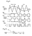
- FIG. 11 illustrates several waveforms that occur during a typical PWM operation.
- the illustration is in regard to only one phase, specifically the "U phase", of the three phases U, V and W relevant to the actual inverter operation in producing 3-phase A.C. power for operating a motor or like device.
- the triangular waveform output of the carrier generator 500 and the sinusoidal waveform output by the reference voltage generator 400 are shown superimposed in the same time frame.
- the superimposed waveforms illustrate a comparison between the reference voltage, which is used as a reference for the output voltage and the output frequency of the inverter, and the signal for modulating the reference voltage, e.g.
- Waveforms in Figure 11(b) are generated on the basis of the points of the waveforms of Figure 11(a) where the reference voltage waveform and the carrier cross.
- One of the waveforms in Figure 11(b) is a PWM signal U po This signal is generated for the upper side of the U phase and the signal is ON in the period in which the reference voltage is higher than the carrier voltage and OFF in the period in which the reference voltage is lower than that of the carrier.
- the other waveform in Figure 11(b) is a PWM signal U NO . This signal is generated for the lower side of the U phase and is obtained as the inversion of the signal U PO .
- the controllable element is actually driven by the PWM signals Up and Un, as seen in Figure 11(c), which signals are formed from waveforms U PO and U NO as subjected to a short circuit prevention process which delays the timing of the ON pulse by a time duration T d .
- T d the pulse-width modulated output voltage obtained as the U phase output is shown in Figure 11(d). Similar outputs are obtained for the V and W phases.
- the reference voltage waveform shown in Figure 11(a) which provides a reference for output frequency and output voltage, is delivered by the reference voltage waveform generator 400.
- the triangular carrier wave shown in Figure 11(a) is generated by the carrier generator 500.
- the PWM circuit 600 responds to the waveforns of Figure 11(a) and generates a PWM signal as shown in Figure 11(c).
- the driving circuit 700 amplifies the output of circuit 600 and drives the controllable element of the inversion converter 200 accordingly. Since the driving signal will vary with changes in the reference voltage waveform, an A.C. current may be obtained from the inverter with a variable voltage and a variable frequency.
- a high-speed switching element such as a power MOSFET, IGBT or the like, operable at a frequency between 10-20 Khz.
- the "ordinary loss” is the product of the current flowing during the ON time and the voltage drop
- the “switching loss” is the product of voltage and current at the time that the controllable element is turned ON and OFF.
- the total ordinary loss P ON is merely a function of current level (I)
- the total switching loss P SW is a function of current level (I) and the carrier frequency (f c ) which controls the switching of the element.
- the switching loss P SW is increased as the carrier frequency f c is increased. Also, the ratio of loss P ON : P SW is large when the current is near the level of the rated current of the inverter.
- inverter operation results in a relatively high switching loss, i.e ., high f c and high current, since proper thermal design of the switching element requires that its junction temperature be maintained below a given level, there is a significant cooling requirement.
- operation of the inverter at a high carrier frequency will reduce audible noise, but will require both an increase in the cooling capability and the size of the inverter.
- the noise produced poses a serious problem when an inverter-driven electric motor operates at low speed.
- the noise generated by the load driven by the motor is relatively low and the motor noise tends to be dominant.
- the noise generated by the load driven by the motor is increased so that the higher harmonic sounds produced by the electric motor are not dominant and their effect is not critical.
- f c is maintained high so that the loss is increased due to high switching losses.
- the conventional inverter In order to satisfy the thermal requirements of the switching element, the conventional inverter must be designed to maintain the temperature of the switching element below a maximum allowable temperature.
- the inverter can operate safely even when f c is kept high after an increase in the load.
- the most effective parameter available to contain the temperature below the maximum for the switching element is the carrier frequency f c . If carrier frequency f c is reduced to reduce the temperature rise due to switching power losses, however, it is difficult to effectively suppress the generation of audible noise.
- an object of the present invention is to provide an inverter apparatus which can operate with a lowered level of audible noise and which can compensate for increases in loss without requiring the size of the inverter to be increased or special cooling to be applied.
- a further object of the present invention is to control the carrier frequency in accordance with the inverter output frequency or the temperature of the controllable elements, or output current, so that the generation of noise is suppressed and the loss of power is reduced.
- the carrier frequency is variable within a range between an upper limit carrier frequency f c max, which is determined by the acceptable loss and the response time of the inverter, and a lower limit carrier frequency f c min, which is determined by the acceptable noise characteristic and distortion of the output current.
- the carrier frequency is controlled in accordance with the temperature of the controllable element of the inverter apparatus in such a manner that the carrier frequency is decreased and increased, respectively, as the detected temperature of the controllable element is increased and decreased.
- the carrier frequency is controlled in accordance with the output frequency of the inverter apparatus in such a manner that the carrier frequency is decreased and increased, respectively, as the inverter output frequency is increased and decreased.
- the carrier frequency may also be controlled in accordance with the output current of the inverter apparatus in such a manner that the carrier frequency is decreased and increased, respectively, as the inverter output current is increased and decreased.
- the carrier generator in the inverter apparatus of the present invention determines the carrier frequency in accordance with the temperature of the controllable element of the inverter or the output frequency or output current of the inverter. More specifically, the carrier frequency is increased when the detected temperature or the speed of the electric motor is low or the inverter output current is small, to thereby suppress noise generation, whereas when the detected temperature or the motor speed is increased or the inverter output current is large, the carrier frequency is decreased so as to reduce loss generated in the controllable element.
- numerals 100, 200, 300, 400, 600, 700 and 900 indicate elements which are the same or similar to those denoted by the same numerals in Figure 10, referring to the known inverter apparatus.
- Numeral 800 denotes a temperature detector for detecting the temperature of the controllable element and
- numeral 501 denotes a carrier generator that produces a signal with a frequency f c that is variable in response to the output of the temperature detector 800.
- the carrier frequency f c is controlled in a linear manner as shown in Figure 3, within a range between predetermined frequency limits f c max and f c min, in accordance with changes in temperature To, as represented by the output from the temperature detector 800.
- a carrier for example, a triangular waveform, is delivered to the PWM circuit at the controlled carrier frequency f c .
- FIG 2 shows another embodiment of the present invention.
- the elements of this embodiment are substantially the same as that shown in Figure 1 except that the temperature detector is removed and carrier generator 501 receives instead an input from the inverter output frequency setting device 900.
- the carrier frequency f c is controlled in a linear manner shown in Figure 4, within a range between predetermined frequency limits f c max and f c min, in accordance with changes in output frequency f o .
- the output frequency is set by an operator (i.e.
- Figure 12 shows a third embodiment in which the carrier frequency is controlled in accordance with the output from a current detector 1000, capable of detecting the load current on the inverter, within a range of low current I oc and high current I oH .
- the carrier frequency has an inverse linear relationship with the current within a range between predetermined frequencies f c max and f c min, (typically 15 Khz - 20 Khz) in a manner shown in Figure 13.
- the current detector 1000 may be a DCCT current detector which makes use of a Hall element. Although in Figure 13 the current detector 1000 is provided at the output side of the inverter, this is only illustrative and the current detector 1000 may be provided at any suitable portion where it can detect a current corresponding to the output current of the inverter.
- the motor which is the load on the inverter generates a higher-harmonic noise attributable to the carrier frequency f c .
- the effect of the noise can be avoided by increasing the carrier frequency f c to a level higher than the range of audible frequencies.
- Such a countermeasure causes a significant increase in the loss in the controllable element, causing a risk that the temperature T o of the controllable element will exceed the allowable upper limit value.
- T o Ta + T (2)
- Ta represents the temperature of the ambient air around the inverter
- T represents the temperature rise of the controllable element itself.
- T P x R th (3)
- P the loss of the controllable element
- R th the thermal resistance of the controllable element including its cooling means.
- the loss P generated in the controllable element can be expressed in terms of the steady loss P ON and switching loss P SW , wherein the steady loss P ON can be given as a function of the output current I O , while the switching loss P SW is a function of the output current I O and the carrier frequency f c .
- the loss P is changed in relation to the power P L supplied by the inverter to the load: namely, the smaller the power P L , the smaller the loss P.
- one aim of the use of an inverter of the type described resides in the reduction of energy consumption by reducing the power P L supplied to the load by reducing the output frequency f o of the inverter. In consequence, it is possible to reduce the loss P by reducing the output frequency f o and the loss P can be expressed as a function of the output frequency f o .
- T O T a + ⁇ P ON (I O , f o ) + P SW (I O , f c ) ⁇ x R th (4)
- the temperature T o of the controllable element can be determined when the ambient air temperature T a around the inverter, output current I O , output frequency f o and the carrier frequency f c are given.
- the parameters other than the carrier frequency f c are determined by the conditions and environment under which the inverter is used and, hence, cannot be controlled by the inverter itself.
- the temperature T O of the controllable element may rise as a result of one or both of the loss generated in the controllable element due to a change in the conditions or environment under which the inverter is used and a rise in the ambient air temperature around the inverter.
- the carrier frequency f c when the temperature T O approaches the maximum allowable temperature T R of the controllable element, the carrier frequency f c is lowered so as to maintain the temperature T O of the controllable element below the maximum allowable temperature T R .
- Figure 3 qualitatively illustrates the relationship between frequency and temperature and shows that frequency must be reduced to reduce the temperature.
- temperature is detected indirectly through detection of the output frequency f o and the output current I O .
- the control is not as accurate when compared with the method which relies upon the direct detection of the temperature T O of the controllable element.
- Such systems can be constructed with reduced cost because no temperature sensor is required.
- carrier generator 501 In Figure 5, the details of carrier generator 501 are shown.
- a reference voltage generator 3 whose output approximates a sine wave by, for example, quantization of an input analog signal with n-bit digital processing.
- Reference numeral 4 denotes a device for generating the upper limit value of a triangular wave carrier signal, having a controllable upper limit value, while numeral 5 denotes a device for generating the lower limit value of the triangular carrier signal.
- the devices 3 to 5 can be realized by the computing functions of a microcomputer 6, which may output respective voltage values in digital form.
- the microcomputer 6 may be a 16-bit microcomputer such as INTEL 8096 CPU, having a 16 bit data bus and incorporating an A/D converter.
- the voltage data derived from the microcomputer 6 are latched by flip-flops 7-9.
- the inverter of this embodiment is assumed to output 3-phase A.C. power so that flip-flops 7-9 latch voltages applicable to each of the U, V and W phases.
- Flip-flops 10 and 11 are connected to the microcomputer 6 for latching the upper and lower limit value data outputs from the limit generating elements 4 and 5, respectively.
- CS1, CS2, CS3, CS4 and CS5 represent control signals from the microcomputer 6 to the flip-flops 7 to 11.
- An n-bit up-and-down counter 12 is used for quantizing the triangular waveform generated by the carrier signal generator and outputting the quantized value.
- the triangular waveform is generated by counter 13, which repeats an up-count CKU and a down-count CKD in response to a clock input signal CK.
- Numerals 14 to 18 denote n-bit digital signal comparators. More specifically, the comparator 14 compares the n-bit U-phase voltage data from flip-flop 7 with the n-bit triangular wave data output by counter 12 and produces an output signal UP o in accordance with the result of the comparison.
- Comparator 17 is operative to compare the triangular wave data produced by the up-and-down counter 12 with the triangular wave upper limit data derived from the flip-flop 10 and delivers an output signal EQ u to the clock switching circuit 13.
- the output signals from the digital comparators 14, 15 and 16 which serve as signals for driving the switching elements of the U-, V- and W-phase are delivered to inversion circuits and short-circuit prevention circuits (not shown) in the manner illustrated for one of the phase signals in Figure 12.
- An output frequency setting device 1 and a temperature detector 2 are also seen in Figure 5, connected to microcomputer 6.
- the output frequency setting device 1 may output a signal in the form of voltage or current, based upon the operator's setting of a variable control contact in the device.
- the output frequency setting device 1 operates with a voltage signal.
- the temperature detector 2 for detecting the temperature of a switching element, e.g., a MOSFET or IGBT, outputs an analog signal, e.g, a voltage signal.
- the temperature detector may be a switch which is turned “on” and “off” when the temperature changes across a reference temperature.
- the output signal from the output frequency setting device 1 or the temperature detector 2 is delivered to the input port of the microcomputer 6.
- a voltage signal is input from the output frequency setting device 1
- a reference voltage corresponding to the output frequency is output from the microcomputer 6.
- the triangular wave upper and lower limit values which provide turning points of the triangular wave, are output from the microcomputer 6.
- the output signal from the output frequency setting device 1 or the temperature detector 2 is delivered to the input port of the microcomputer 6 which converts the thus input analog signal into a digital signal and calculates the upper and lower limit values of the reference voltage triangular wave. It is assumed here that the level of the output from the output frequency setting device 1 or temperature detection device 2 is constant.
- the microcomputer 6 can output a sine wave reference signal, quantized and approximated by an n-bit digital amount, as shown in Figure 6.
- the imaginary center of the amplitude of this sine wave resides between 200H and 1FFH in terms ot hexadecimal notation and the output sine wave changes its amplitude about this center of amplitude.
- the output frequency setting device 1 sets the output frequency of the inverter apparatus to a high level
- the sine waveform amplitude is increased.
- the output frequency is set to a low level
- the amplitude is decreased.
- the voltage signals computed and output by the microcomputer 6 are latched by flip-flops 7, 8 and 9, in correspondence with the voltages of the three phases U, V and W, respectively. These voltage data are set and latched at 120° intervals in terms of electric angle.
- the voltage data would be set through the 16-bit data bus of the microcomputer 6, when the size of the voltage data of each of U, V and W phases exceeds 5 bits, the voltage data cannot be set and latched in one operation, and the setting and latching has to be done in a plurality of operations. In such a case, the comparison of these voltage data with the triangular wave performed by the comparators is impeded due to the time difference existing between the voltage data for the three different phases. It is therefore necessary to provide an additional stage of flip-flops so as to enable the provision of voltage data for the U, V and W phases sinultaneously.
- the triangular wave upper and lower limit value data output from the microcomputer 6, as a result of functions 4 and 5, respectively, provide the turning points of the triangular wave generated by the triangular wave generator 12.
- the triangular wave upper limit value is latched by the flip-flop 10 and delivered to the comparator 17.
- the triangular wave lower limit value is latched by the flip-flop 11 and delivered to the comparator 18.
- the triangular wave generator 12 is an up-and-down counter which is controlled by up-counting clock CKU and down-counting clock CKD, and its current count is output simultaneously to comparators 14-18.
- the up-and-down counter 12 If the up-and-down counter 12 is in up-counting mode, it continues to count up in response to input clock signals CKU as seen by the ascending step waveform of Figure 7. However, when the triangular wave data constituted by n bits has become equal to the n-bit triangular wave upper limit value during the up-counting by the counter 12, the comparator 17 produces a coincidence signal EQU. In response to this signal EQU, the clock switching circuit 13 operates to set the up-count clock CKU in a non-active state and set the down-count clock CKD in an active state, so that the counter 12 is switched from up-counting mode to down-counting mode.
- the counter 12 When in the down-counting mode, the counter 12 counts down from its value at the turning point in stepped response to clock input CKD, as also seen in Figure 7.
- the comparator circuit 18 delivers a coincidence signal EQD.
- the clock switching circuit 13 operates so that the clock CKD and the clock CKU are switched into inactive and active states, respectively. The above-described operation is continually repeated so that a triangular wave signal is formed which has crests at the level of the triangular wave upper limit value and valleys at the level of the triangular wave lower limit value.
- Figure 8 shows an example of the construction of the clock switching circuit used in counter 13.
- the upper limit coincidence signal EQU and the lower limit coincidence signal EQD are amplified by amplifiers 131 and 132, respectively, and are input to set-reset type flip-flop 133.
- the Q output of the flip-flop is divided into two signals, one of which is inverted by inverter amplifier 134.
- a pair of logic gates 135 and 136 receive clock signal CK and each gate receives one of the Q signal and a signal which is the inversion of Q .
- the gates produce the clocks CKU and CKD.
- the frequency of the triangular wave is determined by the set values of the upper and lower limits and the frequency f ck of the clock CK with which frequency the up-and-down counter 12 performs its counting function.
- the following formula determines the frequency: If it is assumed that the triangular wave data is 10-bit data with upper and lower limit values of 3FFH and 000H in terms of hexadecimal notation, while the frequency f ck is 20 Mhz, the frequency of the triangular wave, i.e., the carrier frequency f c , is calculated from formula (5) as follows:
- the carrier frequency may be changed in accordance with the information from the output frequency setting device 1.
- the carrier frequency f c i.e ., the frequency of the triangular wave
- the carrier frequency f c can be controlled by varying the upper and lower limit values provided that the clock frequency f ck is constant. For instance, if the upper and lower limits are set to 2 FFH and 100H, respectively, the carrier frequency f c is calculated from formula (1) as follows:
- the carrier frequency f c by reducing the difference k between the upper and lower limit values. It is therefore possible to control the carrier frequency f c in relation to the output frequency of the inverter in such a manner that the carrier frequency f c is decreased and increased, respectively, in response to an increase and decrease in the inverter output frequency, by setting the output from the microcomputer 6 in such a manner as to decrease and increase the value of the difference k in response to increases and decreases in the inverter output frequency.
- the control of the carrier frequency f c in response to the detected temperature can be executed in the same manner. Namely, the temperature value input from temperature detector 1 can be used by microcomputer 6 to adjust the value k by adjusting either or both upper and lower limit values of the triangular waveform.
- the amplitude of the triangular wave is maintained constant so that the amplitude of the reference voltage is changed in proportion to the frequency of the reference voltage and delivered as the output from the inverter apparatus.
- the relationship between the voltage and the frequency of the A.C. power is determined by the amplitude of the triangular wave, the amplitude of the reference voltage and the frequency of the reference voltage.
- the amplitude of the triangular wave is changed in accordance with a change in the carrier frequency f c so that the amplitude of the reference voltage is also changed in order to maintain a constant relationship between the voltage and frequency of the output A.C. power of the inverter apparatus.
- each of the flip-flops 7 to 11 can be realized by D-type flip-flops 74HC74, each of the comparators 14 to 18 can be realized by a magnitude comparator 74HC85, and the up-and-down counter 12 can be realized by an up-and-down binary counter 74HC193.
- a change in the frequency of the triangular wave without being accompanied by a change in the amplitude can be realized simply by changing the clock frequency f ck .
- controllable elements While the temperature of the controllable elements is detected directly in the described embodiments, it may be more practical to detect the temperature of the surface of the cooling construction of the controllable elements or a part thereof, and to detect the ambient temperature of the inverter.
- the automatic control of carrier frequency in response to detected temperature can readily be achieved by microcomputer 6.
- Figure 15 schematically shows the flow of the process for changing the carrier frequency f c upon detection of the element temperature T O as performed by the microcomputer 6.
- the step START represents that the operation of the inverter is started. Considering that the element temperature T O is still low, f c max is set as the carrier frequency f c in Step S1. Taking into account the carrier frequency f c max, setting of the reference voltage, setting of the upper limit value of the triangular wave and the setting of the lower limit value are executed in Steps S2 to S4.
- Step S5 a time process is performed by a timer in which a time t1 has been set.
- the time t1 is determined on the basis of the thermal time constant of the controllable element including the cooling means of the controllable element.
- the element temperature T O is read in Step S6.
- Step S7 the element temperature T O is compared with the command temperature T.
- the command temperature T is a value obtained from the thermal design of the controllable element. In general, the command temperature T is set at a level which is obtained by de-rating the allowable maximum temperature T R to some extent.
- the carrier frequency f c is set in Step S8 to a level which is higher than the instant carrier frequency f c by f c .
- Steps S2 to S4 are executed again on the basis of the carrier frequency f c set in Step S8 or S9, and this operation is conducted repeatedly.
- Step S8 allows the operation of the inverter to continue by setting the frequency increment f c to zero, i.e ., maintaining the carrier frequency f c constantly at the level of the f c max.
- Step S9 the microcomputer judges that an abnormal temperature rise of the element is taking place, and skips to a protection process routine.
- Figure 16 quantitatively shows the manner in which the carrier frequency f c and the element temperature T O are changed in relation to the time t as a result of execution of the process described hereinabove.
- the described embodiment may be modified such that a tolerance T is imparted to the command temperature T so as to give a hysteresis effect to the control of the carrier frequency f c . It is also possible to compute the variance of the detected element temperature T O and to vary the carrier frequency increment f c in accordance with the variance of the element temperature.
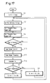
- Figure 17 schematically shows the flow of the process performed by the microcomputer 6 for changing the carrier frequency f c on the basis of the output current I O and the output frequency f o .
- the process is materially the same as that shown in Figure 15 except that T o is computed from the detected values I O and f o of the output current and the output frequency instead of being detected directly.
Abstract
Description
- The present invention relates to a pulse width modulation type inverter for delivering an A.C. current at variable voltage and variable frequency. More particularly, the present invention is concerned with the control of the pulse width modulation signal (referred to as a "PWM" signal, hereinafter) in an inverter using a high carrier frequency.
- Figure 10 is an illustration of the arrangement of a conventional PWM inverter. Referring to the drawings, the known PWM inverter includes a
D.C. power supply 100 and aninversion converter 200 composed of a controllable element and a pair of inverse parallel-connected diodes. The inversion converter is capable of converting a D.C. current into an A.C. current of variable voltage and variable frequency, which is useable to drive anelectric motor 300, or similar device. Areference voltage generator 400 generates a reference voltage waveform, which is used as a reference for the output frequency and output voltage. In practice, the waveform of the reference voltage has the optimum shape for operating the motor, but such a shaped waveform cannot be obtained with adequate power where commercial electrical power is not available. Thus, a carrier waveform having adequate power is mixed with the reference wave and results in a pulsed waveform having the same area as the reference voltage wave, adequate to drive the motor or like device. The reference waveform is modified in response to the input from an outputfrequency setting device 900 that is setable by a user. Asuitable carrier generator 500 will form a carrier signal, for example, a triangular waveform, at a frequency fc. APWM circuit 600 is operative in response to the signals from thereference voltage generator 400 and thecarrier generator 500 to produce a control signal for the controllable element of theinversion converter 200. Adriving circuit 700 will drive the controllable element of theinversion converter 200 in response to the signal from thePWM circuit 600 and an outputfrequency setting device 900. - The operation of this known inverter will be described with reference to Figure 11, which illustrates several waveforms that occur during a typical PWM operation. It should be noted that the illustration is in regard to only one phase, specifically the "U phase", of the three phases U, V and W relevant to the actual inverter operation in producing 3-phase A.C. power for operating a motor or like device. Referring to Figure 11(a), the triangular waveform output of the
carrier generator 500 and the sinusoidal waveform output by thereference voltage generator 400 are shown superimposed in the same time frame. The superimposed waveforms illustrate a comparison between the reference voltage, which is used as a reference for the output voltage and the output frequency of the inverter, and the signal for modulating the reference voltage, e.g., the triangular carrier waveform. Waveforms in Figure 11(b) are generated on the basis of the points of the waveforms of Figure 11(a) where the reference voltage waveform and the carrier cross. One of the waveforms in Figure 11(b) is a PWM signal Upo This signal is generated for the upper side of the U phase and the signal is ON in the period in which the reference voltage is higher than the carrier voltage and OFF in the period in which the reference voltage is lower than that of the carrier. The other waveform in Figure 11(b) is a PWM signal UNO. This signal is generated for the lower side of the U phase and is obtained as the inversion of the signal UPO. The controllable element is actually driven by the PWM signals Up and Un, as seen in Figure 11(c), which signals are formed from waveforms UPO and UNO as subjected to a short circuit prevention process which delays the timing of the ON pulse by a time duration Td . As a result of this delay, the pulse-width modulated output voltage obtained as the U phase output is shown in Figure 11(d). Similar outputs are obtained for the V and W phases. - Referring again to Figure 10, the reference voltage waveform shown in Figure 11(a), which provides a reference for output frequency and output voltage, is delivered by the reference
voltage waveform generator 400. The triangular carrier wave shown in Figure 11(a) is generated by thecarrier generator 500. ThePWM circuit 600 responds to the waveforns of Figure 11(a) and generates a PWM signal as shown in Figure 11(c). Thedriving circuit 700 amplifies the output ofcircuit 600 and drives the controllable element of theinversion converter 200 accordingly. Since the driving signal will vary with changes in the reference voltage waveform, an A.C. current may be obtained from the inverter with a variable voltage and a variable frequency. - When an electric motor is driven with this type of PWM waveform, higher harmonics, in the audible range, are generated due to the carrier frequency. These audible signals will increase the level of noise in a work environment. One countermeasure for averting this problem is to increase the carrier frequency to the upper limit of the human audible frequency range (i.e., 15 KHz) or higher. The level of noise will progressively decrease as the carrier frequency is increased. In fact, when the carrier frequency is within the range between 10 KHz and 15 KHz, the noise frequency approaches the upper limit of the audible frequency range and the noise level is lowered. When the carrier frequency is increased beyond 20 Khz the audible frequency range is exceeded so that the higher harmonics are not detectable by human ears. As a result, the noise level is reduced almost to the level produced when the load is driven by commercial electrical power.
- In order to achieve a high carrier frequency accompanied by low noise, a high-speed switching element such as a power MOSFET, IGBT or the like, operable at a frequency between 10-20 Khz, may be used. The disadvantage of such design is that the switching is inevitably accompanied by a significant amount of power loss. More specifically, the loss P generated by a controllable element accompanied by inverse-parallel diodes, is given by the following formula:
P = PON + PSW
= ordinary loss + switching loss
= PON (I) + PSW (fc, I) (1) - The "ordinary loss" is the product of the current flowing during the ON time and the voltage drop, while the "switching loss" is the product of voltage and current at the time that the controllable element is turned ON and OFF. In simplified form, as indicated in equation (1), the total ordinary loss PON is merely a function of current level (I), while the total switching loss PSW is a function of current level (I) and the carrier frequency (fc) which controls the switching of the element.
- The switching loss PSW is increased as the carrier frequency fc is increased. Also, the ratio of loss PON : PSW is large when the current is near the level of the rated current of the inverter. When inverter operation results in a relatively high switching loss, i.e., high fc and high current, since proper thermal design of the switching element requires that its junction temperature be maintained below a given level, there is a significant cooling requirement. Thus, operation of the inverter at a high carrier frequency will reduce audible noise, but will require both an increase in the cooling capability and the size of the inverter.
- The noise produced poses a serious problem when an inverter-driven electric motor operates at low speed. At low motor speeds, the noise generated by the load driven by the motor is relatively low and the motor noise tends to be dominant. At higher motor speeds, the noise generated by the load driven by the motor is increased so that the higher harmonic sounds produced by the electric motor are not dominant and their effect is not critical. Nevertheless, in the conventional inverter, when the speed of the motor is increased, fc is maintained high so that the loss is increased due to high switching losses. In order to satisfy the thermal requirements of the switching element, the conventional inverter must be designed to maintain the temperature of the switching element below a maximum allowable temperature. Clearly, when the ambient temperature is low, the inverter can operate safely even when fc is kept high after an increase in the load. However, when the ambient temperature begins to rise, the most effective parameter available to contain the temperature below the maximum for the switching element is the carrier frequency fc. If carrier frequency fc is reduced to reduce the temperature rise due to switching power losses, however, it is difficult to effectively suppress the generation of audible noise.
- The present invention is intended to solve the above-described problems of the prior art. Thus, an object of the present invention is to provide an inverter apparatus which can operate with a lowered level of audible noise and which can compensate for increases in loss without requiring the size of the inverter to be increased or special cooling to be applied.
- A further object of the present invention is to control the carrier frequency in accordance with the inverter output frequency or the temperature of the controllable elements, or output current, so that the generation of noise is suppressed and the loss of power is reduced.
- In the inverter apparatus of the present invention, the carrier frequency is variable within a range between an upper limit carrier frequency fcmax, which is determined by the acceptable loss and the response time of the inverter, and a lower limit carrier frequency fcmin, which is determined by the acceptable noise characteristic and distortion of the output current. The carrier frequency is controlled in accordance with the temperature of the controllable element of the inverter apparatus in such a manner that the carrier frequency is decreased and increased, respectively, as the detected temperature of the controllable element is increased and decreased. Alternatively, the carrier frequency is controlled in accordance with the output frequency of the inverter apparatus in such a manner that the carrier frequency is decreased and increased, respectively, as the inverter output frequency is increased and decreased. The carrier frequency may also be controlled in accordance with the output current of the inverter apparatus in such a manner that the carrier frequency is decreased and increased, respectively, as the inverter output current is increased and decreased.
- The carrier generator in the inverter apparatus of the present invention determines the carrier frequency in accordance with the temperature of the controllable element of the inverter or the output frequency or output current of the inverter. More specifically, the carrier frequency is increased when the detected temperature or the speed of the electric motor is low or the inverter output current is small, to thereby suppress noise generation, whereas when the detected temperature or the motor speed is increased or the inverter output current is large, the carrier frequency is decreased so as to reduce loss generated in the controllable element.
-
- Figure 1 is a block diagram of an inverter apparatus which is an embodiment of the present invention.
- Figure 2 is a block diagram of an inverter apparatus which is another embodiment of the present invention.
- Figure 3 is an illustration of the relationship between the temperature of the controllable element of Figure 1 and the carrier frequency.
- Figure 4 is an illustration of the relationship between the output frequency of Figure 2 and the carrier frequency.
- Figure 5 is a block diagram of a circuit used in the present invention for changing the carrier frequency in accordance with the output frequency or the temperature of the controllable element.
- Figures 6 and 7 are waveform charts showing the reference voltage and the carrier frequency in the inverter apparatus of the present invention.
- Figure 8 is an illustration of a clock switching circuit used in the present invention.
- Figure 9 is a chart showing the relationship between the temperature of the controllable element and the output voltage and the carrier frequency in the present invention.
- Figure 10 is a block diagram of a conventional inverter apparatus.
- Figures 11(a) - 11(d) illustrate waveforms showing the relationship between a reference voltage, a carrier and the PWM signal in the conventional inverter apparatus.
- Figure 12 is a simplified operational illustration of the conventional inverter apparatus.
- Figure 13 is a block diagram of an inverter apparatus which is yet another embodiment of the present invention.
- Figure 14 is an illustration of the relationship between the output frequency in Figure 13 and the carrier frequency.
- Figure 15 is a flow chart illustrating the algorithm used for changing the carrier frequency on the basis of temperature.
- Figure 16 illustrates the variation of frequency and temperature with time.
- Figure 17 is a flow chart illustrating the algorithm used for changing the carrier frequency on the basis of output current.
- The following is a description of alternative embodiments of the present invention with reference to the accompanying drawings.
- Referring to Figure 1,
numerals Numeral 800 denotes a temperature detector for detecting the temperature of the controllable element and numeral 501 denotes a carrier generator that produces a signal with a frequency fc that is variable in response to the output of thetemperature detector 800. The carrier frequency fc is controlled in a linear manner as shown in Figure 3, within a range between predetermined frequency limits fcmax and fcmin, in accordance with changes in temperature To, as represented by the output from thetemperature detector 800. As a result, a carrier, for example, a triangular waveform, is delivered to the PWM circuit at the controlled carrier frequency fc. - Figure 2 shows another embodiment of the present invention. The elements of this embodiment are substantially the same as that shown in Figure 1 except that the temperature detector is removed and carrier generator 501 receives instead an input from the inverter output
frequency setting device 900. The carrier frequency fc is controlled in a linear manner shown in Figure 4, within a range between predetermined frequency limits fcmax and fcmin, in accordance with changes in output frequency fo. The output frequency is set by an operator (i.e. at 30 Hz, Hz, 60 Hz etc.) between an upper limit foH and lower limit foc and the carrier frequency fc is determined on the basis of an inverse relationship, falling between lower limit fcmin and upper limit fcmax, typically 15 Khz to 20 Khz. - Figure 12 shows a third embodiment in which the carrier frequency is controlled in accordance with the output from a
current detector 1000, capable of detecting the load current on the inverter, within a range of low current Ioc and high current IoH. The carrier frequency has an inverse linear relationship with the current within a range between predetermined frequencies fcmax and fcmin, (typically 15 Khz - 20 Khz) in a manner shown in Figure 13. Thecurrent detector 1000 may be a DCCT current detector which makes use of a Hall element. Although in Figure 13 thecurrent detector 1000 is provided at the output side of the inverter, this is only illustrative and thecurrent detector 1000 may be provided at any suitable portion where it can detect a current corresponding to the output current of the inverter. - A detailed description will be given of the change in the carrier frequency fcmin to fcmax in response to changes in the detection temperature To, output frequency fo and the load current Io as shown in Figures 3, 4 and 13.
- Initially, it will be recalled that the motor which is the load on the inverter generates a higher-harmonic noise attributable to the carrier frequency fc. The effect of the noise can be avoided by increasing the carrier frequency fc to a level higher than the range of audible frequencies. Such a countermeasure, however, causes a significant increase in the loss in the controllable element, causing a risk that the temperature To of the controllable element will exceed the allowable upper limit value.
- The temperature To of the controllable element is represented by:
To = Ta + T (2)
where, Ta represents the temperature of the ambient air around the inverter, while T represents the temperature rise of the controllable element itself. - Furthermore, the temperature rise T is represented by:
T = P x Rth (3)
where, P represents the loss of the controllable element, and Rth represents the thermal resistance of the controllable element including its cooling means. - As explained before, the loss P generated in the controllable element can be expressed in terms of the steady loss PON and switching loss PSW, wherein the steady loss PON can be given as a function of the output current IO, while the switching loss PSW is a function of the output current IO and the carrier frequency fc. The loss P is changed in relation to the power PL supplied by the inverter to the load: namely, the smaller the power PL, the smaller the loss P. In general, one aim of the use of an inverter of the type described resides in the reduction of energy consumption by reducing the power PL supplied to the load by reducing the output frequency fo of the inverter. In consequence, it is possible to reduce the loss P by reducing the output frequency fo and the loss P can be expressed as a function of the output frequency fo.
- To sum up, the temperature To of the controllable element is expressed as follows:
TO = Ta + {PON(IO, fo) + PSW(IO, fc)} x Rth (4) - As will be understood from this formula, the temperature To of the controllable element can be determined when the ambient air temperature Ta around the inverter, output current IO, output frequency fo and the carrier frequency fc are given. The parameters other than the carrier frequency fc are determined by the conditions and environment under which the inverter is used and, hence, cannot be controlled by the inverter itself. The temperature TO of the controllable element may rise as a result of one or both of the loss generated in the controllable element due to a change in the conditions or environment under which the inverter is used and a rise in the ambient air temperature around the inverter. According to the invention, when the temperature TO approaches the maximum allowable temperature TR of the controllable element, the carrier frequency fc is lowered so as to maintain the temperature TO of the controllable element below the maximum allowable temperature TR. Figure 3 qualitatively illustrates the relationship between frequency and temperature and shows that frequency must be reduced to reduce the temperature.
- The control methods shown in Figures 4 and 13, which rely upon the output frequency fo and the output current IO, respectively, in fact employ control of the carrier frequency in accordance with the temperature TO of the controllable element. In these methods, temperature is detected indirectly through detection of the output frequency fo and the output current IO. However, since there is no information concerning the ambient air temperature Ta, the control is not as accurate when compared with the method which relies upon the direct detection of the temperature TO of the controllable element. Such systems can be constructed with reduced cost because no temperature sensor is required.
- In Figure 5, the details of carrier generator 501 are shown. In the illustration is a
reference voltage generator 3, whose output approximates a sine wave by, for example, quantization of an input analog signal with n-bit digital processing. Reference numeral 4 denotes a device for generating the upper limit value of a triangular wave carrier signal, having a controllable upper limit value, whilenumeral 5 denotes a device for generating the lower limit value of the triangular carrier signal. Thedevices 3 to 5 can be realized by the computing functions of amicrocomputer 6, which may output respective voltage values in digital form. Themicrocomputer 6 may be a 16-bit microcomputer such as INTEL 8096 CPU, having a 16 bit data bus and incorporating an A/D converter. The voltage data derived from themicrocomputer 6 are latched by flip-flops 7-9. The inverter of this embodiment is assumed to output 3-phase A.C. power so that flip-flops 7-9 latch voltages applicable to each of the U, V and W phases. Flip-flops microcomputer 6 for latching the upper and lower limit value data outputs from thelimit generating elements 4 and 5, respectively. In Figure 5, CS1, CS2, CS3, CS4 and CS5 represent control signals from themicrocomputer 6 to the flip-flops 7 to 11. - An n-bit up-and-
down counter 12 is used for quantizing the triangular waveform generated by the carrier signal generator and outputting the quantized value. The triangular waveform is generated bycounter 13, which repeats an up-count CKU and a down-count CKD in response to a clock input signal CK.Numerals 14 to 18 denote n-bit digital signal comparators. More specifically, thecomparator 14 compares the n-bit U-phase voltage data from flip-flop 7 with the n-bit triangular wave data output bycounter 12 and produces an output signal UPo in accordance with the result of the comparison. Similarly, thecomparators flops counter 12.Comparator 17 is operative to compare the triangular wave data produced by the up-and-down counter 12 with the triangular wave upper limit data derived from the flip-flop 10 and delivers an output signal EQu to theclock switching circuit 13.Comparator 18, which is similar to thecomparator 17, compares the triangular wave data from counter 12 with the triangular wave lower limit data from flip-flop 11. The output signals from thedigital comparators - An output
frequency setting device 1 and atemperature detector 2 are also seen in Figure 5, connected tomicrocomputer 6. The outputfrequency setting device 1 may output a signal in the form of voltage or current, based upon the operator's setting of a variable control contact in the device. In the figure, the outputfrequency setting device 1 operates with a voltage signal. Thetemperature detector 2 for detecting the temperature of a switching element, e.g., a MOSFET or IGBT, outputs an analog signal, e.g, a voltage signal. In a simplified form, the temperature detector may be a switch which is turned "on" and "off" when the temperature changes across a reference temperature. - In operation, the output signal from the output
frequency setting device 1 or thetemperature detector 2 is delivered to the input port of themicrocomputer 6. When a voltage signal is input from the outputfrequency setting device 1, a reference voltage corresponding to the output frequency is output from themicrocomputer 6. Simultaneously, the triangular wave upper and lower limit values, which provide turning points of the triangular wave, are output from themicrocomputer 6. The output signal from the outputfrequency setting device 1 or thetemperature detector 2 is delivered to the input port of themicrocomputer 6 which converts the thus input analog signal into a digital signal and calculates the upper and lower limit values of the reference voltage triangular wave. It is assumed here that the level of the output from the outputfrequency setting device 1 ortemperature detection device 2 is constant. - The
microcomputer 6 can output a sine wave reference signal, quantized and approximated by an n-bit digital amount, as shown in Figure 6. The duration of each quantization step, having a size Tc as shown in Figure 6, is established by the computing time of the microcomputer. Needless to say, the degree of approximation of the sine wave is increased as the time Tc is shortened and as the number n of the bits used in the quantization process is increased. Assuming that the number n is 10 (n = 10), a wave approximating a sine waveform is obtained which has an upper limit value of 3FFH and a lower limit value of 000H in terms of hexadecimal notation. The imaginary center of the amplitude of this sine wave resides between 200H and 1FFH in terms ot hexadecimal notation and the output sine wave changes its amplitude about this center of amplitude. Thus, when the outputfrequency setting device 1 sets the output frequency of the inverter apparatus to a high level, the sine waveform amplitude is increased. By the same token, when the output frequency is set to a low level, the amplitude is decreased. The voltage signals computed and output by themicrocomputer 6 are latched by flip-flops microcomputer 6, when the size of the voltage data of each of U, V and W phases exceeds 5 bits, the voltage data cannot be set and latched in one operation, and the setting and latching has to be done in a plurality of operations. In such a case, the comparison of these voltage data with the triangular wave performed by the comparators is impeded due to the time difference existing between the voltage data for the three different phases. It is therefore necessary to provide an additional stage of flip-flops so as to enable the provision of voltage data for the U, V and W phases sinultaneously. - Referring to Figure 7 and again to Figure 5, the triangular wave upper and lower limit value data output from the
microcomputer 6, as a result offunctions 4 and 5, respectively, provide the turning points of the triangular wave generated by thetriangular wave generator 12. The triangular wave upper limit value is latched by the flip-flop 10 and delivered to thecomparator 17. Similarly, the triangular wave lower limit value is latched by the flip-flop 11 and delivered to thecomparator 18. As previously noted, thetriangular wave generator 12 is an up-and-down counter which is controlled by up-counting clock CKU and down-counting clock CKD, and its current count is output simultaneously to comparators 14-18. If the up-and-down counter 12 is in up-counting mode, it continues to count up in response to input clock signals CKU as seen by the ascending step waveform of Figure 7. However, when the triangular wave data constituted by n bits has become equal to the n-bit triangular wave upper limit value during the up-counting by thecounter 12, thecomparator 17 produces a coincidence signal EQU. In response to this signal EQU, theclock switching circuit 13 operates to set the up-count clock CKU in a non-active state and set the down-count clock CKD in an active state, so that thecounter 12 is switched from up-counting mode to down-counting mode. When in the down-counting mode, thecounter 12 counts down from its value at the turning point in stepped response to clock input CKD, as also seen in Figure 7. When the triangular wave data becomes equal to the n-bit triangular wave lower limit data during the down-counting operation, thecomparator circuit 18 delivers a coincidence signal EQD. In response to this signal, theclock switching circuit 13 operates so that the clock CKD and the clock CKU are switched into inactive and active states, respectively. The above-described operation is continually repeated so that a triangular wave signal is formed which has crests at the level of the triangular wave upper limit value and valleys at the level of the triangular wave lower limit value. - Figure 8 shows an example of the construction of the clock switching circuit used in
counter 13. The upper limit coincidence signal EQU and the lower limit coincidence signal EQD are amplified byamplifiers flop 133. TheQ output of the flip-flop is divided into two signals, one of which is inverted byinverter amplifier 134. A pair oflogic gates Q signal and a signal which is the inversion ofQ . On the basis of these inputs, the gates produce the clocks CKU and CKD. In operation, when the EQU signal is input, the flip-flop is set and the state Q = "L" is obtained. Accordingly, the clock CKU is placed in an inactive state while the clock CKD is placed in an active state. - The frequency of the triangular wave is determined by the set values of the upper and lower limits and the frequency fck of the clock CK with which frequency the up-and-
down counter 12 performs its counting function. The following formula determines the frequency:

- Once the size and frequency of the triangular wave is set, its value output from
counter 13 is compared with the reference voltage data of the U, V and W phases by theaforementioned comparators - The carrier frequency may be changed in accordance with the information from the output
frequency setting device 1. As explained above, the carrier frequency fc, i.e., the frequency of the triangular wave, is determined by adjusting the set values of the upper and lower limits and the clock frequency fck. Thus, the carrier frequency fc can be controlled by varying the upper and lower limit values provided that the clock frequency fck is constant. For instance, if the upper and lower limits are set to 2 FFH and 100H, respectively, the carrier frequency fc is calculated from formula (1) as follows:
- Clearly, it is thus possible to obtain a carrier frequency fc which is twice as large as the carrier frequency fc determined by formula (6).
- Representing the difference between the upper limit value and the lower limit value of the triangular wave by k, the carrier frequency fc is determined by the following formula:
fc = fck/2k (8) - From the formula, it clearly is possible to increase the carrier frequency fc by reducing the difference k between the upper and lower limit values. It is therefore possible to control the carrier frequency fc in relation to the output frequency of the inverter in such a manner that the carrier frequency fc is decreased and increased, respectively, in response to an increase and decrease in the inverter output frequency, by setting the output from the
microcomputer 6 in such a manner as to decrease and increase the value of the difference k in response to increases and decreases in the inverter output frequency. The control of the carrier frequency fc in response to the detected temperature can be executed in the same manner. Namely, the temperature value input fromtemperature detector 1 can be used bymicrocomputer 6 to adjust the value k by adjusting either or both upper and lower limit values of the triangular waveform. - When the carrier frequency fc is not changed, the amplitude of the triangular wave is maintained constant so that the amplitude of the reference voltage is changed in proportion to the frequency of the reference voltage and delivered as the output from the inverter apparatus. Needless to say, the relationship between the voltage and the frequency of the A.C. power is determined by the amplitude of the triangular wave, the amplitude of the reference voltage and the frequency of the reference voltage. In this embodiment, the amplitude of the triangular wave is changed in accordance with a change in the carrier frequency fc so that the amplitude of the reference voltage is also changed in order to maintain a constant relationship between the voltage and frequency of the output A.C. power of the inverter apparatus. This can be achieved by changing the reference voltage generated by the reference voltage generator in accordance with the upper and lower limit values of the triangular wave, by the
microcomputer 6. Such control can be performed without difficulty by the computing function of themicrocomputer 6. Figure 9 shows the qualitative changes in the triangular waveform and the reference voltage waveform of one phase as observed when the carrier frequency fc is decreased as a result of a rise in the detected element temperature when the output A.C. power of the inverter apparatus is maintained constant. Clearly, it is possible to easily control the carrier frequency fc by the above-described circuit arrangement. - As to the practical construction of the circuits shown by the block diagram, each of the flip-flops 7 to 11 can be realized by D-type flip-flops 74HC74, each of the
comparators 14 to 18 can be realized by a magnitude comparator 74HC85, and the up-and-down counter 12 can be realized by an up-and-down binary counter 74HC193. A change in the frequency of the triangular wave without being accompanied by a change in the amplitude can be realized simply by changing the clock frequency fck. - While the temperature of the controllable elements is detected directly in the described embodiments, it may be more practical to detect the temperature of the surface of the cooling construction of the controllable elements or a part thereof, and to detect the ambient temperature of the inverter. The automatic control of carrier frequency in response to detected temperature can readily be achieved by
microcomputer 6. - Figure 15 schematically shows the flow of the process for changing the carrier frequency fc upon detection of the element temperature TO as performed by the
microcomputer 6. - The step START represents that the operation of the inverter is started. Considering that the element temperature TO is still low, fcmax is set as the carrier frequency fc in Step S1. Taking into account the carrier frequency fcmax, setting of the reference voltage, setting of the upper limit value of the triangular wave and the setting of the lower limit value are executed in Steps S2 to S4.
- In Step S5, a time process is performed by a timer in which a time t₁ has been set. The time t₁ is determined on the basis of the thermal time constant of the controllable element including the cooling means of the controllable element. After elapse of the time t₁, the element temperature TO is read in Step S6. In Step S7, the element temperature TO is compared with the command temperature T. The command temperature T is a value obtained from the thermal design of the controllable element. In general, the command temperature T is set at a level which is obtained by de-rating the allowable maximum temperature TR to some extent. When the detected element temperature TO is lower than the command temperature T, the carrier frequency fc is set in Step S8 to a level which is higher than the instant carrier frequency fc by fc.
- Then, Steps S2 to S4 are executed again on the basis of the carrier frequency fc set in Step S8 or S9, and this operation is conducted repeatedly.
- If the carrier frequency fc has already been set to fcmax, Step S8 allows the operation of the inverter to continue by setting the frequency increment fc to zero, i.e., maintaining the carrier frequency fc constantly at the level of the fcmax.
- When the previously set carrier frequency fc is fcmin in Step S9, the microcomputer judges that an abnormal temperature rise of the element is taking place, and skips to a protection process routine.
- Figure 16 quantitatively shows the manner in which the carrier frequency fc and the element temperature TO are changed in relation to the time t as a result of execution of the process described hereinabove.
- The described embodiment may be modified such that a tolerance T is imparted to the command temperature T so as to give a hysteresis effect to the control of the carrier frequency fc. It is also possible to compute the variance of the detected element temperature TO and to vary the carrier frequency increment fc in accordance with the variance of the element temperature.
- Figure 17 schematically shows the flow of the process performed by the
microcomputer 6 for changing the carrier frequency fc on the basis of the output current IO and the output frequency fo. The process is materially the same as that shown in Figure 15 except that To is computed from the detected values IO and fo of the output current and the output frequency instead of being detected directly. - While the present invention has been disclosed in connection with several embodiments, it is not intended to be limited thereto and the full scope of protection to which the invention is entitled is defined in the appended claims.
Claims (8)
an inversion converter comprising a controllable element for converting a D.C. current into an A.C. current of variable output voltage and output frequency;
reference voltage generating means operative to output a reference voltage waveform for use as reference for said output frequency and output voltage;
carrier generating means for forming and outputting a carrier waveform at a carrier frequency;
a pulse width modulation circuit for comparing said reference voltage and said carrier and for generating a signal to control said controllable element of said inversion converter;
driving means for driving said controllable element in response to a signal from said pulse width modulation circuit; and
control means responsive to a detected operational parameter for controlling said carrier frequency within a predetermined range.
an inversion converter comprising a controllable element for converting a D.C. current into an A.C. current of variable voltage and frequency;
reference voltage generating means operative to output a reference voltage waveform for use as a reference for the output frequency and output voltage; carrier generating means for forming and outputting a carrier waveform at a carrier frequency;
a pulse width modulation circuit for comparing and modulating said reference voltage and said carrier and for generating a signal to control said controllable element of said inversion converter;
driving means for driving said controllable element in response to a signal from said pulse width modulation circuit;
control means for performing, within a predetermined range of carrier frequency, a control function such as to increase said carrier frequency in accordance with decrease in the temperature of said controllable element and to decrease said carrier frequency in accordance with an increase in the temperature of said controllable element.
Applications Claiming Priority (2)
| Application Number | Priority Date | Filing Date | Title |
|---|---|---|---|
| JP1216479A JPH0382396A (en) | 1989-08-23 | 1989-08-23 | Pulse width modulation type inverter apparatus |
| JP216479/89 | 1989-08-23 |
Publications (3)
| Publication Number | Publication Date |
|---|---|
| EP0413966A2 true EP0413966A2 (en) | 1991-02-27 |
| EP0413966A3 EP0413966A3 (en) | 1991-04-03 |
| EP0413966B1 EP0413966B1 (en) | 1993-10-06 |
Family
ID=16689084
Family Applications (1)
| Application Number | Title | Priority Date | Filing Date |
|---|---|---|---|
| EP90113857A Expired - Lifetime EP0413966B1 (en) | 1989-08-23 | 1990-07-19 | Pulse width modulation type inverter having temperature compensation |
Country Status (6)
| Country | Link |
|---|---|
| US (1) | US5068777A (en) |
| EP (1) | EP0413966B1 (en) |
| JP (1) | JPH0382396A (en) |
| KR (1) | KR910005547A (en) |
| CN (1) | CN1015849B (en) |
| DE (1) | DE69003777T2 (en) |
Cited By (12)
| Publication number | Priority date | Publication date | Assignee | Title |
|---|---|---|---|---|
| DE4116254A1 (en) * | 1990-05-18 | 1991-11-21 | Zexel Corp | Brushless DC motor controller - avoids overheating of transistors by adjustment of frequency at which these are pulsed for switching of three=phase stator currents |
| DE10012084A1 (en) * | 2000-03-14 | 2001-09-20 | Wilo Gmbh | Operating electronically commutated DC motor e.g for centrifugal pump in heating or cooling system, by varying frequency of pulse-width modulated signal based on temperature |
| EP1148622A2 (en) * | 2000-04-18 | 2001-10-24 | Mannesmann VDO Aktiengesellschaft | Method for PWM driving an output stage |
| GB2406006A (en) * | 2003-09-11 | 2005-03-16 | Bosch Gmbh Robert | Power control of an electric tool |
| WO2006006288A1 (en) * | 2004-07-09 | 2006-01-19 | Matsushita Electric Industrial Co., Ltd. | Inverter circuit and compressor |
| WO2009087150A1 (en) * | 2008-01-07 | 2009-07-16 | Woodward Seg Gmbh & Co. Kg | Method for operating a wind energy installation |
| EP1850465A3 (en) * | 2006-04-26 | 2010-07-14 | Nissan Motor Co., Ltd. | Controlling a power converter by changing the current control gain in dependence on the PWM carrier frequency |
| EP2544349A1 (en) * | 2011-07-08 | 2013-01-09 | Siemens Aktiengesellschaft | Management of a frequency converter on a conveyor assembly |
| CN103267945A (en) * | 2013-04-16 | 2013-08-28 | 上海电机系统节能工程技术研究中心有限公司 | Variable-frequency power source for multifunctional variable frequency motor test and waveform generation method |
| GB2503779A (en) * | 2012-05-04 | 2014-01-08 | Control Tech Ltd | Method of controlling an inverter by temperature measurement and prediction employing variable frequency switching |
| US9083260B2 (en) | 2013-05-21 | 2015-07-14 | Control Techniques Limited | Inverter controller and method of controlling an inverter |
| EP3327918A4 (en) * | 2015-07-17 | 2019-04-17 | Hitachi Industrial Equipment Systems Co., Ltd. | Power conversion device and method for reducing output current noise therefrom |
Families Citing this family (82)
| Publication number | Priority date | Publication date | Assignee | Title |
|---|---|---|---|---|
| JP2783623B2 (en) * | 1989-12-04 | 1998-08-06 | 株式会社東芝 | Inverter device |
| JPH04168973A (en) * | 1990-10-31 | 1992-06-17 | Toshiba Corp | Power supply circuit and driving circuit employing said power supply circuit |
| US5309345A (en) * | 1990-11-13 | 1994-05-03 | Honda Giken Kogyo Kabushiki Kaisha | Invertor device |
| US5157594A (en) * | 1991-09-16 | 1992-10-20 | Sundstrand Corporation | Temperature-based inverter control system |
| US5495160A (en) * | 1993-12-06 | 1996-02-27 | Reliance Electric Company | Digital sine wave generator and motor controller |
| JP3301194B2 (en) * | 1994-01-28 | 2002-07-15 | 三菱電機株式会社 | Inverter control device |
| EP0685923B1 (en) * | 1994-06-03 | 1999-08-25 | Inventio Ag | Low noise operation of a pulsed inverter fed motor |
| US5786781A (en) * | 1995-08-17 | 1998-07-28 | Fanuc Ltd | Encoder angle data computation method and computation apparatus |
| WO1998036489A1 (en) * | 1997-02-18 | 1998-08-20 | Dax Industries | Improved motor control circuitry and circuitry enclosure |
| DE19920505B4 (en) * | 1999-05-05 | 2004-05-27 | Semikron Elektronik Gmbh | Inverter with temperature balancing |
| JP3442340B2 (en) * | 2000-03-29 | 2003-09-02 | ファナック株式会社 | Motor control device |
| KR100395945B1 (en) * | 2000-11-16 | 2003-08-27 | 주식회사 엘지이아이 | Method for control carrier frequency in inverter airconditioner |
| JP2002218783A (en) * | 2001-01-15 | 2002-08-02 | Rohm Co Ltd | Motor driver |
| JP2002272126A (en) * | 2001-03-08 | 2002-09-20 | Daikin Ind Ltd | Method and apparatus for controlling inverter for air- conditioner |
| JP4045105B2 (en) * | 2002-01-30 | 2008-02-13 | 株式会社日立産機システム | Pulse width modulation method, power conversion device, and inverter device |
| US6535402B1 (en) * | 2002-07-12 | 2003-03-18 | Delta Electronics Inc. | Adaptive compensation of dead time for inverter and converter |
| JP2004208450A (en) * | 2002-12-26 | 2004-07-22 | Sanden Corp | Motor controller |
| JP2004274911A (en) * | 2003-03-10 | 2004-09-30 | Denso Corp | Motor driving device |
| JP3951975B2 (en) * | 2003-07-22 | 2007-08-01 | 株式会社日立製作所 | AC motor control device, AC motor control method and module |
| CN1319335C (en) * | 2003-09-29 | 2007-05-30 | 浙江中控技术有限公司 | Ethernet switch for implementing redundancy power supply and implementing method thereof |
| JP2006000731A (en) * | 2004-06-16 | 2006-01-05 | Hitachi Koki Co Ltd | Motor control device and centrifuge using the same |
| JP4670413B2 (en) * | 2004-07-07 | 2011-04-13 | トヨタ自動車株式会社 | Power supply |
| JP4622423B2 (en) | 2004-09-29 | 2011-02-02 | 日本テキサス・インスツルメンツ株式会社 | Pulse width modulation signal generation circuit |
| JP4665569B2 (en) * | 2004-11-30 | 2011-04-06 | トヨタ自動車株式会社 | VOLTAGE CONVERTER AND COMPUTER-READABLE RECORDING MEDIUM RECORDING PROGRAM FOR CAUSING COMPUTER TO EXECUTE VOLTAGE CONVERSION IN VOLTAGE CONVERTER |
| CN100474757C (en) * | 2005-02-17 | 2009-04-01 | 通用汽车公司 | Method for managing processor execution time utilizing variable frequency switching |
| JP4498967B2 (en) * | 2005-04-01 | 2010-07-07 | 株式会社日本自動車部品総合研究所 | Switching device |
| KR100662434B1 (en) * | 2005-11-17 | 2007-01-02 | 엘지전자 주식회사 | Driving device in washing machine and washing machine with the same |
| JP4848785B2 (en) * | 2006-02-07 | 2011-12-28 | 株式会社明電舎 | Inverter device overload protection device |
| DE102006006960B4 (en) * | 2006-02-14 | 2021-02-18 | Sew-Eurodrive Gmbh & Co Kg | Procedure and electrical device |
| JP5050395B2 (en) * | 2006-04-24 | 2012-10-17 | 日産自動車株式会社 | Power control apparatus and power control method |
| JP4811102B2 (en) * | 2006-04-26 | 2011-11-09 | 日産自動車株式会社 | Control device and control method for power conversion device |
| JP5239235B2 (en) * | 2006-10-13 | 2013-07-17 | 日産自動車株式会社 | Power conversion device and power conversion method |
| US7414375B2 (en) * | 2006-10-17 | 2008-08-19 | Zippy Technology Corp. | Fan voltage regulation control device |
| US7782005B2 (en) * | 2006-11-07 | 2010-08-24 | Nissan Motor Co., Ltd. | Power converter control |
| US7733674B2 (en) * | 2006-11-22 | 2010-06-08 | Nissan Motor Co., Ltd. | Power conversion apparatus for converting direct current to polyphase alternating current |
| TWI327811B (en) * | 2007-03-26 | 2010-07-21 | Delta Electronics Inc | Method of sampling and adjusting duty ratio |
| WO2008136072A1 (en) * | 2007-04-20 | 2008-11-13 | Mitsubishi Electric Corporation | Inverter controller |
| JP4349447B2 (en) * | 2007-07-19 | 2009-10-21 | トヨタ自動車株式会社 | Inverter control device and vehicle |
| JP5055083B2 (en) * | 2007-10-19 | 2012-10-24 | 日立コンピュータ機器株式会社 | Digital control power supply |
| US7652443B2 (en) | 2007-10-24 | 2010-01-26 | Gm Global Technology Operations, Inc. | Method and system for controlling a power inverter in electric drives |
| JP5115202B2 (en) * | 2008-01-10 | 2013-01-09 | トヨタ自動車株式会社 | Motor drive device |
| US8537580B2 (en) * | 2008-01-18 | 2013-09-17 | Mitsubishi Electric Corporation | Controller of power converter |
| AU2009241150B2 (en) * | 2008-04-28 | 2013-10-24 | Daikin Industries,Ltd. | Inverter control device and power conversion device |
| US8625315B2 (en) * | 2008-05-09 | 2014-01-07 | Etm Electromatic Inc | Inverter modulator with variable switching frequency |
| US8148929B2 (en) * | 2008-09-30 | 2012-04-03 | Rockwell Automation Technologies, Inc. | Power electronic module IGBT protection method and system |
| JP2010158088A (en) * | 2008-12-26 | 2010-07-15 | Toyota Motor Corp | Vehicle and control method therefor |
| JP2011114984A (en) * | 2009-11-27 | 2011-06-09 | Sanyo Electric Co Ltd | Switching control circuit, and power supply apparatus |
| DE102009054987A1 (en) | 2009-12-18 | 2011-06-22 | HÜTTINGER Elektronik GmbH + Co. KG, 79111 | Method for generating AC power |
| FR2961966B1 (en) * | 2010-06-25 | 2012-07-13 | Valeo Sys Controle Moteur Sas | METHOD FOR CHARGING ACCUMULATION MEANS AND CORRESPONDING CHARGE DEVICE |
| JP2012135118A (en) * | 2010-12-21 | 2012-07-12 | Sumitomo Heavy Ind Ltd | Inverter device |
| JP2012135119A (en) * | 2010-12-21 | 2012-07-12 | Sumitomo Heavy Ind Ltd | Inverter device |
| TWI444806B (en) * | 2011-01-31 | 2014-07-11 | Richtek Technology Corp | Adaptive temperature compensation circuit and method |
| US8674651B2 (en) * | 2011-02-28 | 2014-03-18 | General Electric Company | System and methods for improving power handling of an electronic device |
| CN103415989A (en) * | 2011-03-16 | 2013-11-27 | 丰田自动车株式会社 | Inverter overheat-protection control device and inverter overheat-protection control method |
| JP5802166B2 (en) * | 2011-05-24 | 2015-10-28 | 株式会社デンソー | Power converter |
| CN102647147A (en) * | 2011-12-26 | 2012-08-22 | 东方日立(成都)电控设备有限公司 | Self-adapting synchronous modulation method |
| JP2013154680A (en) * | 2012-01-27 | 2013-08-15 | Toyota Motor Corp | Vehicle approach warning device |
| US8974117B2 (en) * | 2012-04-04 | 2015-03-10 | Honeywell International Inc. | Pulse width modulation output digital temperature sensor device |
| DE102012212318A1 (en) * | 2012-07-13 | 2014-01-16 | Oerlikon Leybold Vacuum Gmbh | Method for controlling a vacuum pump |
| CN103825466B (en) * | 2012-11-02 | 2017-04-12 | 崇贸科技股份有限公司 | Control circuit of power converter with temperature control and method for controlling power converter |
| JP6201296B2 (en) * | 2012-11-06 | 2017-09-27 | 富士電機株式会社 | Control device for power converter |
| US8994315B2 (en) * | 2013-03-06 | 2015-03-31 | Richtek Technology Corporation | Motor controller |
| JP6155779B2 (en) * | 2013-04-09 | 2017-07-05 | 株式会社デンソー | Power element current detection circuit |
| US9318991B2 (en) * | 2013-04-11 | 2016-04-19 | The Boeing Company | Electric motor frequency modulation system |
| DE102013014480A1 (en) * | 2013-09-02 | 2015-03-05 | Minebea Co., Ltd. | Method for operating an electric motor |
| US9712072B2 (en) * | 2013-11-29 | 2017-07-18 | Shindengen Electric Manufacturing Co., Ltd. | Inverter device |
| CN106416053B (en) | 2014-07-04 | 2019-03-08 | 三菱电机株式会社 | Power inverter, dehumidifier, air-conditioning device and refrigerating plant |
| JP6156282B2 (en) * | 2014-08-07 | 2017-07-05 | 株式会社デンソー | Rotating machine control device |
| US10658967B2 (en) | 2014-11-04 | 2020-05-19 | Mitsubishi Electric Corporation | Motor drive apparatus and air conditioner |
| JP6091546B2 (en) * | 2015-05-28 | 2017-03-08 | 三菱電機株式会社 | Rotating electrical machine control device |
| WO2017009913A1 (en) * | 2015-07-10 | 2017-01-19 | 株式会社日立産機システム | Electric power conversion device and temperature reduction method for same |
| JP6099724B1 (en) * | 2015-11-10 | 2017-03-22 | 三菱電機株式会社 | Electric motor control device |
| DE102017113886A1 (en) | 2016-07-25 | 2018-01-25 | Schaeffler Technologies AG & Co. KG | Method and device for adapting a switching frequency of an inverter in an electric drive train, in particular for an electric or hybrid vehicle |
| CN106403486B (en) * | 2016-09-02 | 2019-06-11 | 合肥美的电冰箱有限公司 | Control method, control device and the refrigerator of frequency conversion refrigerating plant |
| DE102017202308A1 (en) * | 2017-02-14 | 2018-08-16 | Volkswagen Aktiengesellschaft | Method of operating an inverter |
| DE102017207300A1 (en) | 2017-05-02 | 2018-11-08 | Robert Bosch Gmbh | Method for controlling a power converter, control device for a power converter and power converter |
| JP6993159B2 (en) * | 2017-10-05 | 2022-01-13 | 大阪瓦斯株式会社 | Power conversion device and power conversion method |
| CN111381532B (en) * | 2018-12-29 | 2021-12-03 | 重庆西山科技股份有限公司 | Frequency control device and ultrasonic transducer system |
| DE102020106758A1 (en) | 2020-03-12 | 2021-10-14 | Dr. Ing. H.C. F. Porsche Aktiengesellschaft | Electric machine |
| JP7019764B1 (en) * | 2020-08-18 | 2022-02-15 | 三菱電機株式会社 | AC rotary machine control device and electric vehicle |
| CN112054744B (en) * | 2020-09-18 | 2022-07-05 | 中国第一汽车股份有限公司 | Inverter temperature control method, system, vehicle and medium |
| CN115308515B (en) * | 2022-08-26 | 2024-02-20 | 天津电气科学研究院有限公司 | IGCT three-level power unit test system and method |
Citations (3)
| Publication number | Priority date | Publication date | Assignee | Title |
|---|---|---|---|---|
| EP0089627A2 (en) * | 1982-03-18 | 1983-09-28 | Vee Arc Corporation | Gated asynchronous carrier modulation |
| EP0198204A2 (en) * | 1985-04-16 | 1986-10-22 | Sew-Eurodrive Gmbh & Co. | Method and device for DC-AC converting |
| US4688163A (en) * | 1986-07-01 | 1987-08-18 | Siemens Aktiengesellschaft | Method for controlling the phase angle of the output current or the output voltage of a frequency converter and apparatus for carrying out the method |
Family Cites Families (4)
| Publication number | Priority date | Publication date | Assignee | Title |
|---|---|---|---|---|
| JPS6028798A (en) * | 1983-07-28 | 1985-02-13 | Mitsubishi Electric Corp | Operating method of inverter device |
| EP0163746B1 (en) * | 1983-11-28 | 1997-04-23 | Matsushita Electric Industrial Co., Ltd. | Pwm inverter apparatus |
| JPS6292783A (en) * | 1985-10-17 | 1987-04-28 | Toshiba Corp | Controller for inverter of synchronous motor |
| JPH0667207B2 (en) * | 1986-05-28 | 1994-08-24 | 株式会社日立製作所 | Power converter controller |
-
1989
- 1989-08-23 JP JP1216479A patent/JPH0382396A/en active Pending
-
1990
- 1990-07-14 CN CN90104701A patent/CN1015849B/en not_active Expired
- 1990-07-19 DE DE90113857T patent/DE69003777T2/en not_active Expired - Fee Related
- 1990-07-19 EP EP90113857A patent/EP0413966B1/en not_active Expired - Lifetime
- 1990-07-30 US US07/559,796 patent/US5068777A/en not_active Expired - Fee Related
- 1990-08-23 KR KR1019900013015A patent/KR910005547A/en not_active Application Discontinuation
Patent Citations (3)
| Publication number | Priority date | Publication date | Assignee | Title |
|---|---|---|---|---|
| EP0089627A2 (en) * | 1982-03-18 | 1983-09-28 | Vee Arc Corporation | Gated asynchronous carrier modulation |
| EP0198204A2 (en) * | 1985-04-16 | 1986-10-22 | Sew-Eurodrive Gmbh & Co. | Method and device for DC-AC converting |
| US4688163A (en) * | 1986-07-01 | 1987-08-18 | Siemens Aktiengesellschaft | Method for controlling the phase angle of the output current or the output voltage of a frequency converter and apparatus for carrying out the method |
Cited By (20)
| Publication number | Priority date | Publication date | Assignee | Title |
|---|---|---|---|---|
| DE4116254A1 (en) * | 1990-05-18 | 1991-11-21 | Zexel Corp | Brushless DC motor controller - avoids overheating of transistors by adjustment of frequency at which these are pulsed for switching of three=phase stator currents |
| DE10012084A1 (en) * | 2000-03-14 | 2001-09-20 | Wilo Gmbh | Operating electronically commutated DC motor e.g for centrifugal pump in heating or cooling system, by varying frequency of pulse-width modulated signal based on temperature |
| EP1148622A2 (en) * | 2000-04-18 | 2001-10-24 | Mannesmann VDO Aktiengesellschaft | Method for PWM driving an output stage |
| EP1148622A3 (en) * | 2000-04-18 | 2002-10-02 | Siemens Aktiengesellschaft | Method for PWM driving an output stage |
| US6584792B2 (en) | 2000-04-18 | 2003-07-01 | Mannesmann Vdo Ag | Method for driving an output stage by pulse-width modulation |
| GB2406006A (en) * | 2003-09-11 | 2005-03-16 | Bosch Gmbh Robert | Power control of an electric tool |
| GB2406006B (en) * | 2003-09-11 | 2005-11-30 | Bosch Gmbh Robert | Power control device of an electric tool |
| US7075258B2 (en) | 2003-09-11 | 2006-07-11 | Robert Bosch Gmbh | Power control device of an electric tool, a method of power control of an electric tool and an electric tool provided with a power control device |
| WO2006006288A1 (en) * | 2004-07-09 | 2006-01-19 | Matsushita Electric Industrial Co., Ltd. | Inverter circuit and compressor |
| US7400109B2 (en) | 2004-07-09 | 2008-07-15 | Matsushita Electric Industrial Co., Ltd. | Inverter circuit and compressor |
| EP1850465A3 (en) * | 2006-04-26 | 2010-07-14 | Nissan Motor Co., Ltd. | Controlling a power converter by changing the current control gain in dependence on the PWM carrier frequency |
| WO2009087150A1 (en) * | 2008-01-07 | 2009-07-16 | Woodward Seg Gmbh & Co. Kg | Method for operating a wind energy installation |
| US8487461B2 (en) | 2008-01-07 | 2013-07-16 | Woodward Kempen | Method for operating a wind energy installation |
| EP2544349A1 (en) * | 2011-07-08 | 2013-01-09 | Siemens Aktiengesellschaft | Management of a frequency converter on a conveyor assembly |
| EP2544349B1 (en) | 2011-07-08 | 2018-09-19 | Siemens Aktiengesellschaft | Management of a frequency converter on a conveyor assembly |
| GB2503779A (en) * | 2012-05-04 | 2014-01-08 | Control Tech Ltd | Method of controlling an inverter by temperature measurement and prediction employing variable frequency switching |
| GB2503779B (en) * | 2012-05-04 | 2020-03-04 | Nidec Control Techniques Ltd | Inverter controller and method of controlling an inverter |
| CN103267945A (en) * | 2013-04-16 | 2013-08-28 | 上海电机系统节能工程技术研究中心有限公司 | Variable-frequency power source for multifunctional variable frequency motor test and waveform generation method |
| US9083260B2 (en) | 2013-05-21 | 2015-07-14 | Control Techniques Limited | Inverter controller and method of controlling an inverter |
| EP3327918A4 (en) * | 2015-07-17 | 2019-04-17 | Hitachi Industrial Equipment Systems Co., Ltd. | Power conversion device and method for reducing output current noise therefrom |
Also Published As
| Publication number | Publication date |
|---|---|
| DE69003777D1 (en) | 1993-11-11 |
| CN1015849B (en) | 1992-03-11 |
| JPH0382396A (en) | 1991-04-08 |
| EP0413966A3 (en) | 1991-04-03 |
| CN1049760A (en) | 1991-03-06 |
| US5068777A (en) | 1991-11-26 |
| KR910005547A (en) | 1991-03-30 |
| EP0413966B1 (en) | 1993-10-06 |
| DE69003777T2 (en) | 1994-04-07 |
Similar Documents
| Publication | Publication Date | Title |
|---|---|---|
| US5068777A (en) | Pulse width modulation type inverter having temperature compensation | |
| US6828752B2 (en) | Driving equipment and semiconductor equipment for alternating-current motor | |
| JP3178075B2 (en) | Power converter control device and electric vehicle control device | |
| KR100240953B1 (en) | Pulse width modulation method of a power converter | |
| JPH09308256A (en) | Pwm inverter apparatus | |
| JP3283134B2 (en) | PWM converter device | |
| JPH0491698A (en) | Inverter device | |
| JP2810081B2 (en) | PWM power converter | |
| KR940002232Y1 (en) | Pulse width modulation type inverter having temperature compensation | |
| JP3299417B2 (en) | Inverter device | |
| JP3286046B2 (en) | Power converter control method | |
| JPH02215996A (en) | Turbo-molecular pump driving power unit | |
| JP2003125597A (en) | Controller for electric vehicle | |
| JPS61203893A (en) | Modulating method for pwm inverter | |
| JP4649152B2 (en) | Power converter | |
| US6018224A (en) | Anti-clipping circuit for induction motor drive system | |
| JP3261998B2 (en) | Inverter control device | |
| JP4277360B2 (en) | 3-level inverter controller | |
| JP3019931B2 (en) | Inverter device | |
| JP2845543B2 (en) | Power converter | |
| JP2659365B2 (en) | Control method of pulse width modulation control inverter | |
| JP3411995B2 (en) | Power converter | |
| JPH05244775A (en) | Pulse width modulation inverter | |
| JPH08214555A (en) | Method and apparatus for pulse-width-modulating three-phase voltage type inverter | |
| JPH0323831Y2 (en) |
Legal Events
| Date | Code | Title | Description |
|---|---|---|---|
| PUAI | Public reference made under article 153(3) epc to a published international application that has entered the european phase |
Free format text: ORIGINAL CODE: 0009012 |
|
| PUAL | Search report despatched |
Free format text: ORIGINAL CODE: 0009013 |
|
| 17P | Request for examination filed |
Effective date: 19901220 |
|
| AK | Designated contracting states |
Kind code of ref document: A2 Designated state(s): DE GB |
|
| AK | Designated contracting states |
Kind code of ref document: A3 Designated state(s): DE GB |
|
| 17Q | First examination report despatched |
Effective date: 19920210 |
|
| GRAA | (expected) grant |
Free format text: ORIGINAL CODE: 0009210 |
|
| AK | Designated contracting states |
Kind code of ref document: B1 Designated state(s): DE GB |
|
| REF | Corresponds to: |
Ref document number: 69003777 Country of ref document: DE Date of ref document: 19931111 |
|
| PLBE | No opposition filed within time limit |
Free format text: ORIGINAL CODE: 0009261 |
|
| STAA | Information on the status of an ep patent application or granted ep patent |
Free format text: STATUS: NO OPPOSITION FILED WITHIN TIME LIMIT |
|
| 26N | No opposition filed | ||
| REG | Reference to a national code |
Ref country code: GB Ref legal event code: 746 Effective date: 19950810 |
|
| PGFP | Annual fee paid to national office [announced via postgrant information from national office to epo] |
Ref country code: GB Payment date: 19960710 Year of fee payment: 7 |
|
| PGFP | Annual fee paid to national office [announced via postgrant information from national office to epo] |
Ref country code: DE Payment date: 19960726 Year of fee payment: 7 |
|
| PG25 | Lapsed in a contracting state [announced via postgrant information from national office to epo] |
Ref country code: GB Free format text: LAPSE BECAUSE OF NON-PAYMENT OF DUE FEES Effective date: 19970719 |
|
| GBPC | Gb: european patent ceased through non-payment of renewal fee |
Effective date: 19970719 |
|
| PG25 | Lapsed in a contracting state [announced via postgrant information from national office to epo] |
Ref country code: DE Free format text: LAPSE BECAUSE OF NON-PAYMENT OF DUE FEES Effective date: 19980401 |