EP0412435B1 - Spannungsgesteuerter variabler Oszillator, insbesondere für einen Phasenregelkreis - Google Patents
Spannungsgesteuerter variabler Oszillator, insbesondere für einen Phasenregelkreis Download PDFInfo
- Publication number
- EP0412435B1 EP0412435B1 EP90114831A EP90114831A EP0412435B1 EP 0412435 B1 EP0412435 B1 EP 0412435B1 EP 90114831 A EP90114831 A EP 90114831A EP 90114831 A EP90114831 A EP 90114831A EP 0412435 B1 EP0412435 B1 EP 0412435B1
- Authority
- EP
- European Patent Office
- Prior art keywords
- voltage
- multiplier
- terminal
- oscillator
- transistors
- Prior art date
- Legal status (The legal status is an assumption and is not a legal conclusion. Google has not performed a legal analysis and makes no representation as to the accuracy of the status listed.)
- Expired - Lifetime
Links
- 239000003990 capacitor Substances 0.000 claims description 12
- 230000010355 oscillation Effects 0.000 claims description 5
- 238000000034 method Methods 0.000 description 6
- 238000010586 diagram Methods 0.000 description 5
- 230000035945 sensitivity Effects 0.000 description 3
- 230000007423 decrease Effects 0.000 description 2
- 238000006243 chemical reaction Methods 0.000 description 1
- 238000005094 computer simulation Methods 0.000 description 1
- 230000010354 integration Effects 0.000 description 1
- 230000000670 limiting effect Effects 0.000 description 1
- 238000004519 manufacturing process Methods 0.000 description 1
- 238000012986 modification Methods 0.000 description 1
- 230000004048 modification Effects 0.000 description 1
- 238000009738 saturating Methods 0.000 description 1
- 230000001360 synchronised effect Effects 0.000 description 1
Images
Classifications
-
- H—ELECTRICITY
- H03—ELECTRONIC CIRCUITRY
- H03B—GENERATION OF OSCILLATIONS, DIRECTLY OR BY FREQUENCY-CHANGING, BY CIRCUITS EMPLOYING ACTIVE ELEMENTS WHICH OPERATE IN A NON-SWITCHING MANNER; GENERATION OF NOISE BY SUCH CIRCUITS
- H03B5/00—Generation of oscillations using amplifier with regenerative feedback from output to input
- H03B5/08—Generation of oscillations using amplifier with regenerative feedback from output to input with frequency-determining element comprising lumped inductance and capacitance
- H03B5/12—Generation of oscillations using amplifier with regenerative feedback from output to input with frequency-determining element comprising lumped inductance and capacitance active element in amplifier being semiconductor device
- H03B5/1231—Generation of oscillations using amplifier with regenerative feedback from output to input with frequency-determining element comprising lumped inductance and capacitance active element in amplifier being semiconductor device the amplifier comprising one or more bipolar transistors
-
- H—ELECTRICITY
- H03—ELECTRONIC CIRCUITRY
- H03B—GENERATION OF OSCILLATIONS, DIRECTLY OR BY FREQUENCY-CHANGING, BY CIRCUITS EMPLOYING ACTIVE ELEMENTS WHICH OPERATE IN A NON-SWITCHING MANNER; GENERATION OF NOISE BY SUCH CIRCUITS
- H03B5/00—Generation of oscillations using amplifier with regenerative feedback from output to input
- H03B5/08—Generation of oscillations using amplifier with regenerative feedback from output to input with frequency-determining element comprising lumped inductance and capacitance
- H03B5/12—Generation of oscillations using amplifier with regenerative feedback from output to input with frequency-determining element comprising lumped inductance and capacitance active element in amplifier being semiconductor device
- H03B5/1206—Generation of oscillations using amplifier with regenerative feedback from output to input with frequency-determining element comprising lumped inductance and capacitance active element in amplifier being semiconductor device using multiple transistors for amplification
- H03B5/1209—Generation of oscillations using amplifier with regenerative feedback from output to input with frequency-determining element comprising lumped inductance and capacitance active element in amplifier being semiconductor device using multiple transistors for amplification the amplifier having two current paths operating in a differential manner and a current source or degeneration circuit in common to both paths, e.g. a long-tailed pair.
-
- H—ELECTRICITY
- H03—ELECTRONIC CIRCUITRY
- H03B—GENERATION OF OSCILLATIONS, DIRECTLY OR BY FREQUENCY-CHANGING, BY CIRCUITS EMPLOYING ACTIVE ELEMENTS WHICH OPERATE IN A NON-SWITCHING MANNER; GENERATION OF NOISE BY SUCH CIRCUITS
- H03B5/00—Generation of oscillations using amplifier with regenerative feedback from output to input
- H03B5/08—Generation of oscillations using amplifier with regenerative feedback from output to input with frequency-determining element comprising lumped inductance and capacitance
- H03B5/12—Generation of oscillations using amplifier with regenerative feedback from output to input with frequency-determining element comprising lumped inductance and capacitance active element in amplifier being semiconductor device
- H03B5/1206—Generation of oscillations using amplifier with regenerative feedback from output to input with frequency-determining element comprising lumped inductance and capacitance active element in amplifier being semiconductor device using multiple transistors for amplification
- H03B5/1212—Generation of oscillations using amplifier with regenerative feedback from output to input with frequency-determining element comprising lumped inductance and capacitance active element in amplifier being semiconductor device using multiple transistors for amplification the amplifier comprising a pair of transistors, wherein an output terminal of each being connected to an input terminal of the other, e.g. a cross coupled pair
- H03B5/1215—Generation of oscillations using amplifier with regenerative feedback from output to input with frequency-determining element comprising lumped inductance and capacitance active element in amplifier being semiconductor device using multiple transistors for amplification the amplifier comprising a pair of transistors, wherein an output terminal of each being connected to an input terminal of the other, e.g. a cross coupled pair the current source or degeneration circuit being in common to both transistors of the pair, e.g. a cross-coupled long-tailed pair
-
- H—ELECTRICITY
- H03—ELECTRONIC CIRCUITRY
- H03B—GENERATION OF OSCILLATIONS, DIRECTLY OR BY FREQUENCY-CHANGING, BY CIRCUITS EMPLOYING ACTIVE ELEMENTS WHICH OPERATE IN A NON-SWITCHING MANNER; GENERATION OF NOISE BY SUCH CIRCUITS
- H03B5/00—Generation of oscillations using amplifier with regenerative feedback from output to input
- H03B5/08—Generation of oscillations using amplifier with regenerative feedback from output to input with frequency-determining element comprising lumped inductance and capacitance
- H03B5/12—Generation of oscillations using amplifier with regenerative feedback from output to input with frequency-determining element comprising lumped inductance and capacitance active element in amplifier being semiconductor device
- H03B5/1206—Generation of oscillations using amplifier with regenerative feedback from output to input with frequency-determining element comprising lumped inductance and capacitance active element in amplifier being semiconductor device using multiple transistors for amplification
- H03B5/1221—Generation of oscillations using amplifier with regenerative feedback from output to input with frequency-determining element comprising lumped inductance and capacitance active element in amplifier being semiconductor device using multiple transistors for amplification the amplifier comprising multiple amplification stages connected in cascade
-
- H—ELECTRICITY
- H03—ELECTRONIC CIRCUITRY
- H03B—GENERATION OF OSCILLATIONS, DIRECTLY OR BY FREQUENCY-CHANGING, BY CIRCUITS EMPLOYING ACTIVE ELEMENTS WHICH OPERATE IN A NON-SWITCHING MANNER; GENERATION OF NOISE BY SUCH CIRCUITS
- H03B5/00—Generation of oscillations using amplifier with regenerative feedback from output to input
- H03B5/08—Generation of oscillations using amplifier with regenerative feedback from output to input with frequency-determining element comprising lumped inductance and capacitance
- H03B5/12—Generation of oscillations using amplifier with regenerative feedback from output to input with frequency-determining element comprising lumped inductance and capacitance active element in amplifier being semiconductor device
- H03B5/1237—Generation of oscillations using amplifier with regenerative feedback from output to input with frequency-determining element comprising lumped inductance and capacitance active element in amplifier being semiconductor device comprising means for varying the frequency of the generator
- H03B5/124—Generation of oscillations using amplifier with regenerative feedback from output to input with frequency-determining element comprising lumped inductance and capacitance active element in amplifier being semiconductor device comprising means for varying the frequency of the generator the means comprising a voltage dependent capacitance
- H03B5/1243—Generation of oscillations using amplifier with regenerative feedback from output to input with frequency-determining element comprising lumped inductance and capacitance active element in amplifier being semiconductor device comprising means for varying the frequency of the generator the means comprising a voltage dependent capacitance the means comprising voltage variable capacitance diodes
-
- H—ELECTRICITY
- H03—ELECTRONIC CIRCUITRY
- H03B—GENERATION OF OSCILLATIONS, DIRECTLY OR BY FREQUENCY-CHANGING, BY CIRCUITS EMPLOYING ACTIVE ELEMENTS WHICH OPERATE IN A NON-SWITCHING MANNER; GENERATION OF NOISE BY SUCH CIRCUITS
- H03B2200/00—Indexing scheme relating to details of oscillators covered by H03B
- H03B2200/006—Functional aspects of oscillators
- H03B2200/0062—Bias and operating point
Definitions
- the present invention relates to a voltage-controlled variable oscillator, in particular for phase-lock loops.
- a voltage-controlled oscillator is an oscillator the frequency whereof varies according to the variation of an externally applied voltage.
- Said variable oscillators are extensively used in phase-lock loops (PLL), for example for conversion to video medium frequency.
- PLL phase-lock loops
- integratable variable oscillators with a central frequency of 38.9 MHz and a variation interval of ⁇ 500 KHz, are currently required for this application.
- the oscillator is furthermore required to provide a signal which must be as stable as possible in terms of frequency and peak-to-peak value as the temperature and the process parameters vary.
- Another known solution provides the use of current controlled saturation capacitors obtained within an integrated circuit (see figure 2). According to this solution, by varying the current I, it is possible to directly bias the collector junctions of the transistors, thus modulating the equivalent capacity of the transistors themselves.
- this solution despite being easily integratable, has numerous disadvantages related to the fact that the peak-to-peak output value depends on the operating frequency, the output frequency depends on the process parameters (e.g. on the inverse transit time) and the output characteristics depend on the temperature (through the saturation characteristics of the transistors).
- Document EP-A-0 080 280 discloses a solution of this kind used in a synchronous video detector circuit using phase-locked loops.
- document GB-A-2 043 378 discloses a voltage controlled oscillator which uses a parallel-resonant circuit to establish a frequency-sensitive phase characteristic in the loop by which the quiescent frequency is determined.
- a controllable gain circuit reinjects a variable-amplitude version of an oscillator output signal which phase shifted to establish the oscillation frequency.
- the aim of the present invention is to provide a voltage-controlled variable oscillator, in particular for phase-lock loops, which is capable of solving the disadvantages of the state of the art.
- a particular object of the present invention is to provide a variable oscillator which can provide a signal which is stable in terms of frequency and of peak-to-peak value as the temperature and process parameters vary.
- An important object of the present invention is to provide a variable oscillator which can be easily integrated.
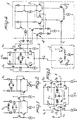
- L and C respectively indicate the coil and the capacitor which constitute the external resonating circuit, which has a terminal voltage equal to V T sin(wt).
- the integrated circuit provided for driving the external resonating circuit comprises a differential stage which includes a pair of transistors T3 and T4, the collectors whereof are connected to the power supply V CC by means of respective resistors R.
- the collectors of the two transistors T3 and T4 are furthermore connected to the two output bump contacts for connection to the external resonating circuit.
- the feedback circuits T1,D1 and T2,D2 ensure that the collector of the transistors T3 and T4 never drops below the voltage of the respective bases and that therefore these transistors never saturate.
- the circuit is completed by the current generator I O , connected to the joined emitters of the transistors T3 and T4, and the current generators I, which are connected to the bases of the transistors T3 and T4.
- Two capacitors C s are furthermore connected with one terminal to the collector of the transistors T3 and T4. According to the invention, a fraction K of the potential difference which occurs between the two output terminals (and therefore occurs across the terminals of the external resonating circuit) is applied to the other two terminals of the capacitors C s .
- i T G T ⁇ V T cos( ⁇ t)
- G T the load impedance given by:
- V x (K - 1) V T 2 sin ( ⁇ t)
- the oscillation frequency assumes the values comprised between 38.3 megahertz and 39.5 megahertz for K variable between -1 and 1.
- the factor K can be obtained by means of a linear multiplier, for example provided as a Gilbert multiplier.
- a linear multiplier for example provided as a Gilbert multiplier.
- the complete solution with the Gilbert multiplier is thus shown in figure 4, wherein it is possible to identify, besides the diagram already shown in figure 3, the block 1, which indeed constitutes the linear multiplier (which is not described in detail, since it is well-known, and substantially comprises a Gilbert multiplier 3 and a voltage/current converter 4 interposed between the actual multiplier 3 and the points A and B) and a bias current adjustment block 2.
- V c indicates the external oscillation frequency control voltage.
- the block 2 which is substantially constituted by a differential stage formed by the transistors T5 and T6, which have emitter resistors and respectively receive, on their bases, a reference voltage V ref and the external control voltage V c , is advantageously provided in order to keep the peak-to-peak value of the oscillation constant.
- the load impedance G T in fact depends on the frequency and more precisely the absolute value of the load impedance G T decreases as the operating frequency decreases.
- variable oscillator has in fact been provided which can be easily integrated (the capacity values required for C s are widely compatible with those which can be obtained by integrated capacitors) and is such as to be extensively independent of process parameter variations and of temperature variations.
- the set frequency depends in fact only on the external components (L and C), on the integrated capacitors C s (which can be provided with good precision) and on the factor K, which can be controlled satisfactorily since it is set by means of a linear multiplier.
- Temperature sensitivity is of the following order of magnitude: 1 f o ⁇ f o ⁇ T ⁇ 50 /ppm (parts per million)
- Relative sensitivity is of the following order of magnitude: 1 f o ⁇ f o ⁇ C s ⁇ 30 ppm/spread percentage point
- the invention is furthermore conceptually simple and highly reliable.
Landscapes
- Inductance-Capacitance Distribution Constants And Capacitance-Resistance Oscillators (AREA)
- Stabilization Of Oscillater, Synchronisation, Frequency Synthesizers (AREA)
Claims (6)
- Spannungsgesteuerter variabler Oszillator, insbesondere für Phasenregelkreise, mit einer Differenzstufe, gebildet durch ein Paar Transistoren (T₃ und T₄), welche Kollektoranschlüsse (A, B) haben, die zum Anschluß an einen Resonanzkreis (LC) geeignete Anschlüsse bilden,
dadurch gekennzeichnet, daß er einen Spannungsvervielfacher (1) umfaßt, welcher eine Spannung erzeugt, die proportional zu einer externen Oszillationsfrequenz-Steuerspannung (Vc) und zu der Anschluß ist, welche an den Ausgangsanschlüssen des Resonanzkreises anliegt, wobei ein Eingang (4) des Spannungsvervielfachers an wenigstens einen der Ausgangsanschlüsse (A, B) und der Ausgang des Vervielfachers, der eine in Phase mit dem entsprechenden Eingangssignal liegende Ausgangsspannung abgibt, an wenigstens einen der Ausgangsanschlüsse (A, B) durch einen Kondensator (Cs) angeschlossen ist, über welchen der Spannungsabfall (VX) zwischen der Anschlußspannung und der durch den Spannungsvervielfacher erzeugten Spannung anliegt. - Oszillator nach Anspruch 1,
dadurch gekennzeichnet, daß der Spannungsvervielfacher (1) einen Gilbert-Multiplizierer (3) beinhaltet. - Oszillator nach einem der vorstehenden Ansprüchen,
gekennzeichnet durch ein Paar Kondensatoren (Cs), von denen jeder mit einem Anschluß an einen entsprechenden Ausgangsanschluß und mit dem anderen Anschluß an die entsprechenden Anschlüsse des Gilbert-Multiplizierers angeschlossen ist. - Oszillator nach einem oder mehreren der vorstehenden Ansprüche,
gekennzeichnet durch ein Paar Rückkopplungsschaltungen (T₁, D₁ und T₂, D₂), die zwischen dem Kollektoranschluß eines der Transistoren (T₃ oder T₄) der Differenzstufe und dem Basisanschluß des anderen Transistors (T₄ oder T₃) angeordnet sind. - Oszillator nach einem oder mehreren der vorstehenden Ansprüche,
gekennzeichnet durch eine veränderbare Stromquelle (2), welche an die Emitteranschlüsse der Transistoren (T₃ und T₄) der Differenzstufe angeschlossen ist, um den Ruhestrom der Differenzstufe zu verändern, wenn sich die Betriebsfrequenz des Resonanzkreises verändert. - Oszillator nach einem oder mehreren der vorstehenden Ansprüche,
dadurch gekennzeichnet, daß die veränderbare Stromquelle (2) eine Differenzstufe umfaßt, welche an ihren Eingängen eine Referenzspannung (Vref) und die Frequenzsteuerspannung (Vc) des Oszillators erhält.
Applications Claiming Priority (2)
| Application Number | Priority Date | Filing Date | Title |
|---|---|---|---|
| IT2146289 | 1989-08-07 | ||
| IT8921462A IT1230536B (it) | 1989-08-07 | 1989-08-07 | Oscillatore variabile controllato in tensione, in particolare per circuiti ad aggancio di fase. |
Publications (3)
| Publication Number | Publication Date |
|---|---|
| EP0412435A2 EP0412435A2 (de) | 1991-02-13 |
| EP0412435A3 EP0412435A3 (en) | 1991-04-17 |
| EP0412435B1 true EP0412435B1 (de) | 1995-06-14 |
Family
ID=11182159
Family Applications (1)
| Application Number | Title | Priority Date | Filing Date |
|---|---|---|---|
| EP90114831A Expired - Lifetime EP0412435B1 (de) | 1989-08-07 | 1990-08-02 | Spannungsgesteuerter variabler Oszillator, insbesondere für einen Phasenregelkreis |
Country Status (5)
| Country | Link |
|---|---|
| US (1) | US5034706A (de) |
| EP (1) | EP0412435B1 (de) |
| JP (1) | JPH0376316A (de) |
| DE (1) | DE69020067T2 (de) |
| IT (1) | IT1230536B (de) |
Families Citing this family (11)
| Publication number | Priority date | Publication date | Assignee | Title |
|---|---|---|---|---|
| GB9027738D0 (en) * | 1990-12-20 | 1991-02-13 | Stc Plc | Crystal oscillator |
| JP3211999B2 (ja) * | 1992-06-26 | 2001-09-25 | キヤノン株式会社 | 光磁気記録装置 |
| US5357220A (en) * | 1993-01-21 | 1994-10-18 | Gennum Corporation | Emitter-coupled oscillator with differential switching control |
| US5311149A (en) * | 1993-03-12 | 1994-05-10 | Trimble Navigation Limited | Integrated phase locked loop local oscillator |
| GB9418526D0 (en) * | 1994-09-14 | 1994-11-02 | Plessey Semiconductors Ltd | Semiconductor circuit arrangements |
| FR2730363A1 (fr) * | 1995-02-08 | 1996-08-09 | Philips Electronics Nv | Amplificateur a gain eleve en hautes frequences et oscillateur a circuit resonant muni d'un tel amplificateur |
| US5635863A (en) * | 1995-05-25 | 1997-06-03 | Vtc, Inc. | Programmable phase comparator |
| US6169459B1 (en) * | 1999-05-19 | 2001-01-02 | Sandia Corporation | Active-bridge oscillator |
| US6278338B1 (en) * | 2000-05-01 | 2001-08-21 | Silicon Wave Inc. | Crystal oscillator with peak detector amplitude control |
| EP1276226B1 (de) * | 2001-06-26 | 2008-07-30 | Nxp B.V. | Schaltung zur Erzeugung einer negativen, relativ frequenzunabhängigen Konduktanz- |
| US7170332B2 (en) * | 2004-04-15 | 2007-01-30 | Analog Devices, Inc. | Reference signal generators |
Family Cites Families (5)
| Publication number | Priority date | Publication date | Assignee | Title |
|---|---|---|---|---|
| DE1269643B (de) * | 1967-07-22 | 1968-06-06 | Telefunken Patent | Schaltungsanordnung zur Synchronisierung quarzstabilisierter Oszillatoren in Traegerfrequenzsystemen mit unterdruecktem Traeger |
| US3963996A (en) * | 1974-09-05 | 1976-06-15 | Zenith Radio Corporation | Oscillation system for integrated circuit |
| US4243953A (en) * | 1979-02-16 | 1981-01-06 | Rca Corporation | Voltage controlled oscillator presenting high impedance to parallel resonant tank circuit |
| US4286235A (en) * | 1979-06-25 | 1981-08-25 | Rca Corporation | VFO having plural feedback loops |
| US4524389A (en) * | 1981-11-09 | 1985-06-18 | Matsushita Electric Industrial Co., Ltd. | Synchronous video detector circuit using phase-locked loop |
-
1989
- 1989-08-07 IT IT8921462A patent/IT1230536B/it active
-
1990
- 1990-07-30 US US07/559,799 patent/US5034706A/en not_active Expired - Lifetime
- 1990-08-02 DE DE69020067T patent/DE69020067T2/de not_active Expired - Fee Related
- 1990-08-02 EP EP90114831A patent/EP0412435B1/de not_active Expired - Lifetime
- 1990-08-03 JP JP2207491A patent/JPH0376316A/ja active Pending
Also Published As
| Publication number | Publication date |
|---|---|
| IT8921462A0 (it) | 1989-08-07 |
| EP0412435A2 (de) | 1991-02-13 |
| EP0412435A3 (en) | 1991-04-17 |
| US5034706A (en) | 1991-07-23 |
| IT1230536B (it) | 1991-10-28 |
| DE69020067T2 (de) | 1996-02-01 |
| DE69020067D1 (de) | 1995-07-20 |
| JPH0376316A (ja) | 1991-04-02 |
Similar Documents
| Publication | Publication Date | Title |
|---|---|---|
| EP0412435B1 (de) | Spannungsgesteuerter variabler Oszillator, insbesondere für einen Phasenregelkreis | |
| US4581593A (en) | Variable frequency oscillating circuit | |
| US5708394A (en) | Bridge-stabilized oscillator circuit and method | |
| JPH05243845A (ja) | 電圧制御発振回路 | |
| US4990872A (en) | Variable reactance circuit producing negative to positive varying reactance | |
| JPH01106525A (ja) | 周波数発生回路装置 | |
| US4595887A (en) | Voltage controlled oscillator suited for being formed in an integrated circuit | |
| US5406631A (en) | Stereo signal demodulator circuit and stereo signal demodulator using the same | |
| JPH07263957A (ja) | 電圧制御発振器 | |
| US4346351A (en) | High frequency voltage-controlled oscillator | |
| US5444422A (en) | Low phase noise high frequency integrated oscillator with minimum pins | |
| US6492879B2 (en) | Voltage-controlled oscillator | |
| US4517533A (en) | Integrated crystal VCO | |
| JP2002016442A (ja) | Fm信号発振回路及び変調レベル補正方法 | |
| US4914406A (en) | Voltage controlled oscillator free from free-run oscillating frequency adjustment | |
| JPH0332088Y2 (de) | ||
| JPS6021602A (ja) | 可変周波数水晶発振回路 | |
| KR880000364Y1 (ko) | 바이어스 전류에 의한 위상 고정루우프 주파수 변조회로 | |
| JP2602313B2 (ja) | 発振回路 | |
| JP2903934B2 (ja) | 発振回路と、この発振回路を用いたbsチューナ | |
| JPH0317454Y2 (de) | ||
| JPH08191214A (ja) | 電圧制御発振器 | |
| JPH0516722Y2 (de) | ||
| JPS62290214A (ja) | 位相同期発振器 | |
| SU944068A1 (ru) | Генератор,управл емый напр жением |
Legal Events
| Date | Code | Title | Description |
|---|---|---|---|
| PUAI | Public reference made under article 153(3) epc to a published international application that has entered the european phase |
Free format text: ORIGINAL CODE: 0009012 |
|
| AK | Designated contracting states |
Kind code of ref document: A2 Designated state(s): DE FR GB NL SE |
|
| PUAL | Search report despatched |
Free format text: ORIGINAL CODE: 0009013 |
|
| AK | Designated contracting states |
Kind code of ref document: A3 Designated state(s): DE FR GB NL SE |
|
| 17P | Request for examination filed |
Effective date: 19910726 |
|
| 17Q | First examination report despatched |
Effective date: 19930714 |
|
| GRAA | (expected) grant |
Free format text: ORIGINAL CODE: 0009210 |
|
| AK | Designated contracting states |
Kind code of ref document: B1 Designated state(s): DE FR GB NL SE |
|
| REF | Corresponds to: |
Ref document number: 69020067 Country of ref document: DE Date of ref document: 19950720 |
|
| PG25 | Lapsed in a contracting state [announced via postgrant information from national office to epo] |
Ref country code: SE Effective date: 19950914 |
|
| ET | Fr: translation filed | ||
| PLBE | No opposition filed within time limit |
Free format text: ORIGINAL CODE: 0009261 |
|
| STAA | Information on the status of an ep patent application or granted ep patent |
Free format text: STATUS: NO OPPOSITION FILED WITHIN TIME LIMIT |
|
| 26N | No opposition filed | ||
| REG | Reference to a national code |
Ref country code: FR Ref legal event code: D6 |
|
| REG | Reference to a national code |
Ref country code: GB Ref legal event code: IF02 |
|
| PGFP | Annual fee paid to national office [announced via postgrant information from national office to epo] |
Ref country code: GB Payment date: 20020731 Year of fee payment: 13 |
|
| PGFP | Annual fee paid to national office [announced via postgrant information from national office to epo] |
Ref country code: DE Payment date: 20020807 Year of fee payment: 13 |
|
| PGFP | Annual fee paid to national office [announced via postgrant information from national office to epo] |
Ref country code: FR Payment date: 20020808 Year of fee payment: 13 |
|
| PG25 | Lapsed in a contracting state [announced via postgrant information from national office to epo] |
Ref country code: GB Free format text: LAPSE BECAUSE OF NON-PAYMENT OF DUE FEES Effective date: 20030802 |
|
| PG25 | Lapsed in a contracting state [announced via postgrant information from national office to epo] |
Ref country code: DE Free format text: LAPSE BECAUSE OF NON-PAYMENT OF DUE FEES Effective date: 20040302 |
|
| GBPC | Gb: european patent ceased through non-payment of renewal fee |
Effective date: 20030802 |
|
| PG25 | Lapsed in a contracting state [announced via postgrant information from national office to epo] |
Ref country code: FR Free format text: LAPSE BECAUSE OF NON-PAYMENT OF DUE FEES Effective date: 20040430 |
|
| REG | Reference to a national code |
Ref country code: FR Ref legal event code: ST |
|
| PGFP | Annual fee paid to national office [announced via postgrant information from national office to epo] |
Ref country code: NL Payment date: 20090724 Year of fee payment: 20 |
|
| REG | Reference to a national code |
Ref country code: NL Ref legal event code: V4 Effective date: 20100802 |
|
| PG25 | Lapsed in a contracting state [announced via postgrant information from national office to epo] |
Ref country code: NL Free format text: LAPSE BECAUSE OF EXPIRATION OF PROTECTION Effective date: 20100802 |