EP0410743B1 - Graphisches Anzeigesystem mit einem geteilten seriellen Register - Google Patents
Graphisches Anzeigesystem mit einem geteilten seriellen Register Download PDFInfo
- Publication number
- EP0410743B1 EP0410743B1 EP90308184A EP90308184A EP0410743B1 EP 0410743 B1 EP0410743 B1 EP 0410743B1 EP 90308184 A EP90308184 A EP 90308184A EP 90308184 A EP90308184 A EP 90308184A EP 0410743 B1 EP0410743 B1 EP 0410743B1
- Authority
- EP
- European Patent Office
- Prior art keywords
- register
- data
- memory
- row
- split
- Prior art date
- Legal status (The legal status is an assumption and is not a legal conclusion. Google has not performed a legal analysis and makes no representation as to the accuracy of the status listed.)
- Expired - Lifetime
Links
Images


Classifications
-
- G—PHYSICS
- G06—COMPUTING; CALCULATING OR COUNTING
- G06F—ELECTRIC DIGITAL DATA PROCESSING
- G06F3/00—Input arrangements for transferring data to be processed into a form capable of being handled by the computer; Output arrangements for transferring data from processing unit to output unit, e.g. interface arrangements
- G06F3/14—Digital output to display device ; Cooperation and interconnection of the display device with other functional units
- G06F3/153—Digital output to display device ; Cooperation and interconnection of the display device with other functional units using cathode-ray tubes
-
- G—PHYSICS
- G09—EDUCATION; CRYPTOGRAPHY; DISPLAY; ADVERTISING; SEALS
- G09G—ARRANGEMENTS OR CIRCUITS FOR CONTROL OF INDICATING DEVICES USING STATIC MEANS TO PRESENT VARIABLE INFORMATION
- G09G5/00—Control arrangements or circuits for visual indicators common to cathode-ray tube indicators and other visual indicators
- G09G5/36—Control arrangements or circuits for visual indicators common to cathode-ray tube indicators and other visual indicators characterised by the display of a graphic pattern, e.g. using an all-points-addressable [APA] memory
- G09G5/39—Control of the bit-mapped memory
- G09G5/395—Arrangements specially adapted for transferring the contents of the bit-mapped memory to the screen
Definitions
- This invention relates to a graphics display system and more particularly to such a system using a split-serial register for controlling data transfer to the graphic display.
- the number of pixels on a screen and thus the number of points which must be read from the display memory is significant. Also the amount of display memory is critical for economical utilization of any system.
- the display memory holds a line of data which must be read to the screen in a short interval of time. This is accomplished by arranging the memory with a serial register which will remove a full line of data from the memory and transfer that line to the screen.
- VRAMS which have 512 bits in a row length. These memories have several planes, usually four each, and are arranged to fill the bus for each memory read cycle. Thus, for a 32 bit bus, 8 VRAMS, each having 4 planes, could be used.
- serial register for each plane of each memory would be 512 bits long, thereby transferring 16384 bits to the display for each memory-to-serial register read cycle.
- These 16384 bits represent data for 2048 display pixels, assuming each pixel contains 8 bits.
- each scan line only requires 1280 pixels.
- This memory is difficult to use for other purposes and thus, is effectively wasted.
- EP-A-0,245,564 there is disclosed a bit map memory connected to four shift registers which can be loaded in parallel with pixel information from the memory. At least one shift register is clocked at a suitable rate to feed data for display to a video display device. The other shift registers are clocked at different rates to suit different peripheral units. Masks can be inserted in the paths from the bit map memory to the shift registers for selectively removing certain of the pixel bits.
- serial register graphic reloading system which allows for continuously filling the pixels on a line of a graphics display screen, while being independent of the screen line length and which conserves memory and register space.
- a graphics processing system comprising:
- a method of producing a graphics display on a graphics presentation medium using a register split into two portions (A,B), each portion being operable for serially transferring data from that portion while allowing the other portion to be reloaded with data at the same time characterised in that the method comprises the steps of:
- a split-serial register is utilized in a graphic processing system to control screen transfer information such that information is shifted continuously from the shift registers during each line output, thereby providing uninterrupted data flow to the screen.
- the system allows for mid-line reloading without detection by a viewer.
- Both halves of the serial register are adapted to be loaded during the horizontal blanking (interline flyback) screen refresh cycle at the same time the column address of the beginning point of the line is provided to an address register.
- the data is outputted serially from one half of the data register to the screen, beginning from the bit corresponding to the column address.
- the address of the serial register then logically counts (in conjunction with the shifting of data from the register) from the starting address up to all 1's and then rolls over to all 0's. At the zero point shifting of data automatically begins from the other half of the serial register. This then allows the currently unused half of the register to be available for receiving the data corresponding to the next portion of the screen information.
- This problem is solved by including a split serial register refresh cycle where the address of the next half row is generated immediately following the ordinary horizontal blanking screen refresh. This is the same type of cycle used for the midline reload screen refresh cycles and only loads half of each of the serial registers.
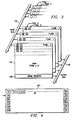
- FIGURE 1 illustrates a block diagram of graphics computer system 100 which is constructed in accordance with the principles of the present invention.
- Graphics computer system 100 includes host processing system 110, graphics processor 120, memory 130, shift register 140, video palette 150, digital to video converter 160, and video display 170.
- Host processing system 110 provides the major computational capacity for the graphics computer system 100.
- Host processing system 110 preferably includes at least one microprocessor, read only memory, random access memory and assorted peripheral devices for forming a complete computer system.
- Host processing system 110 preferably also includes some form of input device, such as a keyboard or a mouse, and some form of long term storage device such as a disk drive.
- input device such as a keyboard or a mouse
- some form of long term storage device such as a disk drive.
- the details of the construction of host processing system 110 are conventional in nature and known in the art, therefore the present application will not further detail this element.
- the essential feature of host processing system 110 is that host processing system 110 determines the content of the visual display to be presented to the user.
- Graphics processor 120 provides the major data manipulation in accordance with the present invention to generate the particular video display presented to the user.
- Graphics processor 120 is bidirectionally coupled to host processing system 110 via host bus 115.
- graphics processor 120 operates as an independent data processor from host processing system 110; however, it is expected that graphics processor 120 is responsive to requests from host processing system 110 via host bus 115.
- Graphics processor 120 further communicates with memory 130, and video palette 150 via video memory bus 122.
- Graphics processor 120 controls the data stored within video RAM 132 via video memory bus 122.
- graphics processor 120 may be controlled by programs stored in either video RAM 132 or read only memory 134.
- Read only memory 134 may additionally include various types of graphic image data, such as alphanumeric characters in one or more font styles and frequently used icons.
- graphics processor 120 controls the data stored within video palette 150.
- graphics processor 120 controls digital to video converter 160 via video control bus 124.
- Graphics processor 120 may control the line length and the number of lines per frame of the video image presented to the user by control of digital to video converter 160 via video control bus 124.
- Video memory 130 includes video RAM 132 which is bidirectionally coupled to graphics processor 120 via video memory bus 122 and read only memory 134.
- video RAM 134 includes the bit mapped graphics data which controls the video image presented to the user. This video data may be manipulated by graphics processor 120 via video memory bus 122.
- the video data corresponding to the current display screen is output from video RAM 132 via video output bus 136.
- the data from video output bus 136 corresponds to the picture element to be presented to the user.
- video RAM 132 is formed of a plurality of TMS44251 256KX4 dynamic random access integrated circuits available from Texas Instruments Corporation, the assignee of the present application.
- the TMS44251 integrated circuit includes dual ports, enabling display refresh and display update to occur without interference.
- Shift register 140 receives the video data from video RAM 132 and assembles it into a display bit stream.
- this memory consists of a bank of several separate random access memory integrated circuits. The output of each of these integrated circuits is typically only one or four bits wide. Therefore, it is necessary to assemble data from a plurality of these circuits in order to obtain a sufficiently high data output rate to specify the image to be presented to the user.
- Shift register 140 is loaded in parallel from video output bus 136. This data is output in series on line 145. Thus, shift register 140 assembles a display bit stream which provides video data at a rate high enough to specify the individual dots within the raster scanned video display.
- Video palette 150 receives the high speed video data from shift register 140 via bus 145. Video palette 150 also receives data from graphics processor 120 via video memory bus 122. Video palette 150 converts the data received on bus 145 into a video level output on bus 155. This conversion is achieved by means of a look-up table which is specified by graphics processor 120 via video memory bus 122. The output of video palette 150 may comprise color hue and saturation for each picture element or may comprise red, green and blue primary color levels for each pixel. The table of conversion from the code stored within video memory 132 and the digital levels output via bus 155 is controlled from graphics processor 120 via video memory bus 122.
- Digital to video converter 160 receives the digital video information from video palette 150 via bus 155.
- Digital to video converter 160 is controlled by graphics processor 120 via video control bus 134.
- Digital to video converter 160 serves to convert the digital output of video palette 150 into the desired analog levels for application to video display 170 via video output 165.
- Digital to video converter 160 is controlled for a specification of the number of pixels per horizontal line and the number of lines per frame, for example, by graphics processor 120 via video controller bus 124.
- Data within graphics processor 120 controls the generation of the synchronization and blanking signals and the retrace signals by digital to video converter 160. These portions of the video signal are not specified by the data stored within video memory 132, but rather form the control signals necessary for specification of the desired video output.
- video display 170 receives the video output from digital to video converter 160 via video output line 165.
- Video display 170 generates the specified video image for viewing by the operator of graphics computer system 100.
- video palette 150, digital to video converter 160 and video display 170 may operate in accordance to two major video techniques. In the first, the video data is specified in terms of color hue and saturation for each individual pixel. In the other technique, the individual primary color levels of red, blue and green are specified for each individual pixel. Upon determination of the design choice of which of these major techniques to be employed, video palette 150, digital to converter 160 and video display 170 must be constructed to be compatible to this technique. However, the principles of the present invention in regard to the operation of graphics processor 120 are unchanged regardless of the particular design choice of video technique.
- FIGURE 2 illustrates graphics processor 120 in further detail.
- Graphics processor 120 includes central processing unit 200, special graphics hardware 210, register files 220, instruction cache 230, host interface 240, memory interface 250, input/output registers 260 and video display controller 270.
- Central processing unit 200 includes the capacity to do general purpose data processing including a number of arithmetic and logic operations normally included in a general purpose central processing unit. In addition, central processing unit 200 controls a number of special purpose graphics instructions, either alone or in conjunction with special graphics hardware 210.
- Graphics processor 120 includes a major bus 205 which is connected to most parts of graphics processor 120 including the central processing unit 200.
- Central processing unit 200 is bidirectionally coupled to a set of register files, including a number of data registers, via bidirectional register bus 202.
- Register files 220 serve as the depository of the immediately accessible data used by central processing unit 200.
- register files 220 include, in addition to general purpose registers which may be employed by central processing unit 200, a number of data registers which are employed to store implied operands for graphics instructions.
- Central processing unit 200 is connected to instruction cache 230 via instruction cache bus 204.
- Instruction cache 230 is further coupled to bus 205 and may be loaded with instruction words from video memory 132 (FIGURE 1) via video memory bus 122 and memory interface 250.
- the purpose of instruction cache 230 is to speed up the execution of certain functions of central processing unit 200.
- a repetitive function or function that is used often within a particular portion of the program executed by central processing unit 200 may be stored within instruction cache 230.
- Access to instruction cache 230 via instruction cache bus 204 is much faster than access to video memory 130.
- the program executed by central processing unit 200 may be speeded up by preliminarily loading the repeated or often used sequences of instructions within instruction cache 230. Then these instructions may be executed more rapidly because they may be fetched more rapidly.
- Instruction cache 230 need not always contain the same sets of instructions, but may be loaded with a particular set of instructions which will be often used within a particular portion of the program executed by central processing unit 200.
- Host interface 240 is coupled to central processing unit 200 via host interface bus 206. Host interface 240 is further connected to host processing system 110 (FIGURE 1) via host system bus 115. Host interface 240 serves to control the communication between host processing system 110 and graphics processor 120. Host interface 240 controls the timing of data transfer between host processing system 110 and graphics processor 120. In this regard, host interface 240 enables either host processing system 110 to interrupt graphics processor 120 or vice versa enabling graphics processor 120 to interrupt host processing system 110. In addition, host interface 240 is coupled to major bus 205 enabling host processing system 110 to control directly the data stored within memory 130. Typically, host interface 240 would communicate graphics requests from host processing system 110 to graphics processor 120, enabling the host system to specify the type of display to be generated by video display 170 and causing graphic processor 120 to perform a desired graphic function.
- Central processing unit 200 is coupled to special graphics hardware 210 via graphics hardware bus 208.
- Special graphics hardware 210 is further connected to major bus 205.
- Special graphics hardware 210 operates in conjunction with central processing unit 200 to perform special graphic processing operations.
- Central processing unit 200 in addition to its function of providing general purpose data processing, controls the application of the special graphics hardware 210 in order to perform special purpose graphics instructions.
- These special purpose graphics instructions concern the manipulation of data within the bit mapped portion of video RAM 132.
- Special graphic hardware 210 operates under the control of central processing unit 200 to enable particular advantageous data manipulations regarding the data within video RAM 132.
- Memory interface 250 is coupled to bus 205 and further coupled to video memory bus 122.
- Memory interface 250 serves to control the communication of data and instructions between graphics processor 120 and memory 130.
- Memory 130 includes both the bit mapped data to be displayed via video display 170 and instructions and data necessary for the control of the operation of graphics processor 120. These functions include control of the timing of memory access, and control of data and memory multiplexing.
- video memory bus 122 includes multiplexed address and data information.
- Memory interface 250 enables graphics processor 120 to provide the proper output on video memory bus 122 at the appropriate time for access to memory 130.
- Graphics processor 120 lastly includes input/output registers 260 and video display controller 270.
- Input/output registers 260 are bidirectionally coupled to bus 205 to enable reading and writing within these registers.
- Input/output registers 260 are preferably within the ordinary memory space of central processing unit 200.
- Input/output registers 260 include data which specifies the control parameters of video display controller 270.
- video display controller 270 generates the signals on video control bus 124 for the desired control of digital to video converter 160.
- Data within input/output registers 260 includes data for specifying the number of pixels per horizontal line, the horizontal synchronization and blanking intervals, the number of horizontal lines per frame and the vertical synchronization and blanking intervals.
- Input/output registers 260 may also include data which specifies the type of frame interlace and specifies other types of video control functions. Lastly, input/output registers 260 is a depository for other specific kinds of input and output parameters which will be more fully detailed below.
- Graphics processor 120 operates in two differing address modes to address memory 130. These two address modes are x y addressing and linear addressing. Because the graphics processor 120 operates on both bit mapped graphic data and upon conventional data and instructions, different portions of the memory 130 may be accessed most conveniently via differing addressing modes. Regardless of the particular addressing mode selected, memory interface 250 generates the proper physical address for the appropriate data to be accessed.
- liner addressing the start address of a field is formed of a single multibit linear address. The field size is determined by data within a status register within central processing unit 200. In x y addressing the start address is a pair of x and y coordinate values. The field size is equal to the size of a pixel, that is the number of bits required to specify the particular data at a particular pixel.
- FIGURE 3 a brief discussion of the memory structure of a typical graphics memory system is in order before progressing to the actual detailed description of the functioning of the embodiment of this invention. While there are many memory structures and system which could be used, it has become typical to use a structure, such as shown in FIGURE 3, which uses eight VRAM memories 130 in an array. Each VRAM memory, or unit, having four sections, or planes, 0, 1, 2 and 3. The construction of each plane is such that a single data lead is used to write information to that plane. In a system which uses a 32 bit data bus, such as data bus 122, there would be 8 VRAM memories (two of which are shown in FIGURE 3) each VRAM memory having four data leads connected to the input data bus.
- VRAM memory 130 would have its four data leads connected to data bus leads 0, 1, 2, 3 respectively.
- the next VRAM memory would have its four leads 0, 1, 2, 3 connected to data bus leads 4, 5, 6, 7, respectively. This continues for the remaining six VRAM's such that the last VRAM has its leads connected to leads 28, 29, 30 31 of bus 122.
- the memories are arranged such that the pixel information for the graphics display is stored serially across the planes in the same row. Assuming a four bit per pixel system, then the bits for each pixel are stored in a separate VRAM memory. In such a situation, pixel 0 would be in the first VRAM and pixel 1 would be in the second VRAM. The pixel storage for pixels 2 through 7 are not shown. The pixel information for pixel 8 then would be stored in the first VRAM, still in row 0 but in column 2 thereof. The reason for this arrangement of pixel information will be more fully appreciated from an understanding of how information is retrieved from the memory.
- each VRAM plane has a serial register 140 for shifting out information from a row of memory.
- the outputs from these registers are connected to bus 145 in the same manner as the data input leads are connected to the input bus.
- data from a row of memory say row 0, would be moved into register 140. This would occur for each plane of the eight memory array.
- bus 145 At an instant of time the first bit in each shift register would be on the bus. Thus, assuming row 0 is being outputted to the bus, the bus would have on it's lead 0 the row 0, bit A0 (plane 0) of memory 130. Bus 145 lead 1 would have on it row 0, bit A0 (plane 1), while lead 2 would have row 0, bit A0 (plane 2) and lead 3 would have on it row 0, bit A0 (plane 3). These bits would be followed by the bits from the next VRAM. Thus, at a first instant of time, data bus 145 would have on it the four bits forming pixel 0 followed by the four bits forming pixel 1, followed by the four bits forming pixel 2.
- bit information per pixel is 4 bits. If the pixel information were to be, say 8 bits, then two VRAMs would have to be used per pixel. This would change the bit patterns somewhat. Also, it should be noted that memory sizes and structures continue to vary and the size and structure shown are only for illustrative purposes and this invention can be used with many different memory configurations and with different pixel sizes.
- the serial register for each plane of each memory would be 512 bits long thereby transferring 16384 bits to the display for each memory-to-serial register read cycle.
- These 16384 bits represent data for 2048 display pixels, assuming each pixel contains 8 bits.
- each scan line only requires 1280 pixels.
- This memory as will become clearer as we progress herein, is difficult to use for other purpose and thus is effectively wasted.
- serial output register has been split in half and each half is used to output data from the VRAM. While it is understood that 32 shift registers are used, our discussion will focus on only one plane of the memory with the understanding that all planes work in the same manner.
- the two halves of the register are known as half A and half B.
- the object of the serial register is to take from memory an entire row of screen memory and present that row to the screen pixel-by-pixel in a smooth, even flow.
- FIGURE 4 there is shown a graphics screen 401 having 39 pixels across its face and several rows of pixels down.
- the numbers used here are for illustration only and bear no resemblance to the number of pixels, typically 1280, across the face of an actual graphics screen. The actual numbers are so high that the operation of the invention will become burdensome if the example cited were to use numbers approaching those actually found in typical systems.
- FIGURE 5 which is to follow and system arrangements using real numbers will serve only to obscure the discussion.
- memory 501 used for discussion purposes has less column capacity (16), in terms of pixels, than does screen 401. In practice, this would typically be the reverse.
- memory 501 is shown with four planes. It will be assumed that each pixel has 4 bits. For our purposes herein we will also assume that only two such memory units are being used, one containing even pixels and one (not shown) containing odd pixels. This would result in use of only 8 bits, or leads, of the bus, four bits from each memory unit. We will also assume that the memory has only 16 columns, labeled 0 through 15. Thus, row 0 is labeled A0 through A15 while row 1 is labeled B0 through B15. If we further simplify our discussion by restricting the discussion to the memory unit containing only the even pixels, then it can be thought of that bit A0 represents data for pixel 0 and bit A1 represents data for pixel 2. This follows since the A0 bit in the unseen second VRAM would contain information of pixel 1.
- Control of the serial register is such that when the first half of the register is finished sending data it can be cleared and reloaded so that while the bits are being sent from the second half of the register new data bits can be loaded in the first half. If, in fact, the bits to be sent first were to be in the second half of the register, the B half, then the A half would have to be reloaded immediately. This fact also must be determined. These determinations are made from the address information provided to the memory and are dependent upon the bit positions and number of bits necessary to specify an address.
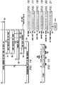
- FIGURE 9 shows a 10 bit row and column address preceded by 3 bank select bits and 5 miscellaneous address bits.
- FIGURE 10 shows 8 bit row and column address bits preceded only by the miscellaneous address bits.
- FIGURE 11 shows a mask for use with the FIGURE 9 address configuration while FIGURE 12 shows a mask for use with the FIGURE 10 configuration.
- FIGURE 13 shows the mask that will be used by the system that we are discussing, namely three tap point bits (16 possible columns, 8 in each half-shift register) preceded by two bank select bits. These bits were added for the sake of discussion.
- FIGURE 14 there is a diagram laying out how these masks are to be used.
- FIGURES 15 through 20 illustrate our example.
- FIGURE 15 shows the row and column address bits for row 1, column 4 of the memory which, it will be recalled, is where the first pixel 40 for the selected screen row resides.
- the bit word depicted in FIGURE 15 also has other address bits 0-4, and bank bits 5-6.
- the tap point bits are loaded into tap point register 91.
- the tap point is defined as the bit position in the register which will be read to the bus first. This tap point is calculated from the address information of FIGURE 15. In our example, the first five bits of the address (0-4) can be ignored since they would be constant for all configurations as a design matter.
- the next thirteen bits of the address are transferred to tap register 91, FIGURE 16.
- mask 93 which was created for our example system (FIGURE 13), is copied into mask shift register 92.
- This mask serves to adjust the tap point for the possible variation of bank select bits. In our example there were two such bits and thus the first two bits of the mask are 0's.
- a clock then shifts registers 92 and 91 to the right until a 1 appears in the right most position of shift register 92 (FIGURE 19). This operation serves to remove the bank bits from the tap point, which then becomes 100 as seen from register 91, FIGURE 20.
- tap point counter 94 (FIGURE 21).
- the shifted mask 92 (FIGURE 19 determines how many bits of counter 94 are significant.)
- This tap point which is defined as the position in the serial register to be read first to the data bus, can be seen in FIGURE 6, corresponding to pixel 40 controlled by bit B4 in half-register A.
- Register A is selected, as apposed to register B, since the left most column bit equals 0 in FIGURE 15. Had the left most position of the column address contained a 1, the B half of the serial register would have been selected.
- clock 2001 operating in conjunction with the memory shift clock, serves to increment the tap point shift register in conjunction with data being read from the serial register.
- the tap point register contains all 111's it signifies that the data from position 111 of half-register A, FIGURE 6, is being read to the bus. This corresponds to pixel 46, memory bit B7.
- the tap point counter overflows to 000 as shifting begins from half-register B where memory positions B8 to B15 are in turn sent to the graphics display. Note that the register operation just described does not control the actual shifting out of data, but controls the reloading of data into the serial register.
- half-register A is cleared and information from memory positions C0 to C7, the next memory row, are loaded into half-register A.
- This alternate operation will continue until the screen reaches the end of the row, i.e. pixel 79 is sent to the screen.
- the half-row reload requires an address, which points to the 1st bit in the half row being reloaded. This addresss comes from "incrementable copy of row address", 95.
- Register 95 is loaded from register 90 when register 91 is loaded from register 90. It is then incremented at the left-most bit of the column address to point to the next half row.
- Register 93 is used to determine the bit position for the increment (the bit to the left of the left-most 1).
- register 93 When the address is output, register 93 is also used to ensure that all bits to the right of this point are zero (signifying a zero tap address, pointing to the 1st bit in the shift register). Each time the counter overflows, the address in this register is output, and then incremented.
- the tap point counter resets to 000 and, as shown in FIGURE 8, as memory bits C0 to C7 are transferred from half-register A to the bus. At this time half-register B is loaded with memory bits C8 to C15.
- the fly back interval is also reached and the registers are reset with the next full line to be read to the screen as determined by the processor. At this time the cycle repeats and a new tap point is calculated.
- the A half of the register would appear as shown in FIGURE 8 with the tap point at position C8. This would mean that the A half-register must be cleared immediately and loaded with memory bits D0 to D7 in preparation for the tap point counter again reaching 111 and rolling over so as to follow the readout of data from the first half-register A.
Claims (11)
- Verarbeitungssystem für Graphiken, umfassend:ein Medium (170) zur Darstellung von Graphiken; undein geteiltes Register (140) zum seriellen Übertragen von Daten zu dem Medium Zeile für Zeile, wobei das Register einen ersten Teil (A) und einen zweiten Teil (B) enthält und jeder Teil während der Übertragung von Daten von dem anderen Teil neu ladbar ist;dadurch gekennzeichnet, daß das Register (140) ein serielles Register ist und das System darüber hinaus ein Überwachungsregister (260) zum Verfolgen der im Register befindlichen Adressstelle der zu dem Medium übertragenen Information und eine von dem Überwachungsregister aktivierte Steuerschaltungsanordnung (120) enthält, um die serielle Übertragung von Daten nacheinander von dem ersten und dem zweiten Registerteil (A, B) durch Anlegen von Taktsignalen zu immer nur einem der Teile (A, B) zu steuern, um die Übertragung von Daten von diesem Teil zu bewirken, bis alle in diesem Teil gespeicherten Daten übertragen worden sind.
- Verarbeitungssystem für Graphiken nach Anspruch 1, bei dem das Überwachungsregister mit der im Register befindlichen Stelle der ersten Datenposition einer neuen Medienzeile geladen wird und bei dem danach das Überwachungsregister, während der Dauer der Übertragung von Daten zu der Medienzeile, bis zu einem vorher festgelegten Zählerstand inkrementiert wird.
- Verarbeitungssystem für Graphiken nach Anspruch 2, bei dem die zu übertragenden Daten in Zeilen und Spalten innerhalb eines Speichers (130) enthalten sind und bei dem die Daten von den Speicherstellen zu dem seriellen Register entweder Vollzeile für Vollzeile übertragen werden, so daß der erste und der zweite Teil des seriellen Registers Daten aus der ersten Hälfte bzw. aus der zweiten Hälfte einer gegebenen Zeile enthält, oder in halben Zeilen übertragen werden, so daß entweder der erste Teil oder der zweite Teil des Registers Daten aus der ersten Hälfte bzw. der zweiten Hälfte derselben oder verschiedener Zeilen enthält.
- Verarbeitungssystem für Graphiken nach Anspruch 3, darüber hinaus umfassend:eine angefertigte Schieberegistermaske (93); undein Schieberegister (91) für den Anfangspunkt, das Bits enthält, die die erste Datenposition repräsentieren, wobei die Bits für den Anfangspunkt durch Anpassen der Schieberegistermasken an ein vorliegendes Datenbitmuster erzeugt werden, das Zeilen- und Spaltenadressdaten in dem Speicher enthält.
- Verarbeitungssystem für Graphiken nach Anspruch 4, darüber hinaus enthaltend:
eine Inkrementierungsschaltungsanordnung (94) zur Steuerung des Überwachungsregisters in Übereinstimmung mit den Daten, die vom seriellen Register übertragen werden. - Verarbeitungssystem für Graphiken nach Anspruch 3, darüber hinaus umfassend:
ein Zeilenadressregister (Fig. 15) zur Steuerung der Datenübertragung zum seriellen Register in halben Zeilen. - Verfahren zur Herstellung einer Graphikanzeige auf einem Medium (170) zur Darstellung von Graphiken, bei dem man ein in zwei Teile (A, B) geteiltes Register (140) verwendet, wobei jeder Teil zum seriellen Übertragen von Daten von diesem Teil betrieben werden kann, während dem anderen Teil ermöglicht wird, zur gleichen Zeit mit Daten geladen zu werden, dadurch gekennzeichnet, daß das Verfahren die Schritte umfaßt:ein geteiltes Register (140) wird als ein serielles Register vorgesehen,darüber hinaus wird ein Überwachungsregister (260) vorgesehen,das Überwachungsregisters (260) wird verwendet, um die in dem geteilten Register (140) befindliche Adressstelle von Daten zu verfolgen, wenn diese zum Darstellungsmedium übertragen werden, unddie serielle Übertragung von Daten von den zwei Teilen (A, B) des geteilten Registers (140) wird, unter Bezug auf die durch das Überwachungsregister (260) verfolgte Adressstelle, nacheinander durch Anlegen von Taktsignalen zu immer nur einem der Teile (A, B) gesteuert, um die Übertragung von Daten von diesem Teil zu bewirken, bis alle in diesem Teil gespeicherten Daten übertragen worden sind.
- Verfahren nach Anspruch 7, dadurch gekennzeichnet, daß ein Speicher (130) mit Zeilen und Spalten vorgesehen wird, der die Daten zum Neuladen der Teile (A, B) des geteilten Registers (140) speichert, und dadurch, daß das Steuern der seriellen Übertragung von Daten von dem geteilten Register (140) das Annehmen einer im Speicher befindlichen Adressstelle irgendeiner Spaltenposition in irgendeiner Zeile des Speichers für die Übertragung der Daten von dieser Zeile zu dem geteilten Register (140) und das Berechnen der in dem geteilten Register befindlichen Position der ersten Datenposition einer neuen Zeile des Darstellungsmediums auf der Basis der angenommenen Adreßstelle enthält.
- Verfahren nach Anspruch 8, bei dem die Daten zum Darstellungsmedium pixelweise übertragen werden.
- Verfahren nach Anspruch 8 oder 9, bei dem der Schritt des Steuerns die Schritte enthält:Entwickeln einer Bitmaske;Erzeugen eines Anfangspunkts, der die erste Datenposition repräsentiert, wobei der Anfangspunkt durch Anpassen der Bitmaske an ein vorliegendes Datenbitmuster erzeugt wird, das die Zeilen- und Spaltenadressdaten enthält, undZählen der Positionen der Datenspeicherung auf dem geteilten Register, beginnend mit der Position innerhalb des geteilten Registers, die dem Anfangspunkt entspricht.
- Verfahren nach Anspruch 10, darüber hinaus enthaltend die Schritte:Laden eines Zählers mit den binären Werten des Anfangspunkts; undInkrementieren des Zählers zusammen mit der Übertragung von Daten von dem geteilten Register.
Applications Claiming Priority (2)
| Application Number | Priority Date | Filing Date | Title |
|---|---|---|---|
| US38756989A | 1989-07-28 | 1989-07-28 | |
| US387569 | 1989-07-28 |
Publications (3)
| Publication Number | Publication Date |
|---|---|
| EP0410743A2 EP0410743A2 (de) | 1991-01-30 |
| EP0410743A3 EP0410743A3 (en) | 1992-05-13 |
| EP0410743B1 true EP0410743B1 (de) | 1996-02-21 |
Family
ID=23530454
Family Applications (1)
| Application Number | Title | Priority Date | Filing Date |
|---|---|---|---|
| EP90308184A Expired - Lifetime EP0410743B1 (de) | 1989-07-28 | 1990-07-26 | Graphisches Anzeigesystem mit einem geteilten seriellen Register |
Country Status (5)
| Country | Link |
|---|---|
| EP (1) | EP0410743B1 (de) |
| JP (1) | JPH03164872A (de) |
| KR (1) | KR910003484A (de) |
| CN (1) | CN1049926A (de) |
| DE (1) | DE69025439T2 (de) |
Families Citing this family (3)
| Publication number | Priority date | Publication date | Assignee | Title |
|---|---|---|---|---|
| AU2003255891A1 (en) * | 2002-09-09 | 2004-03-29 | Koninklijke Philips Electronics N.V. | Driving method, driving circuit and driving apparatus for a display system |
| CN103345910B (zh) * | 2013-06-09 | 2015-11-18 | 苏州国芯科技有限公司 | 单端口调色板sram控制器及其控制方法 |
| CN206002819U (zh) | 2016-09-18 | 2017-03-08 | 京东方科技集团股份有限公司 | 阵列基板及显示器件 |
Family Cites Families (2)
| Publication number | Priority date | Publication date | Assignee | Title |
|---|---|---|---|---|
| US4689741A (en) * | 1983-12-30 | 1987-08-25 | Texas Instruments Incorporated | Video system having a dual-port memory with inhibited random access during transfer cycles |
| ATE73566T1 (de) * | 1986-05-06 | 1992-03-15 | Digital Equipment Corp | Multi-port-speicher und quelleneinrichtung fuer bildpunktinformation. |
-
1990
- 1990-07-26 DE DE69025439T patent/DE69025439T2/de not_active Expired - Fee Related
- 1990-07-26 EP EP90308184A patent/EP0410743B1/de not_active Expired - Lifetime
- 1990-07-26 CN CN90104994A patent/CN1049926A/zh active Pending
- 1990-07-27 KR KR1019900011452A patent/KR910003484A/ko not_active Application Discontinuation
- 1990-07-30 JP JP2202310A patent/JPH03164872A/ja active Pending
Also Published As
| Publication number | Publication date |
|---|---|
| EP0410743A3 (en) | 1992-05-13 |
| CN1049926A (zh) | 1991-03-13 |
| DE69025439T2 (de) | 1996-07-18 |
| DE69025439D1 (de) | 1996-03-28 |
| KR910003484A (ko) | 1991-02-27 |
| EP0410743A2 (de) | 1991-01-30 |
| JPH03164872A (ja) | 1991-07-16 |
Similar Documents
| Publication | Publication Date | Title |
|---|---|---|
| US4868557A (en) | Video display apparatus | |
| US5043714A (en) | Video display apparatus | |
| EP0346437B1 (de) | Einrichtung zur erzeugung eines cursormusters auf einer anzeige | |
| US4679038A (en) | Band buffer display system | |
| US6181353B1 (en) | On-screen display device using horizontal scan line memories | |
| KR0167116B1 (ko) | 변형가능한 디스플레이 메모리 제공방법 및 장치 | |
| EP0266506B1 (de) | Bildanzeigeverarbeitungseinheit für ein graphisches Endgerät | |
| EP0153197A2 (de) | Verfahren zur Steuerung eines Anzeigesystems | |
| US4529978A (en) | Method and apparatus for generating graphic and textual images on a raster scan display | |
| CA1220293A (en) | Raster scan digital display system | |
| JPH09245179A (ja) | コンピュータグラフィックス装置 | |
| US5959638A (en) | Method and apparatus for constructing a frame buffer with a fast copy means | |
| US4706074A (en) | Cursor circuit for a dual port memory | |
| JPH0830948B2 (ja) | イメージ表示装置 | |
| JPS6360395B2 (de) | ||
| US4616220A (en) | Graphics display comparator for multiple bit plane graphics controller | |
| US20080297525A1 (en) | Method And Apparatus For Reducing Accesses To A Frame Buffer | |
| KR100263580B1 (ko) | 그래픽 화상 표시 장치 및 방법 | |
| US5754170A (en) | Transparent blocking of CRT refresh fetches during video overlay using dummy fetches | |
| EP0525986B1 (de) | Gerät mit schneller Kopierung zwischen Rasterpuffern in einem Anzeigesystem mit Doppel-Pufferspeichern | |
| EP0410743B1 (de) | Graphisches Anzeigesystem mit einem geteilten seriellen Register | |
| US5559532A (en) | Method and apparatus for parallel pixel hardware cursor | |
| EP0593012B1 (de) | Videobilderanzeigevorrichtung und Verfahren zum Steuern einer Videobilderanzeige | |
| EP0229986B1 (de) | Kursorschaltung für einen Speicher mit zwei Eingängen | |
| EP0312531B1 (de) | Anzeigeprozessor zur verwendung mit einem rechner |
Legal Events
| Date | Code | Title | Description |
|---|---|---|---|
| PUAI | Public reference made under article 153(3) epc to a published international application that has entered the european phase |
Free format text: ORIGINAL CODE: 0009012 |
|
| AK | Designated contracting states |
Kind code of ref document: A2 Designated state(s): DE FR GB IT NL |
|
| PUAL | Search report despatched |
Free format text: ORIGINAL CODE: 0009013 |
|
| AK | Designated contracting states |
Kind code of ref document: A3 Designated state(s): DE FR GB IT NL |
|
| 17P | Request for examination filed |
Effective date: 19921102 |
|
| 17Q | First examination report despatched |
Effective date: 19940505 |
|
| GRAA | (expected) grant |
Free format text: ORIGINAL CODE: 0009210 |
|
| AK | Designated contracting states |
Kind code of ref document: B1 Designated state(s): DE FR GB IT NL |
|
| PG25 | Lapsed in a contracting state [announced via postgrant information from national office to epo] |
Ref country code: NL Free format text: LAPSE BECAUSE OF FAILURE TO SUBMIT A TRANSLATION OF THE DESCRIPTION OR TO PAY THE FEE WITHIN THE PRESCRIBED TIME-LIMIT Effective date: 19960221 |
|
| ITF | It: translation for a ep patent filed |
Owner name: BARZANO' E ZANARDO ROMA S.P.A. |
|
| REF | Corresponds to: |
Ref document number: 69025439 Country of ref document: DE Date of ref document: 19960328 |
|
| ET | Fr: translation filed | ||
| NLV1 | Nl: lapsed or annulled due to failure to fulfill the requirements of art. 29p and 29m of the patents act | ||
| PLBE | No opposition filed within time limit |
Free format text: ORIGINAL CODE: 0009261 |
|
| STAA | Information on the status of an ep patent application or granted ep patent |
Free format text: STATUS: NO OPPOSITION FILED WITHIN TIME LIMIT |
|
| 26N | No opposition filed | ||
| REG | Reference to a national code |
Ref country code: GB Ref legal event code: IF02 |
|
| PGFP | Annual fee paid to national office [announced via postgrant information from national office to epo] |
Ref country code: GB Payment date: 20020613 Year of fee payment: 13 |
|
| PGFP | Annual fee paid to national office [announced via postgrant information from national office to epo] |
Ref country code: FR Payment date: 20020702 Year of fee payment: 13 |
|
| PGFP | Annual fee paid to national office [announced via postgrant information from national office to epo] |
Ref country code: DE Payment date: 20020731 Year of fee payment: 13 |
|
| PG25 | Lapsed in a contracting state [announced via postgrant information from national office to epo] |
Ref country code: GB Free format text: LAPSE BECAUSE OF NON-PAYMENT OF DUE FEES Effective date: 20030726 |
|
| PG25 | Lapsed in a contracting state [announced via postgrant information from national office to epo] |
Ref country code: DE Free format text: LAPSE BECAUSE OF NON-PAYMENT OF DUE FEES Effective date: 20040203 |
|
| GBPC | Gb: european patent ceased through non-payment of renewal fee |
Effective date: 20030726 |
|
| PG25 | Lapsed in a contracting state [announced via postgrant information from national office to epo] |
Ref country code: FR Free format text: LAPSE BECAUSE OF NON-PAYMENT OF DUE FEES Effective date: 20040331 |
|
| REG | Reference to a national code |
Ref country code: FR Ref legal event code: ST |
|
| PG25 | Lapsed in a contracting state [announced via postgrant information from national office to epo] |
Ref country code: IT Free format text: LAPSE BECAUSE OF NON-PAYMENT OF DUE FEES;WARNING: LAPSES OF ITALIAN PATENTS WITH EFFECTIVE DATE BEFORE 2007 MAY HAVE OCCURRED AT ANY TIME BEFORE 2007. THE CORRECT EFFECTIVE DATE MAY BE DIFFERENT FROM THE ONE RECORDED. Effective date: 20050726 |