EP0410164A2 - Orthogonale Linienstruktur vom "Floating"-Typ für X-Y-Leiterfläche - Google Patents
Orthogonale Linienstruktur vom "Floating"-Typ für X-Y-Leiterfläche Download PDFInfo
- Publication number
- EP0410164A2 EP0410164A2 EP90112663A EP90112663A EP0410164A2 EP 0410164 A2 EP0410164 A2 EP 0410164A2 EP 90112663 A EP90112663 A EP 90112663A EP 90112663 A EP90112663 A EP 90112663A EP 0410164 A2 EP0410164 A2 EP 0410164A2
- Authority
- EP
- European Patent Office
- Prior art keywords
- lines
- integrated circuit
- conductive
- parallel
- line
- Prior art date
- Legal status (The legal status is an assumption and is not a legal conclusion. Google has not performed a legal analysis and makes no representation as to the accuracy of the status listed.)
- Withdrawn
Links
Images
Classifications
-
- H—ELECTRICITY
- H10—SEMICONDUCTOR DEVICES; ELECTRIC SOLID-STATE DEVICES NOT OTHERWISE PROVIDED FOR
- H10W—GENERIC PACKAGES, INTERCONNECTIONS, CONNECTORS OR OTHER CONSTRUCTIONAL DETAILS OF DEVICES COVERED BY CLASS H10
- H10W20/00—Interconnections in chips, wafers or substrates
- H10W20/40—Interconnections external to wafers or substrates, e.g. back-end-of-line [BEOL] metallisations or vias connecting to gate electrodes
- H10W20/41—Interconnections external to wafers or substrates, e.g. back-end-of-line [BEOL] metallisations or vias connecting to gate electrodes characterised by their conductive parts
- H10W20/423—Shielding layers
Definitions
- the present invention is directed to integrated circuit chips or chip carriers, such as modules or boards, containing X-Y wiring planes, and more particularly to a wiring arrangement for such carriers including orthogonal lines in the wiring pair for noise suppression.
- US-A-4 583 111 discloses an integrated circuit chip wiring arrangement which provides reduced circuit inductance and controlled voltage gradients. Bonding pads are connected to logic gates which are physically adjacent to one another and power and ground busses are adjacent to one another relative to the logic gates.
- the area circumscribed by the current path on an integrated circuit chip is diminished, to thereby reduce the inductance of the chip and the likelihood of inductively generated errors, by disposing the bonding pads, through which the current source and current sink are respectively connected to logic gates, physically adjacent to one another.
- a further reduction in the area of the current loop is obtained by locating power and ground busses adjacent to one another relative to the logic gates. These two busses can be superposed one over the other on different metallic layers of the chip, so that the space between them is only the thickness of the isolation layer which separates the two metallic layers.
- the distribution of voltage to the logic gates is made uniform by varying the widths of the busses along their lengths in accordance with the currents they carry, and by ensuring that the total length of the current path for the gates is the same for every gate.
- US-A-3 904 886 discloses a technique for damping unwanted noise by locating diffusion loops under voltage lines. More particularly, a technique is disclosed for damping unwanted power system oscillations present in an integrated circuit package.
- a very low d.c. impedance is achieved at any point in the voltage distribution system by a reduction in inductance, and increase in capacitance and an increase in a.c. resistance.
- the resistive voltage drop is achieved only at higher frequencies near the resonance frequency of the oscillations where it is needed.
- the scheme can be implemented on an integrated circuit chip by locating highly doped closed diffusion loops under the voltage supply lines or by placing metal layers on top of it. Further, a highly doped substrate has the same effect.
- an integrated circuit is provided with a plural set of power supply and ground lines within a package of the IC.
- Circuit elements e.g., output buffers in the IC are divided into plural groups and each buffer group is coupled to the corresponding set of power supply and ground lines.
- Each set of the power supply and ground lines is provided with independent wirings so that the magnitude of current change in each wiring and the value of each wiring inductance become small.
- US-A-4 770 921 discloses self-shielding multi-layer circuit boards which are produced utilizing augmentative replacement techniques.
- An object of the present invention as claimed is to provide means for reducing far-end noise occurring on wiring pairs in X-Y wiring planes of an integrated circuit chip or chip carrier through the use of short, floating crossing lines in wiring layers in an X-Y wiring plane pair. Another object is to use such short, floating lines to reduce impedance.
- an X-Y plane pair of wiring is placed between reference planes. Capacitive and inductive coupling between active and quiet signal lines, however, causes unwanted coupled noise.
- the noise at the same end as the disturbance causing it is proportional to the sum of the capacitive and inductive coupling coefficients.
- the noise at the opposite end referred to as the far-end noise, is proportional to their difference.
- near-end noise saturates after a coupled length determined by the signal risetime, over lengths typically found in packages, the far-end noise increases linearly with length and inversely with signal risetime.
- signal transition speed of one nanosecond for example, near-end exceeds far-end noise and is a constraining factor in wiring a carrier. With typical signal transition speeds being reduced to values of 0.2 nanosecond, however, the far-end noise may increase five fold to become the dominate factor and present wiring constraints that are unacceptable.
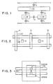
- This invention illustrated in FIGS. 2 and 3, is a technique to reduce far-end noise that requires no package design changes, except for the inclusion of floating lines at otherwise empty positions. Such floating lines could also be used to decrease impedance in such carriers where process conditions have led to greater than desirable impedance.
- the invention is based on the concept that far-end noise would be negligible in a package devoid of crossing lines and adjacent vias, because capacitive and inductive coupling are nearly equal. Other lines and vias, however, shield adjacent lines and reduce coupling.
- Inductive coupling between adjacent lines decreases only marginally, since other lines and vias constitute perpendicular elements that shield only through eddy current. Capacitive coupling, however, decreases substantially because such other lines and vias effectively block electric field.
- near-end noise benefits from reductions in either type of coupling, far-end noise increases considerably when other lines and vias are introduced.
- the capacitive coupling is increased just enough to make it equal to the inductive coupling, the far-end noise is nearly eliminated. Near-end noise would increase, but still be less than that when no other lines or vias are present.
- C x is defined as the x-line's capacitance to the reference planes
- C xy is defined as the overlap capacitance between crossing lines
- C12 is defined as the coupling capacitance between two parallel lines.
- the X-line's even mode capacitance is C x + C xy C x /(C xy + C x ), obtained by applying even symmetry about the vertical plane bisecting the structure, while the odd mode capacitance is C x + C xy + 2C12, obtained by bisecting the structure with a perfectly conducting plane.
- the new coupling capacitance is simply half their difference, C12 + 1/2[C xy - C xy C x /(C xy + C x )], with the increase given by 1/2 [C xy - C xy C x /(C xy + C x )].
- Fig. 2 shows a simple embodiment of the invention.
- the vias 10 and 12 and a long Y-line 14 represent other lines and vias that cause the difference between capacitive and inductive coupling, while the added floating lines 16 and 18 represent the invention.
- Another embodiment of the invention that enhances the floating line's effect is shown in Fig. 3 where the floating line has a configuration or shape to increase the value of C xy and the nearest reference plane is opened to reduce C y .
- Another way to increase capacitive coupling would be to place short, floating vias at otherwise empty sites, with the via having an H shaped cross section to minimize eddy current and thus inductive effects.
- the present invention is a structure that includes a plane pair of wiring, such as a multi-chip carrier, with floating lines to decrease far-end noise and to reduce impedance mismatch between different package levels.
Landscapes
- Internal Circuitry In Semiconductor Integrated Circuit Devices (AREA)
- Semiconductor Integrated Circuits (AREA)
Applications Claiming Priority (2)
| Application Number | Priority Date | Filing Date | Title |
|---|---|---|---|
| US07/383,516 US5006918A (en) | 1989-07-24 | 1989-07-24 | Floating orthogonal line structure for X-Y wiring planes |
| US383516 | 1989-07-24 |
Publications (2)
| Publication Number | Publication Date |
|---|---|
| EP0410164A2 true EP0410164A2 (de) | 1991-01-30 |
| EP0410164A3 EP0410164A3 (en) | 1991-06-05 |
Family
ID=23513510
Family Applications (1)
| Application Number | Title | Priority Date | Filing Date |
|---|---|---|---|
| EP19900112663 Withdrawn EP0410164A3 (en) | 1989-07-24 | 1990-07-03 | Floating orthogonal line structure for x-y wiring planes |
Country Status (3)
| Country | Link |
|---|---|
| US (1) | US5006918A (de) |
| EP (1) | EP0410164A3 (de) |
| JP (1) | JPH0652761B2 (de) |
Cited By (1)
| Publication number | Priority date | Publication date | Assignee | Title |
|---|---|---|---|---|
| US6043724A (en) * | 1997-12-04 | 2000-03-28 | International Business Machines Corporation | Two-stage power noise filter with on and off chip capacitors |
Families Citing this family (2)
| Publication number | Priority date | Publication date | Assignee | Title |
|---|---|---|---|---|
| JPH0770837B2 (ja) * | 1992-05-20 | 1995-07-31 | インターナショナル・ビジネス・マシーンズ・コーポレイション | 多層配線を有する電子パッケージ基板及び方法 |
| US5670815A (en) * | 1994-07-05 | 1997-09-23 | Motorola, Inc. | Layout for noise reduction on a reference voltage |
Family Cites Families (10)
| Publication number | Priority date | Publication date | Assignee | Title |
|---|---|---|---|---|
| US3904886A (en) * | 1974-02-01 | 1975-09-09 | Ibm | Voltage distribution systems for integrated circuits |
| US4212026A (en) * | 1977-06-24 | 1980-07-08 | International Business Machines Corporation | Merged array PLA device, circuit, fabrication method and testing technique |
| US4589008A (en) * | 1980-01-28 | 1986-05-13 | Rca Corporation | Apparatus for electrically joining the ends of substantially parallel semiconductor lines |
| US4423432A (en) * | 1980-01-28 | 1983-12-27 | Rca Corporation | Apparatus for decoding multiple input lines |
| JPS6030152A (ja) * | 1983-07-28 | 1985-02-15 | Toshiba Corp | 集積回路 |
| US4583111A (en) * | 1983-09-09 | 1986-04-15 | Fairchild Semiconductor Corporation | Integrated circuit chip wiring arrangement providing reduced circuit inductance and controlled voltage gradients |
| US4770921A (en) * | 1986-09-11 | 1988-09-13 | Insulating Materials Incorporated | Self-shielding multi-layer circuit boards |
| US4825280A (en) * | 1986-10-01 | 1989-04-25 | Texas Instruments Incorporated | Electrostatic discharge protection for semiconductor devices |
| DE3902693C2 (de) * | 1988-01-30 | 1995-11-30 | Toshiba Kawasaki Kk | Mehrebenenverdrahtung für eine integrierte Halbleiterschaltungsanordnung und Verfahren zur Herstellung von Mehrebenenverdrahtungen für integrierte Halbleiterschaltungsanordnungen |
| US4845538A (en) * | 1988-02-05 | 1989-07-04 | Emanuel Hazani | E2 prom cell including isolated control diffusion |
-
1989
- 1989-07-24 US US07/383,516 patent/US5006918A/en not_active Expired - Fee Related
-
1990
- 1990-07-03 EP EP19900112663 patent/EP0410164A3/en not_active Withdrawn
- 1990-07-20 JP JP2190902A patent/JPH0652761B2/ja not_active Expired - Lifetime
Cited By (1)
| Publication number | Priority date | Publication date | Assignee | Title |
|---|---|---|---|---|
| US6043724A (en) * | 1997-12-04 | 2000-03-28 | International Business Machines Corporation | Two-stage power noise filter with on and off chip capacitors |
Also Published As
| Publication number | Publication date |
|---|---|
| EP0410164A3 (en) | 1991-06-05 |
| JPH0652761B2 (ja) | 1994-07-06 |
| JPH0370161A (ja) | 1991-03-26 |
| US5006918A (en) | 1991-04-09 |
Similar Documents
| Publication | Publication Date | Title |
|---|---|---|
| US6218631B1 (en) | Structure for reducing cross-talk in VLSI circuits and method of making same using filled channels to minimize cross-talk | |
| JP3530920B2 (ja) | 多層パッケージ、パッケージング方法及び多層パッケージ化半導体装置 | |
| EP0766503B1 (de) | Mehrschichtige gedruckte Schaltungsplatte und ihre Verwendung als Kontaktgitterpackung | |
| US20050225955A1 (en) | Multi-layer printed circuit boards | |
| US5994766A (en) | Flip chip circuit arrangement with redistribution layer that minimizes crosstalk | |
| US5446243A (en) | Post processing shielding | |
| US7904849B2 (en) | Ceramic package in which far end noise is reduced using capacitive cancellation by offset wiring | |
| US6884706B2 (en) | High permeability thin films and patterned thin films to reduce noise in high speed interconnections | |
| US20030174529A1 (en) | High permeability layered films to reduce noise in high speed interconnects | |
| US20050263793A1 (en) | Wire bonding method and apparatus for integrated circuit | |
| EP1421620B1 (de) | Integrierte Schaltung mit Signalleitungen und gitterartige Schicht | |
| US6215076B1 (en) | Printed circuit board with noise suppression | |
| JP2988421B2 (ja) | Emi抑制多層プリント基板 | |
| US7209368B2 (en) | Circuitized substrate with signal wire shielding, electrical assembly utilizing same and method of making | |
| US5006918A (en) | Floating orthogonal line structure for X-Y wiring planes | |
| US20030127728A1 (en) | Concurrent electrical signal wiring optimization for an electronic package | |
| US7375411B2 (en) | Method and structure for forming relatively dense conductive layers | |
| US5126822A (en) | Supply pin rearrangement for an I.C. | |
| EP0382948A1 (de) | Versorgungssteckerstift-Anordnung für eine integrierte Schaltung | |
| US6559733B2 (en) | Reducing effects of electrical impedance | |
| JPH03158002A (ja) | 半導体装置 | |
| Schaper et al. | Design of the Interconnected Mesh Power System (IMPS) MCM Topology | |
| EP0558984A2 (de) | Keramische Hybrid-Modulstruktur vom Dünnschicht-Typ | |
| Russ et al. | Coupled noise and its effects on modern packaging technology | |
| Kinniment et al. | Influence of circuit layout and packaging on fast computer performance |
Legal Events
| Date | Code | Title | Description |
|---|---|---|---|
| PUAI | Public reference made under article 153(3) epc to a published international application that has entered the european phase |
Free format text: ORIGINAL CODE: 0009012 |
|
| AK | Designated contracting states |
Kind code of ref document: A2 Designated state(s): DE FR GB |
|
| 17P | Request for examination filed |
Effective date: 19901213 |
|
| PUAL | Search report despatched |
Free format text: ORIGINAL CODE: 0009013 |
|
| AK | Designated contracting states |
Kind code of ref document: A3 Designated state(s): DE FR GB |
|
| 17Q | First examination report despatched |
Effective date: 19940321 |
|
| STAA | Information on the status of an ep patent application or granted ep patent |
Free format text: STATUS: THE APPLICATION IS DEEMED TO BE WITHDRAWN |
|
| 18D | Application deemed to be withdrawn |
Effective date: 19970201 |