EP0410023A1 - Procédé et appareil pour la préparation d'un ruban à fibres optiques - Google Patents
Procédé et appareil pour la préparation d'un ruban à fibres optiques Download PDFInfo
- Publication number
- EP0410023A1 EP0410023A1 EP89113580A EP89113580A EP0410023A1 EP 0410023 A1 EP0410023 A1 EP 0410023A1 EP 89113580 A EP89113580 A EP 89113580A EP 89113580 A EP89113580 A EP 89113580A EP 0410023 A1 EP0410023 A1 EP 0410023A1
- Authority
- EP
- European Patent Office
- Prior art keywords
- optical fibers
- guide
- sheet
- fusion
- shaped photoconductor
- Prior art date
- Legal status (The legal status is an assumption and is not a legal conclusion. Google has not performed a legal analysis and makes no representation as to the accuracy of the status listed.)
- Granted
Links
- 239000013307 optical fiber Substances 0.000 title claims abstract description 67
- 238000000034 method Methods 0.000 title claims description 12
- 238000002360 preparation method Methods 0.000 title claims description 9
- 238000009987 spinning Methods 0.000 claims abstract description 23
- 239000000835 fiber Substances 0.000 claims abstract description 17
- 238000002074 melt spinning Methods 0.000 claims abstract description 8
- 230000004927 fusion Effects 0.000 claims abstract 2
- 230000002093 peripheral effect Effects 0.000 claims description 4
- 238000010438 heat treatment Methods 0.000 claims description 3
- 229920000642 polymer Polymers 0.000 description 7
- 230000005540 biological transmission Effects 0.000 description 5
- 239000000306 component Substances 0.000 description 4
- 239000004020 conductor Substances 0.000 description 4
- YCKRFDGAMUMZLT-UHFFFAOYSA-N Fluorine atom Chemical compound [F] YCKRFDGAMUMZLT-UHFFFAOYSA-N 0.000 description 3
- 238000004132 cross linking Methods 0.000 description 3
- 229910052731 fluorine Inorganic materials 0.000 description 3
- 239000011737 fluorine Substances 0.000 description 3
- 229920003229 poly(methyl methacrylate) Polymers 0.000 description 3
- 229920000058 polyacrylate Polymers 0.000 description 3
- 239000004926 polymethyl methacrylate Substances 0.000 description 3
- CERQOIWHTDAKMF-UHFFFAOYSA-M Methacrylate Chemical compound CC(=C)C([O-])=O CERQOIWHTDAKMF-UHFFFAOYSA-M 0.000 description 2
- 239000008358 core component Substances 0.000 description 2
- 238000004519 manufacturing process Methods 0.000 description 2
- 230000003287 optical effect Effects 0.000 description 2
- 238000001125 extrusion Methods 0.000 description 1
- 230000009477 glass transition Effects 0.000 description 1
- 239000000463 material Substances 0.000 description 1
- 238000002844 melting Methods 0.000 description 1
- 230000008018 melting Effects 0.000 description 1
- 239000004033 plastic Substances 0.000 description 1
- 229920003023 plastic Polymers 0.000 description 1
- 239000004417 polycarbonate Substances 0.000 description 1
- 229920000515 polycarbonate Polymers 0.000 description 1
- 229920005573 silicon-containing polymer Polymers 0.000 description 1
- 229920005992 thermoplastic resin Polymers 0.000 description 1
Images


Classifications
-
- G—PHYSICS
- G02—OPTICS
- G02B—OPTICAL ELEMENTS, SYSTEMS OR APPARATUS
- G02B6/00—Light guides; Structural details of arrangements comprising light guides and other optical elements, e.g. couplings
- G02B6/04—Light guides; Structural details of arrangements comprising light guides and other optical elements, e.g. couplings formed by bundles of fibres
- G02B6/06—Light guides; Structural details of arrangements comprising light guides and other optical elements, e.g. couplings formed by bundles of fibres the relative position of the fibres being the same at both ends, e.g. for transporting images
- G02B6/08—Light guides; Structural details of arrangements comprising light guides and other optical elements, e.g. couplings formed by bundles of fibres the relative position of the fibres being the same at both ends, e.g. for transporting images with fibre bundle in form of plate
Definitions
- the present invention relates to a process and apparatus for the preparation of a sheet-shaped photoconductor that can be used for various image guides or as a photoconductive material.
- a sheet-shaped photoconductor comprising optical fibers is used as an element of an image guide or a photoconductor for various display devices.
- As the process for continuously preparing this sheet-shaped photoconductor there is known a process in which many optical fibers are arranged in the form of a sheet by a comb-like guide and piano wires and then are bonded and fixed, as disclosed in Japanese Examined Patent Publication No. 52-38419. If, however, the optical fibers are forcibly passed through the guide, the outer surfaces of the optical fibers are damaged and the optical properties are lowered. Moreover, since the bonding step is indispensable, the operation is complicated and the manufacturing cost is increased.
- Japanese Unexamined Patent Publication No. 50-8540 proposes a process in which many optical fibers are melt-spun, and the spun optical fibers are fusion-bonded in parallel to one another while the as-spun fibers are maintained at a temperature higher than the glass transition temperature, whereby a tape-shaped photoconductor is prepared.
- the post bonding treatment becomes unnecessary, but since the fibers are arranged in the form of a sheet by a rod-shaped width-regulating guide arranged downstream of a spinning nozzle, the optical fibers spun cylindrically and concentrically must be immediately linearly arranged in parallel to one another.
- this width-regulating guide has a rod-like shape, the difference of the yarn tension of optical fibers spun from the central portion of the spinning nozzle from that of optical fibers spun from the peripheral portion of the spinning nozzle is large, and therefore, it is difficult to stably guide the optical fibers. Accordingly, yarn unevenness occurs or an overlapping of the optical fibers occurs locally in the sheet-like arrangement of the optical fibers, with the result that it is difficult to obtain a sheet having a uniform width, and an optical fiber sheet not having uniform optical transmission characteristics is often formed.
- a primary object of the present invention is to provide a process and apparatus in which a sheet-shaped photoconductor having excellent light transmission characteristics, a uniform width, and no overlapped portions, can be prepared at a high efficiency.
- a process for the preparation of a sheet-shaped photoconductor which comprises melt-spinning a spinning dope into a plurality of optical fibers, and bonding them to one another along the entire length thereof before the optical fibers are cooled, to form a sheet-shaped photoconductor in which the optical fibers are arranged in parallel, wherein the optical fibers are melt-spun from a spinning nozzle having a plurality of orifices annularly arranged; the as-spun optical fibers are arranged linearly in parallel to but not in contact with one another and then the optical fibers are brought into contact with and fusion-bonded to one another; and the thus-formed sheet-shaped photoconductor is taken up.
- an apparatus for the preparation of a sheet-shaped photoconductor which comprises a nozzle having a plurality of annularly arranged orifices for melt-extruding a spinning dope for optical fibers; a grooved guide arranged so that the axis thereof extends in the vertical direction to the spinning axis of the melt-spinning nozzle, and having a plurality of grooves extending in the peripheral direction of the grooved guide; a fusion-bonding guide having a concave curved face in the central portion, which is arranged so that the axis thereof is substantially in parallel to the axis of the grooved guide; and a take-up roller for taking up a formed sheet-shaped photoconductor.
- Figure 1 is a schematic front view of the apparatus of the present invention.
- optical fibers F1 are melt-spun from a spinning nozzle having many orifices 11 annularly arranged therein (shown in the bottom view of Fig. 2).
- a grooved guide 2 is arranged so that the axis thereof extends substantially in the vertical direction to the axis of the spinning nozzle 1 and has a number of grooves formed therein equal to or larger than the number of the orifices.
- the grooves extend in the peripheral direction of the grooved guide.
- each groove the grooved guide 2 is not particularly critical, as long as contact between the optical fibers F1 is prevented.
- V-shaped grooves and U-shaped grooves can be used.
- an auxiliary guide 3 is arranged so that the axis thereof is in parallel to the axis of the grooved guide 2 with a certain distance therebetween, as shown in Figs.
- the auxiliary guide 3 is located in a position such that the optical fibers F2 traveling from the grooved guide 2 is slightly deviated whereby a certain tension is imposed on the optical fibers F2.
- a fusion-bonding guide 4 has a concave curved face formed in the vicinity of the center thereof for arranging the optical fibers F3 in parallel to one another and fusion-bonding them in this parallel state.
- the fusion-bonded optical fibers F4 are taken up in the form of a sheet-shaped photoconductor by a first nip roller 5 (shown in Fig. 1).
- the optical fibers F1 flow smoothly and substantially linearly in the grooves, no strain is imposed on the optical fibers F1. Then a tension is applied to the optical fibers F2 by the auxiliary guide 3 located downstream, to stabilize traveling of the optical fibers. At this point, the optical fibers F2 are not fusion-bonded to one another and arrive independently at the fusion-bonding guide 4. Since the fusion-bonding guide 4 has a concave curved face in the central portion, the optical fibers F3 are gathered and fusion-bonded to one another as shown in Fig. 3.
- the structures as shown in Figs 5A through 5C can be adopted for the fusion-bonding guide 4. More specifically, a structure having a curvature R1 as shown in Fig.
- a structure having a curvature R2 on both of the left and right sides as shown in Fig. 5B, and a structure having a V-shaped groove and a curvature R3 at the center of the groove as shown in Fig. 5C can be adopted.
- the thus-combined optical fibers F4 are substantially linearly arranged and fusion-bonded to one another and are taken up in this state by the nip roller 5 acting as the take-up roller.
- the sheet-shaped photoconductor of the optical fibers can be prepared in the above-mentioned manner.
- Figure 6 shows an embodiment of the fusion-bonding guide which is the same as the guide 4 shown in Figs. 1 and 3 except that the fusion-bonding guide in Fig. 6 is designed so that a plurality of sheet-shaped photoconductors can be prepared by using one spinning nozzle. More specifically, the fusion-bonding guide having a structure as shown in Fig. 6 is arranged instead of the fusion-bonding guide 4 shown in Fig. 1 in the apparatus of the present invention.
- the as-spun optical fibers are divided into a plurality of groups and are linearly distributed and arranged in a plurality of concave curved faces by this fusion-bonding guide, and each group of fibers are fusion-bonded to one another in this state to obtain a plurality of sheet-shaped photoconductors having different widths or the same widths.
- Figures 7A and 7B show the section of a part of the sheet-shaped photoconductor prepared in the present invention; wherein Fig. 7A shows an example composed of optical fibers having a two-layer structure comprising a core Fa and a sheath Fb, and Fig. 7B shows an example composed of optical fibers having a three-layer structure comprising a core Fa, a sheath Fb, and a protecting layer Fc.
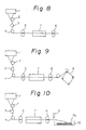
- Figure 8 illustrates another embodiment of the process for preparing a sheet-shaped photoconductor by using the apparatus of the present invention.
- a second take-up roller (nip roller) 6 is arranged downstream of the first take-up roller (nip roller) 5, and a heating device 7 is disposed between the two nip rollers 5 and 6.
- the sheet-shaped photoconductor can be subjected to hot drawing between the first and second nip rollers 5 and 6, whereby a high tenacity can be given to the optical fibers.
- Figure 9 illustrates still another embodiment in which a reeling winder 8 is arranged in the rear of the second nip roller 6 shown in Fig. 8.
- the sheet-shaped photoconductor is wound on the reeling winder 8 and is overlapped in multiple layers, and the laminate is fixed and cut at the respective corners to prepare optical fiber bands having a length corresponding to one side of the reeling winder 8.
- Figure 10 illustrates an embodiment in which a sheet-shaped photoconductor F5 having a certain length is obtained.
- a cutter 9 is arranged behind the second nip roller 6 to cut the sheet-shaped photoconductor to predetermined lengths, and the cut photoconductors are stored in a container case 10.
- optical fiber used in the present invention is not particularly critical, as long as melt spinning is possible, but plastic type optical fibers having a core composed of a thermoplastic resin such as an acrylic polymer, a polycarbonate or a polyallylate or a crosslinking-curing polymer such as a crosslinking silicone polymer, a crosslinking acrylate polymer, or an ion-crosslinking polymer and a sheath composed of a polymer having a refractive index smaller than that of the core polymer, such as a fluorine-containing polymer or an acrylic polymer, are preferably used.
- An appropirate protecting layer can be selected according to the intended use.
- a sheet-shaped photoconductor was prepared by using the preparation apparatus shown in Fig. 1.
- a conjugate spinning nozzle 1 having 100 orifices 11 arranged annularly was used, and polymethyl methacrylate was supplied as the core component at a rate of 1.07 g/min per orifice and a fluorine-containing methacrylate polymer was supplied as the sheath component at a rate of 0.08 g/min per orifice.
- Conjugate melt spinning was carried out at a spinning temperature of 255°C, and then the spun fibers were passed through a grooved guide 2, an auxiliary guide 3, and a fusion-bonding guide 4, and a formed sheet-shaped photoconductor was taken up at a take-up speed of 120 m/min by a nip roller 5.
- the distance l1 between the spinning nozzle 1 and the grooved guide 2 was adjusted to 300 mm
- the distance l2 between the grooved guide 2 and the auxiliary guide 3 was adjusted to 50 mm
- the distance l3 between the auxiliary guide 3 and the fusion-bonding guide 4 was adjusted to 50 mm.
- the grooved guide 2, auxiliary guide 3, and fusion-bonding guide 4 were forcibly cooled so that the surface temperature of these guides were maintained at the same level.
- optical fibers, each having a diameter of 100 ⁇ m were uniformly arranged linearly in parallel to one another, and the width of the sheet-shaped photoconductor was 10 mm.
- the single fiber diameter in the 100 optical fibers was within 100 ⁇ m ⁇ 1 ⁇ m, and the light transmission performance was as high as 285 dB/km ⁇ 30 dB/km.
- a sheet-shaped photoconductor was prepared by arranging a fusion-bonding guide having a structure as shown in Fig. 6 in the same apparatus as used in Example 1.
- Polymethyl methacrylate was supplied as the core component at a rate of 2.45 g/min per orifice
- a fluorine-containing methacrylate polymer was supplied as the sheath component at a rate of 0.15 g/min per orifice
- polymethyl methacrylate was supplied as the protecting layer component at a rate of 0.13 g/min per orifice.
- Conjugate spinning was carried out at a spinning temperature of 250°C, the spun fibers were divided into 4 groups, each consisting of 25 fibers, by the fusion-bonding guide, the optical fibers were taken up at a speed of 50 m/min, and sheet-shaped photoconductors were prepared by using a heating device 7 as shown in Fig. 8 (the inner temperature was adjusted to 200°C). Note, the take-up speed of the second nip roller 6 was adjusted to 51 m/min to draw the photoconductors at a draw ratio of 1.05.
- the single fiber diameter was 250 ⁇ m and the sheet width was 6.25 mm, and the single fiber diameter in the 100 fibers was within 250 ⁇ m ⁇ 2 ⁇ m and the light transmission performance was within 230 dB/km ⁇ 20 dB/km. None of the sheet-shaped photoconductors had a meandering strain but was very pliable.
- a sheet-shaped photoconductor having good light transmission characteristics, and which is uniform without local overlapping or meandering strain, can be prepared at a high efficiency.
Landscapes
- Physics & Mathematics (AREA)
- General Physics & Mathematics (AREA)
- Optics & Photonics (AREA)
- Optical Fibers, Optical Fiber Cores, And Optical Fiber Bundles (AREA)
- Spinning Methods And Devices For Manufacturing Artificial Fibers (AREA)
Priority Applications (3)
| Application Number | Priority Date | Filing Date | Title |
|---|---|---|---|
| DE68918854T DE68918854T2 (de) | 1989-07-24 | 1989-07-24 | Verfahren und Vorrichtung zur Herstellung eines Lichtleiterbandes. |
| EP89113580A EP0410023B1 (fr) | 1989-07-24 | 1989-07-24 | Procédé et appareil pour la préparation d'un ruban à fibres optiques |
| US07/385,384 US4980012A (en) | 1989-07-24 | 1989-07-25 | Apparatus for preparation of a sheet-shaped photoconductor |
Applications Claiming Priority (1)
| Application Number | Priority Date | Filing Date | Title |
|---|---|---|---|
| EP89113580A EP0410023B1 (fr) | 1989-07-24 | 1989-07-24 | Procédé et appareil pour la préparation d'un ruban à fibres optiques |
Publications (2)
| Publication Number | Publication Date |
|---|---|
| EP0410023A1 true EP0410023A1 (fr) | 1991-01-30 |
| EP0410023B1 EP0410023B1 (fr) | 1994-10-12 |
Family
ID=8201675
Family Applications (1)
| Application Number | Title | Priority Date | Filing Date |
|---|---|---|---|
| EP89113580A Expired - Lifetime EP0410023B1 (fr) | 1989-07-24 | 1989-07-24 | Procédé et appareil pour la préparation d'un ruban à fibres optiques |
Country Status (3)
| Country | Link |
|---|---|
| US (1) | US4980012A (fr) |
| EP (1) | EP0410023B1 (fr) |
| DE (1) | DE68918854T2 (fr) |
Families Citing this family (12)
| Publication number | Priority date | Publication date | Assignee | Title |
|---|---|---|---|---|
| EP0371432B1 (fr) * | 1988-11-28 | 1995-07-05 | Mitsubishi Rayon Co., Ltd. | Méthode de fabrication d'un écran du type à transmission |
| US5115260A (en) * | 1990-09-04 | 1992-05-19 | International Business Machines Corporation | Compact strain relief device for fiber optic cables |
| US5160569A (en) * | 1991-08-08 | 1992-11-03 | Siecor Corporation | Tool for preparing optical ribbons |
| US5348586A (en) * | 1993-10-29 | 1994-09-20 | Siecor Corporation | Ribbon prewet system |
| US6115523A (en) * | 1996-10-04 | 2000-09-05 | University Of Florida | Plastic optical fiber airway imaging system |
| US20040220451A1 (en) * | 1996-10-04 | 2004-11-04 | Dietrich Gravenstein | Imaging scope |
| US6322498B1 (en) | 1996-10-04 | 2001-11-27 | University Of Florida | Imaging scope |
| US20050182297A1 (en) * | 1996-10-04 | 2005-08-18 | Dietrich Gravenstein | Imaging scope |
| MXPA03002112A (es) | 2000-09-15 | 2004-09-10 | First Quality Fibers Llc | Aparato para fabricar fibra optica hecha de polimero semicristalino. |
| EP2370244A2 (fr) * | 2008-12-04 | 2011-10-05 | Eidgenössische Technische Hochschule Zürich | Articles polymères, procédés et matrices pour produire lesdits articles |
| JP5864119B2 (ja) * | 2011-03-30 | 2016-02-17 | 昭和電線ケーブルシステム株式会社 | 光ファイバテープ心線の製造方法 |
| CN109130185B (zh) * | 2018-10-25 | 2021-01-05 | 哈尔滨工程大学 | 一种滚压式连续纤维光固化3d打印装置 |
Citations (4)
| Publication number | Priority date | Publication date | Assignee | Title |
|---|---|---|---|---|
| JPS508540A (fr) * | 1973-05-21 | 1975-01-29 | ||
| JPS5238419B2 (fr) * | 1973-08-29 | 1977-09-29 | ||
| EP0131058A1 (fr) * | 1983-06-22 | 1985-01-16 | Mitsubishi Rayon Co., Ltd. | Assemblage de fibres optiques et procédé pour sa préparation |
| EP0165632A2 (fr) * | 1984-05-23 | 1985-12-27 | Koninklijke Philips Electronics N.V. | Câble optique plat, procédé pour fabriquer celui-ci, et câble optique composé de plusieurs câbles optiques plats |
Family Cites Families (6)
| Publication number | Priority date | Publication date | Assignee | Title |
|---|---|---|---|---|
| GB1284114A (en) * | 1968-08-24 | 1972-08-02 | Toyo Boseki | Tape-shaped assembly of elastic filaments and its production |
| US4195161A (en) * | 1973-09-26 | 1980-03-25 | Celanese Corporation | Polyester fiber |
| DE2838977C3 (de) * | 1978-09-07 | 1984-11-08 | J.H. Benecke Gmbh, 3000 Hannover | Vorrichtung zur Verhinderung des Umspringens der Filamente in einer Filament-Spinnvlies-Anlage |
| US4379771A (en) * | 1980-05-23 | 1983-04-12 | Western Electric Company, Inc. | Methods of and apparatus for terminating a lightguide fiber ribbon |
| JPS6125115A (ja) * | 1984-07-13 | 1986-02-04 | Sumitomo Electric Ind Ltd | 光フアイバ2心コ−ドの製造方法 |
| CA1248313A (fr) * | 1985-05-13 | 1989-01-10 | Yoshitaka Ohsawa | Production d'une fibre optique elastomere |
-
1989
- 1989-07-24 DE DE68918854T patent/DE68918854T2/de not_active Expired - Fee Related
- 1989-07-24 EP EP89113580A patent/EP0410023B1/fr not_active Expired - Lifetime
- 1989-07-25 US US07/385,384 patent/US4980012A/en not_active Expired - Lifetime
Patent Citations (4)
| Publication number | Priority date | Publication date | Assignee | Title |
|---|---|---|---|---|
| JPS508540A (fr) * | 1973-05-21 | 1975-01-29 | ||
| JPS5238419B2 (fr) * | 1973-08-29 | 1977-09-29 | ||
| EP0131058A1 (fr) * | 1983-06-22 | 1985-01-16 | Mitsubishi Rayon Co., Ltd. | Assemblage de fibres optiques et procédé pour sa préparation |
| EP0165632A2 (fr) * | 1984-05-23 | 1985-12-27 | Koninklijke Philips Electronics N.V. | Câble optique plat, procédé pour fabriquer celui-ci, et câble optique composé de plusieurs câbles optiques plats |
Non-Patent Citations (1)
| Title |
|---|
| THE TRANSACTIONS OF THE IECE OF JAPAN, vol. E-61, no. 3, March 1978, pages 175-177; H. SUZUKI et al.: "Flat type Cable with Silicone Clad Optical Fibres" * |
Also Published As
| Publication number | Publication date |
|---|---|
| US4980012A (en) | 1990-12-25 |
| EP0410023B1 (fr) | 1994-10-12 |
| DE68918854D1 (de) | 1994-11-17 |
| DE68918854T2 (de) | 1995-05-11 |
Similar Documents
| Publication | Publication Date | Title |
|---|---|---|
| EP0410023B1 (fr) | Procédé et appareil pour la préparation d'un ruban à fibres optiques | |
| US5442722A (en) | Optical fiber ribbon with zip cord | |
| US4547040A (en) | Optical fiber assembly and process for preparing same | |
| CA1121194A (fr) | Cable de fibres optiques, et methode d'assemblage connexe | |
| CN107209337B (zh) | 松套管、松套管型光纤电缆、松套管的光纤带的单芯分离方法、松套管的制造方法及多根光纤的集线方法 | |
| US3969016A (en) | Low dispersion optical fiber wave guiding structures with periodically deformed waveguide axis | |
| US5189721A (en) | Optical fiber ribbon cable | |
| WO1993016408A1 (fr) | Cable-ruban a fibres optiques | |
| US20030031434A1 (en) | Method for making separable multiple core optical fibers, the resulting fiber structures, and uses thereof | |
| CN102016673A (zh) | 多纤维光缆 | |
| US20040240806A1 (en) | Fiber optic cable having a binder | |
| KR0160492B1 (ko) | 투과형 스크린 및 그 제조방법 | |
| EP0131058A1 (fr) | Assemblage de fibres optiques et procédé pour sa préparation | |
| US5420955A (en) | Optical cables having U-shaped carriers exhibiting enhanced crush performance | |
| KR930005097B1 (ko) | 멀티필라멘트 광섬유의 제조방법 | |
| KR920006590B1 (ko) | 시트-형 광전도체 형성 방법 및 장치 | |
| JPH01130106A (ja) | 光減衰器とその製造方法 | |
| JPH01224704A (ja) | シート状導光体の製造方法及びその製造装置 | |
| GB2079970A (en) | Improvements in or relating to optical cable elements | |
| JP2777833B2 (ja) | 投写スクリーンの製造方法及び両面レンチキュラーレンズ | |
| JP2849767B2 (ja) | 投写スクリーンの製造方法 | |
| JPH03296007A (ja) | プラスチック光ファイバコードの製造方法 | |
| EP0510513B1 (fr) | Coupleur à fibre optique et méthode de sa fabrication | |
| US20230408786A1 (en) | Optical-fiber ribbon, die, and method of manufacturing optical-fiber ribbon | |
| JPS60117202A (ja) | シ−ト状導光体の製造方法およびその製造装置 |
Legal Events
| Date | Code | Title | Description |
|---|---|---|---|
| PUAI | Public reference made under article 153(3) epc to a published international application that has entered the european phase |
Free format text: ORIGINAL CODE: 0009012 |
|
| 17P | Request for examination filed |
Effective date: 19890724 |
|
| AK | Designated contracting states |
Kind code of ref document: A1 Designated state(s): DE FR GB IT |
|
| 17Q | First examination report despatched |
Effective date: 19930302 |
|
| GRAA | (expected) grant |
Free format text: ORIGINAL CODE: 0009210 |
|
| AK | Designated contracting states |
Kind code of ref document: B1 Designated state(s): DE FR GB IT |
|
| REF | Corresponds to: |
Ref document number: 68918854 Country of ref document: DE Date of ref document: 19941117 |
|
| ET | Fr: translation filed | ||
| ITF | It: translation for a ep patent filed | ||
| PG25 | Lapsed in a contracting state [announced via postgrant information from national office to epo] |
Ref country code: GB Effective date: 19950724 |
|
| PLBE | No opposition filed within time limit |
Free format text: ORIGINAL CODE: 0009261 |
|
| STAA | Information on the status of an ep patent application or granted ep patent |
Free format text: STATUS: NO OPPOSITION FILED WITHIN TIME LIMIT |
|
| 26N | No opposition filed | ||
| GBPC | Gb: european patent ceased through non-payment of renewal fee |
Effective date: 19950724 |
|
| PG25 | Lapsed in a contracting state [announced via postgrant information from national office to epo] |
Ref country code: DE Effective date: 19960402 |
|
| PG25 | Lapsed in a contracting state [announced via postgrant information from national office to epo] |
Ref country code: FR Effective date: 19960430 |
|
| REG | Reference to a national code |
Ref country code: FR Ref legal event code: ST |
|
| REG | Reference to a national code |
Ref country code: FR Ref legal event code: ST |
|
| REG | Reference to a national code |
Ref country code: FR Ref legal event code: ST |
|
| PG25 | Lapsed in a contracting state [announced via postgrant information from national office to epo] |
Ref country code: IT Free format text: LAPSE BECAUSE OF NON-PAYMENT OF DUE FEES Effective date: 20050724 |