EP0408464B1 - Unité pour des opérations logiques sur zones binaires et microprocesseur en comprenant ladite unité - Google Patents
Unité pour des opérations logiques sur zones binaires et microprocesseur en comprenant ladite unité Download PDFInfo
- Publication number
- EP0408464B1 EP0408464B1 EP90402037A EP90402037A EP0408464B1 EP 0408464 B1 EP0408464 B1 EP 0408464B1 EP 90402037 A EP90402037 A EP 90402037A EP 90402037 A EP90402037 A EP 90402037A EP 0408464 B1 EP0408464 B1 EP 0408464B1
- Authority
- EP
- European Patent Office
- Prior art keywords
- logic operation
- bit
- mask pattern
- logic
- pattern generation
- Prior art date
- Legal status (The legal status is an assumption and is not a legal conclusion. Google has not performed a legal analysis and makes no representation as to the accuracy of the status listed.)
- Expired - Lifetime
Links
Images


Classifications
-
- G—PHYSICS
- G06—COMPUTING OR CALCULATING; COUNTING
- G06F—ELECTRIC DIGITAL DATA PROCESSING
- G06F7/00—Methods or arrangements for processing data by operating upon the order or content of the data handled
- G06F7/76—Arrangements for rearranging, permuting or selecting data according to predetermined rules, independently of the content of the data
- G06F7/764—Masking
-
- G—PHYSICS
- G06—COMPUTING OR CALCULATING; COUNTING
- G06F—ELECTRIC DIGITAL DATA PROCESSING
- G06F9/00—Arrangements for program control, e.g. control units
- G06F9/06—Arrangements for program control, e.g. control units using stored programs, i.e. using an internal store of processing equipment to receive or retain programs
- G06F9/30—Arrangements for executing machine instructions, e.g. instruction decode
- G06F9/30003—Arrangements for executing specific machine instructions
- G06F9/30007—Arrangements for executing specific machine instructions to perform operations on data operands
- G06F9/30018—Bit or string instructions
-
- G—PHYSICS
- G06—COMPUTING OR CALCULATING; COUNTING
- G06F—ELECTRIC DIGITAL DATA PROCESSING
- G06F9/00—Arrangements for program control, e.g. control units
- G06F9/06—Arrangements for program control, e.g. control units using stored programs, i.e. using an internal store of processing equipment to receive or retain programs
- G06F9/30—Arrangements for executing machine instructions, e.g. instruction decode
- G06F9/30003—Arrangements for executing specific machine instructions
- G06F9/30007—Arrangements for executing specific machine instructions to perform operations on data operands
- G06F9/30029—Logical and Boolean instructions, e.g. XOR, NOT
-
- G—PHYSICS
- G06—COMPUTING OR CALCULATING; COUNTING
- G06F—ELECTRIC DIGITAL DATA PROCESSING
- G06F9/00—Arrangements for program control, e.g. control units
- G06F9/06—Arrangements for program control, e.g. control units using stored programs, i.e. using an internal store of processing equipment to receive or retain programs
- G06F9/30—Arrangements for executing machine instructions, e.g. instruction decode
- G06F9/30003—Arrangements for executing specific machine instructions
- G06F9/30007—Arrangements for executing specific machine instructions to perform operations on data operands
- G06F9/30036—Instructions to perform operations on packed data, e.g. vector, tile or matrix operations
- G06F9/30038—Instructions to perform operations on packed data, e.g. vector, tile or matrix operations using a mask
Definitions
- This invention relates to a logic operation unit (LU) adapted for use in a computer system, more particularly, a bit field logic operation unit which performs a logic operation accompanied by a masking operation of a part of an operand.
- LU logic operation unit
- a logic operation such as AND, OR, EOR and the like accompanied by a masking operation is sometimes required.
- a bit or bits to be masked are specified by mask information,
- a bit or bits of an operand in the specified bit position are not altered by the logic operation, and only a remaining bit or bits are altered by the logic operation.
- This kind of operation can be performed by carrying out the following three processes:
- the logic operation accompanied by the mark operation is realized by controlling an ALU (Arithmetic Logic Unit) provided in the computer system according to a microprogram which is constituted from three microinstructions which correspond to these three processes 1) to 3), respectively.
- ALU Arimetic Logic Unit
- An object of the present invention is to provide a bit field logic operation unit which can perform a logic operation accompanied by a mask operation, within one machine cycle.
- Another object of the present invention is to provide the aforementioned bit field logic operation unit, wherein the unit is constituted from a small number of elements and the power consumption thereof is small.
- Still another object of the present invention is to provide a monolithic microprocessor wherein a bit manipulation instruction can be quickly executed, in particular, to provide a monolithic microprocessor wherein a variable-length bit field manipulation instruction, for example, an instruction to perform a specified logic operation on variable-length bit fields of a source data and a destination data and to store the operation result into a bit field of the destination side, can be executed within a smaller number of machine cycles.
- a bit manipulation instruction can be quickly executed
- a variable-length bit field manipulation instruction for example, an instruction to perform a specified logic operation on variable-length bit fields of a source data and a destination data and to store the operation result into a bit field of the destination side
- a bit field logic operation unit according to the precharacterising part of claims 1 and 6 is known from EP-A-0 171 190.
- the known unit comprises a logic operation means for performing a specified logic operation on source data and destination data to output a logic operation result, a mask pattern generation means for simultaneously calculating a bit mask pattern from mask information in parallel with the operation of the logic operation means, and a bit map operation means for selecting either the logic operation result or the destination data in each bit position according to the bit mask pattern to output a masked logic operation result.
- the logic operation means and the mask pattern generation means are constituted by dynamic circuit constructions where the processes are performed in a precharge period to charge circuit elements according to input signals, and an active period to output processed data.
- precharge period of the logic operation means and the precharge period of the mask pattern generation means are carried out simultaneously.
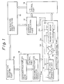
- Figure 1 shows a construction of an example of monolithic microprocessor, formed in a single semiconductor body comprising a logic operation unit according to the present invention.
- An instruction prefetching part 10 sends an instruction address to an address translation part 12 and issues an instruction prefetch request to the address translation part 12.
- the address translation part 12 translates the logical address into a physical address and transfers the translated address to an I/O control part 14.
- the I/O control part 14 prefetches an instruction and transfers it to the instruction prefetching part 10.
- the instruction prefetching part 10 transfers the prefetched instruction to an instruction decoding part 16.
- the instruction decoding part 16 decodes the instruction and transfers decoded information such as an origin address of microinstructions to an operation control part 18.
- the operation control part 18 sequentially reads out microinstructions from a microinstruction ROM 20 based on the origin address of microinstructions, stores each microinstruction into a microinstruction register 22, and controls an instruction executing part 24 according to the stored microinstruction and other decoded information to execute the instruction.
- the instruction executing part 24 comprises various types of operation units such as an ALU (Arithmetic Logic Unit) 26, a logic operation unit 28, and a register group 30.
- the operation units and the register groups 30 can exchange data with each other through buses 32, 34, and 36.
- a bit manipulation instruction, a variable-length bit field manipulation instruction, or the like is transferred from the instruction decoding part 16 to the operation control part 18.
- the operation control part 18 supplies the bit field logic operation unit 28 with a control signal, mask data D, and mask data input size M, and the instruction is executed in the bit field logic operation unit 28. As mentioned later, in this embodiment, these bit manipulations can be executed within one machine cycle.
- Figure 2 shows a construction of the bit field logic operation unit 28 shown in Fig. 1.
- the bit field logic operation unit comprises a bit field logic operation part 38, a mask pattern generation part 40, and a bit map operation part 42.
- Source data A, destination data B and function signals F are supplied to the logic operation part 38, and a logic operation specified by the function signals is carried out on the source data A and the destination data B.
- Resulting logic values E from the operation in the logic operation unit 38 are supplied to the bit map operation part 42.
- Mask data D and a mask data input size M are supplied to the mask pattern generation part 40, and a mask pattern MPG is generated in the mask pattern generation part 40.
- the mask data D are, for example, information for specifying a bit position a more or less significant bit or bits of which are masked.
- the mask data input size M is, for example, information for specifying data type such as a byte or word.
- the destination data B, the logic values E and the mask pattern MPG are supplied to the bit map operation part 42.
- each bit of either E or B is selected according to the mask pattern MPG to form output data S.
- All of the logic operation part 38, the mask pattern generation part 40 and the bit map operation part 42 are constituted in a dynamic circuit construction where the operation is carried out in a precharge or preset period and an active period under control of a clock signal.
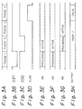
- Figures 3A to 3H are timing charts showing an operation of the bit field logic operation unit shown in Fig. 2.
- Fig. 3A represents four phases which constitute a machine cycle.
- Figs. 3B to 3D show waveforms of the CLK1 ⁇ , CLK2 ⁇ , and CLK0, respectively, shown in Fig. 2.
- Fig. 3E, Fig. 3F, and Fig. 3G represent operation modes of the logic operation part 38, the mask pattern generation part 40, and the bit map operation part 42.
- Fig. 3H represents a state of the output signal S.
- both the logic operation part 38 and the mask pattern generation part 40 are in the preset period, as the CLK1 ⁇ supplied to both parts is at "low" level (Fig. 3B) in phase 1.
- Potentials of circuit nodes in the logic operation part 38 are preset and potentials of circuit nodes in the mask pattern generation part 40 are preset at the same time.
- both the logic operation part 38 and the mask pattern generation part 40 are in the active period, as the CLK1 ⁇ is at "high” level.
- the logic operation part 38 outputs E according to the input A, B and F, and the mask pattern generation part 40 outputs MPG according to the input D and M.
- the bit map operation part 42 is in the preset period, as the CLK2 ⁇ is at "low” level in phase 2. Therefore, potentials of circuit nodes in the bit map operation part 42 are preset.
- phase 3 the bit map operation part 42 is in the active period, as the CLK2 ⁇ is at "high” level. Therefore the operation result is fixed within the bit map operation part 42 according to the E, MPG and B.
- phase 4 the output of the latch circuit 44 (Fig. 2) comprised in the bit map operation part 42 is valid as the CLK0 is at "high” level, so that the latch circuit 44 outputs the output signal S.
- Figure 4 shows a detailed construction of the mask pattern generation part 40.
- the mask data input size M represents a data type as shown in Table I.
- Table I M 1 M 0 data type MPG 0 -MPG 7 MPG 8 -MPG 15 MPG 16 -MPG 23 MPG 24 -MPG 31 0 0 byte x 1 1 1 0 1 half byte x x 1 1 1 0 word x x x x 1: all 1 X: determined by D
- MPG 8 - MPG 31 the upper 24 bits of MPG (MPG 8 - MPG 31 ) are forced to be "1" and the lower 8 bits of MPG are determined by the mask data D.
- the mask data D specifies a bit position which defines the most significant bit of bits having value of "0" as shown in Table II.
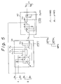
- Figure 5 shows detailed constructions of the logic operation part 38 and the bit map operation part 42.
- the least significant bits A 0 , B 0 , MPG 0 , and S 0
- Portions for other bits A 1-31 , B 1-31 , MPG 1-31 , and S 1-31 ) are identical.
- the logic operation part 38 performs a logic operation specified by the F 0 to F 3 on the source data A and the destination data B, and outputs E, as shown in Table III.
- Table III F 3 F 2 F 1 F 0 E 0 0 0 0 0 0 0 0 1 B ⁇ AND A ⁇ 0 0 1 1 A ⁇ 0 1 0 0 B ⁇ AND A 0 1 0 1 B ⁇ 0 1 1 0 B XOR A 0 1 1 1 B ⁇ OR A ⁇ 1 0 0 0 B AND A 1 0 0 1 B ⁇ XOR A 1 0 1 0 0 0 B AND A 1 0 0 1 B ⁇ XOR A 1 0 1 0 B 1 0 1 1 B OR A ⁇ 1 1 0 1 0 B 1 0 1 1 B OR A ⁇ 1 1 1 0 0 1 ⁇ OR A 1 1 1 1 1 0 B OR A ⁇ 1 1 0 0 1 0 1 1 B OR
- Figure 6 shows another embodiment of the bit map operation part 42.
- the signals U, L and N are signals for specifying a masking mode.
- a bit or bits of output signal S corresponding to a bit or bits of MPG having a logic value "1” become corresponding bit or bits of E
- a bit or bits of output signal S corresponding to a bit or bits of MPG having a logic value "0” become corresponding bit or bits of B, namely, the upper bit or bits are unmasked.
- the signal L is "1”
- a lower bit or bits are unmasked.
- the signal N is "1" all bits are unmasked.
Landscapes
- Engineering & Computer Science (AREA)
- Theoretical Computer Science (AREA)
- Software Systems (AREA)
- Physics & Mathematics (AREA)
- General Engineering & Computer Science (AREA)
- General Physics & Mathematics (AREA)
- Mathematical Physics (AREA)
- Executing Machine-Instructions (AREA)
- Image Processing (AREA)
Claims (9)
- Unité d'exécution d'opérations logiques sur zones binaires, comprenant :un moyen (38) d'exécution d'opérations logiques servant à effectuer une opération logique spécifiée sur des données de source (A) et des données de destination (B) afin de délivrer un résultat d'opération logique (E);un moyen (40) générateur de configurations de masquage servant à produire simultanément une configuration de masquage de bits (MPG) à partir d'une information de masquage (D, M) en parallèle avec le fonctionnement du moyen (38) d'exécution d'opérations logiques ; etun moyen (42) d'exécution d'opérations en grille de points servant à sélectionner soit le résultat d'opération logique (E), soit la donnée de destination (B) dans chaque position binaire en fonction de la configuration de masquage de bits (MPG) afin de délivrer un résultat d'opération logique masquée (S),caractérisée en ce que le moyen (38) d'exécutions d'opération logiques et le moyen (40) générateur de configurations de masquage sont constitués par des structures de circuits dynamiques où les traitements sont effectués dans une période de prépositionnement afin de prépositionner des potentiels de noeuds de circuit et une période active afin de délivrer des données traitées en fonction de signaux d'entrée, la période de prépositionnement et la période active du moyen (38) d'exécution d'opérations logiques chevauchent respectivement la période de prépositionnement et la période active du moyen (40) générateur de configurations de masquage, et en ce que les périodes actives du moyen (38) d'exécution d'opérations logiques et du moyen (40) générateur de configurations de masquage chevauchent la période de prépositionnement du moyen (42) d'exécution d'opérations en grille de points.
- Unité d'exécution d'opérations logiques sur zones binaires selon la revendication 1, où la période de prépositionnement du moyen d'exécution d'opérations logiques et la période de prépositionnement du moyen générateur de configurations de masquage s'effectuent simultanément.
- Unité d'exécution d'opérations logiques sur zones binaires selon la revendication 2, où le moyen d'exécution d'opérations sur grille de points est également constitué dans la structure de circuit dynamique.
- Unité d'exécution d'opération logique sur zones binaires selon la revendication 3, où la période active du moyen (38) d'exécution d'opérations logiques et du moyen (40) générateur de configurations de masquage et la période de prépositionnement du moyen (42) d'exécution d'opérations sur grille de points s'effectuent simultanément.
- Unité d'exécution d'opération logique sur zones binaires selon la revendication 4, où des signaux (U, L, N) servant à spécifier un mode de masquage sont appliqués à l'entrée du moyen (42') d'exécution d'opérations sur grille de points et un mode de fonctionnement du moyen (42') d'exécution d'opérations en grille de points est modifié en fonction des signaux.
- Microprocesseur monolithique comprenant :un moyen (10, 16) de réception d'instructions servant à recevoir une instruction ;un moyen de commande (18) servant à produire des signaux de commande en fonction de l'instruction transmise depuis le moyen de réception d'instruction (10, 16);une unité arithmétique et logique (26) servant à exécuter une opération arithmétique et logique en réponse aux signaux de commande ; etune unité (28) d'exécution d'opération logique sur zones binaires, connectée au moyen de commande (18) et servant à exécuter une opération logique sur des zones binaires de parties d'une donnée de source (A) et d'une donnée de destination (B) qui, toutes deux, comprennent une pluralité de bits, en réponse à une instruction de manipulation de bits, où l'unité (28) d'exécution d'opération logique sur zones binaires comprend :caractérisé en ce que le moyen (38) d'exécution d'opération logique, le moyen (40) générateur de configurations de masquage et le moyen (42) d'exécution d'opérations en grille de points sont constitués par des structures de circuits dynamiques, où les traitements sont effectués dans une période de prépositionnement afin de prépositionner un potentiel de noeuds de circuit et une période active afin de délivrer des données traitées en fonction de signaux d'entrée ; la période de prépositionnement et la période active du moyen d'exécution d'opérations logiques (38) chevauchent respectivement la période de prépositionnement et la période active du moyen générateur de configuration de masquage (40), et en ce que les périodes actives du moyen d'exécution d'opérations logiques (38) et du moyen générateur de configurations de masquage (40) chevauchent la période de prépositionnement du moyen d'exécution d'opérations en grille de points (42).un moyen (38) d'exécution d'opérations logiques servant à exécuter une opération logique spécifiée sur une donnée de source (A) et une donnée de destination (B) afin de délivrer un résultat d'opération logique (E);un moyen (40) générateur de configurations de masquage servant à produire simultanément une configuration de masquage de bits (MPG) à partir d'une information de masquage (D, M) en parallèle avec le fonctionnement du moyen (38) d'exécution d'opérations logiques ; etun moyen (42) d'exécution d'opérations en grille de points servant à sélectionner le résultat d'opération logique (E) ou bien la donnée de destination (B) dans chaque position binaire en fonction de la configuration de masquage de bits (MPG) afin de délivrer un résultat d'opération logique masquée (S),
- Microprocesseur monolithique selon la revendication 6, où le moyen générateur de configurations de masquage (40) reçoit une donnée de masquage (D) et une donnée de taille (M) et produit la configuration de masquage de bits (MPG) pour une zone binaire de longueur variable qui est spécifiée par les instructions de manipulation de bits.
- Microprocesseur monolithique selon la revendication 6, où l'unité arithmétique et logique (26) exécute des opérations excepté pour l'instruction de manipulation de bits.
- Microprocesseur monolithique selon la revendication 6, comprenant en outre un moyen qui forme un bus (32,34,36) connecté à l'unité d'exécution d'opération logique sur zones binaires (28) et à l'unité arithmétique et logique (26), où la donnée de source (A), la donnée de destination (B) et le résultat de l'opération logique masquée (S) sont transmis via le moyen formant un bus (32, 34, 36).
Applications Claiming Priority (2)
| Application Number | Priority Date | Filing Date | Title |
|---|---|---|---|
| JP178930/89 | 1989-07-13 | ||
| JP17893089 | 1989-07-13 |
Publications (3)
| Publication Number | Publication Date |
|---|---|
| EP0408464A2 EP0408464A2 (fr) | 1991-01-16 |
| EP0408464A3 EP0408464A3 (en) | 1992-08-19 |
| EP0408464B1 true EP0408464B1 (fr) | 1996-09-18 |
Family
ID=16057128
Family Applications (1)
| Application Number | Title | Priority Date | Filing Date |
|---|---|---|---|
| EP90402037A Expired - Lifetime EP0408464B1 (fr) | 1989-07-13 | 1990-07-13 | Unité pour des opérations logiques sur zones binaires et microprocesseur en comprenant ladite unité |
Country Status (5)
| Country | Link |
|---|---|
| US (1) | US5457803A (fr) |
| EP (1) | EP0408464B1 (fr) |
| JP (1) | JP2567134B2 (fr) |
| KR (1) | KR930009632B1 (fr) |
| DE (1) | DE69028583D1 (fr) |
Families Citing this family (5)
| Publication number | Priority date | Publication date | Assignee | Title |
|---|---|---|---|---|
| IT1247640B (it) * | 1990-04-26 | 1994-12-28 | St Microelectronics Srl | Operazioni booleane tra due qualsiasi bit di due qualsiasi registri |
| JP3433588B2 (ja) * | 1995-10-19 | 2003-08-04 | 株式会社デンソー | マスクデータ生成回路及びビットフィールド操作回路 |
| JP3560596B2 (ja) | 2002-08-22 | 2004-09-02 | 沖電気工業株式会社 | 演算装置及びデータの読出方法 |
| CN107967149B (zh) | 2011-12-23 | 2021-12-10 | 英特尔公司 | 从源写掩码寄存器在目的地写掩码寄存器中设置输出掩码的系统、装置和方法 |
| KR102075260B1 (ko) | 2018-08-07 | 2020-02-07 | 김윤식 | 마늘 분쇄기 |
Family Cites Families (4)
| Publication number | Priority date | Publication date | Assignee | Title |
|---|---|---|---|---|
| US4400794A (en) * | 1981-11-17 | 1983-08-23 | Burroughs Corporation | Memory mapping unit |
| US4785393A (en) * | 1984-07-09 | 1988-11-15 | Advanced Micro Devices, Inc. | 32-Bit extended function arithmetic-logic unit on a single chip |
| JPS61262923A (ja) * | 1985-05-17 | 1986-11-20 | Sharp Corp | パイプライン方式デ−タ処理回路の先まわり制御回路 |
| JP2583525B2 (ja) * | 1987-09-30 | 1997-02-19 | 健 坂村 | データ処理装置 |
-
1990
- 1990-07-13 KR KR1019900010655A patent/KR930009632B1/ko not_active Expired - Fee Related
- 1990-07-13 DE DE69028583T patent/DE69028583D1/de not_active Expired - Lifetime
- 1990-07-13 EP EP90402037A patent/EP0408464B1/fr not_active Expired - Lifetime
- 1990-07-13 JP JP2184088A patent/JP2567134B2/ja not_active Expired - Fee Related
-
1994
- 1994-02-28 US US08/202,876 patent/US5457803A/en not_active Expired - Fee Related
Also Published As
| Publication number | Publication date |
|---|---|
| KR910003941A (ko) | 1991-02-28 |
| EP0408464A3 (en) | 1992-08-19 |
| DE69028583D1 (de) | 1996-10-24 |
| JP2567134B2 (ja) | 1996-12-25 |
| EP0408464A2 (fr) | 1991-01-16 |
| US5457803A (en) | 1995-10-10 |
| JPH03129425A (ja) | 1991-06-03 |
| KR930009632B1 (ko) | 1993-10-08 |
Similar Documents
| Publication | Publication Date | Title |
|---|---|---|
| US10719318B2 (en) | Processor | |
| KR100266337B1 (ko) | 정보처리회로,반도체집적회로장치,마이크로컴퓨터,및전자기기 | |
| US5680597A (en) | System with flexible local control for modifying same instruction partially in different processor of a SIMD computer system to execute dissimilar sequences of instructions | |
| JP3592230B2 (ja) | データ処理装置 | |
| JP3954171B2 (ja) | コンピュータにおけるスカラ値をベクトルに記入する方法 | |
| EP1570373A1 (fr) | Moteur cellulaire pour un systeme informatique | |
| JPH0470662B2 (fr) | ||
| JPH07152733A (ja) | ベクトル・データを処理するコンピュータ・システムおよび方法 | |
| JP2622612B2 (ja) | 集積回路 | |
| US5666510A (en) | Data processing device having an expandable address space | |
| JP2023525811A (ja) | 行列処理のための可変位置シフト | |
| EP1680735B1 (fr) | Appareil et methode permettant d'utiliser de multiples jeux d'instructions et de multiples modes de decodage | |
| US5757685A (en) | Data processing system capable of processing long word data | |
| JPH11272546A (ja) | 可変長レジスタ装置 | |
| EP0408464B1 (fr) | Unité pour des opérations logiques sur zones binaires et microprocesseur en comprenant ladite unité | |
| EP0913764B1 (fr) | Méthode et appareil pour le décalage de données | |
| US5363322A (en) | Data processor with an integer multiplication function on a fractional multiplier | |
| KR19990037572A (ko) | 뱅크 어드레스 값을 공급하는 다중 소스를 구비하는 프로세서구조 설계 및 그 설계방법 | |
| US4691282A (en) | 16-bit microprocessor system | |
| US6975250B2 (en) | Methods and systems for data manipulation | |
| CA1321653C (fr) | Circuit de branchement prioritaire programmable | |
| JP2003241960A (ja) | プロセッサ、該プロセッサにおける演算命令処理方法及び演算制御方法 | |
| CN113853591A (zh) | 将预定义填补值插入到向量流中 | |
| JP2565495B2 (ja) | デ−タ処理システム | |
| JPH0685147B2 (ja) | 半導体回路装置 |
Legal Events
| Date | Code | Title | Description |
|---|---|---|---|
| PUAI | Public reference made under article 153(3) epc to a published international application that has entered the european phase |
Free format text: ORIGINAL CODE: 0009012 |
|
| AK | Designated contracting states |
Kind code of ref document: A2 Designated state(s): DE FR GB |
|
| PUAL | Search report despatched |
Free format text: ORIGINAL CODE: 0009013 |
|
| AK | Designated contracting states |
Kind code of ref document: A3 Designated state(s): DE FR GB |
|
| 17P | Request for examination filed |
Effective date: 19930127 |
|
| 17Q | First examination report despatched |
Effective date: 19951004 |
|
| GRAH | Despatch of communication of intention to grant a patent |
Free format text: ORIGINAL CODE: EPIDOS IGRA |
|
| GRAH | Despatch of communication of intention to grant a patent |
Free format text: ORIGINAL CODE: EPIDOS IGRA |
|
| GRAA | (expected) grant |
Free format text: ORIGINAL CODE: 0009210 |
|
| AK | Designated contracting states |
Kind code of ref document: B1 Designated state(s): DE FR GB |
|
| PG25 | Lapsed in a contracting state [announced via postgrant information from national office to epo] |
Ref country code: FR Effective date: 19960918 |
|
| REF | Corresponds to: |
Ref document number: 69028583 Country of ref document: DE Date of ref document: 19961024 |
|
| PG25 | Lapsed in a contracting state [announced via postgrant information from national office to epo] |
Ref country code: DE Effective date: 19961219 |
|
| EN | Fr: translation not filed | ||
| PLBE | No opposition filed within time limit |
Free format text: ORIGINAL CODE: 0009261 |
|
| STAA | Information on the status of an ep patent application or granted ep patent |
Free format text: STATUS: NO OPPOSITION FILED WITHIN TIME LIMIT |
|
| 26N | No opposition filed | ||
| REG | Reference to a national code |
Ref country code: GB Ref legal event code: IF02 |
|
| PGFP | Annual fee paid to national office [announced via postgrant information from national office to epo] |
Ref country code: GB Payment date: 20060712 Year of fee payment: 17 |
|
| GBPC | Gb: european patent ceased through non-payment of renewal fee |
Effective date: 20070713 |
|
| PG25 | Lapsed in a contracting state [announced via postgrant information from national office to epo] |
Ref country code: GB Free format text: LAPSE BECAUSE OF NON-PAYMENT OF DUE FEES Effective date: 20070713 |