EP0406889A2 - Verfahren zur Herstellung einer Festkörperbildaufnahmeanordnung - Google Patents
Verfahren zur Herstellung einer Festkörperbildaufnahmeanordnung Download PDFInfo
- Publication number
- EP0406889A2 EP0406889A2 EP90112942A EP90112942A EP0406889A2 EP 0406889 A2 EP0406889 A2 EP 0406889A2 EP 90112942 A EP90112942 A EP 90112942A EP 90112942 A EP90112942 A EP 90112942A EP 0406889 A2 EP0406889 A2 EP 0406889A2
- Authority
- EP
- European Patent Office
- Prior art keywords
- charge transfer
- light
- region
- state imaging
- imaging device
- Prior art date
- Legal status (The legal status is an assumption and is not a legal conclusion. Google has not performed a legal analysis and makes no representation as to the accuracy of the status listed.)
- Granted
Links
Images


Classifications
-
- H—ELECTRICITY
- H10—SEMICONDUCTOR DEVICES; ELECTRIC SOLID-STATE DEVICES NOT OTHERWISE PROVIDED FOR
- H10D—INORGANIC ELECTRIC SEMICONDUCTOR DEVICES
- H10D84/00—Integrated devices formed in or on semiconductor substrates that comprise only semiconducting layers, e.g. on Si wafers or on GaAs-on-Si wafers
- H10D84/01—Manufacture or treatment
- H10D84/0198—Integrating together multiple components covered by H10D44/00, e.g. integrating charge coupled devices
-
- H—ELECTRICITY
- H10—SEMICONDUCTOR DEVICES; ELECTRIC SOLID-STATE DEVICES NOT OTHERWISE PROVIDED FOR
- H10D—INORGANIC ELECTRIC SEMICONDUCTOR DEVICES
- H10D84/00—Integrated devices formed in or on semiconductor substrates that comprise only semiconducting layers, e.g. on Si wafers or on GaAs-on-Si wafers
- H10D84/01—Manufacture or treatment
- H10D84/02—Manufacture or treatment characterised by using material-based technologies
- H10D84/03—Manufacture or treatment characterised by using material-based technologies using Group IV technology, e.g. silicon technology or silicon-carbide [SiC] technology
- H10D84/038—Manufacture or treatment characterised by using material-based technologies using Group IV technology, e.g. silicon technology or silicon-carbide [SiC] technology using silicon technology, e.g. SiGe
-
- H—ELECTRICITY
- H10—SEMICONDUCTOR DEVICES; ELECTRIC SOLID-STATE DEVICES NOT OTHERWISE PROVIDED FOR
- H10F—INORGANIC SEMICONDUCTOR DEVICES SENSITIVE TO INFRARED RADIATION, LIGHT, ELECTROMAGNETIC RADIATION OF SHORTER WAVELENGTH OR CORPUSCULAR RADIATION
- H10F39/00—Integrated devices, or assemblies of multiple devices, comprising at least one element covered by group H10F30/00, e.g. radiation detectors comprising photodiode arrays
- H10F39/10—Integrated devices
- H10F39/12—Image sensors
- H10F39/15—Charge-coupled device [CCD] image sensors
Definitions
- the present invention relates to a solid-state imaging device and a method of manufacturing the same.
- a specific region of a semiconductor substrate (hereinafter abbreviated to substrate) 21 is implanted with an impurity of the same conductivity type as that of the substrate 21 to form an impurity region 22 that will isolate elements.
- substrate 21 is implanted with an impurity of the same conductivity type as that of the substrate 21 to form an impurity region 22 that will isolate elements.
- a light-sensitive element region 23 and a charge transfer region 24 are separately formed in specific regions of the substrate 21.
- a channel region 25 implanted with a specific impurity is formed in the region of the substrate 21 between the regions 23 and 24.
- the structure of this channel region 25 is such that it determines the characteristics of a transistor formed by the substrate 21, regions 23 and 24, and an electrode 27a (described below).
- an oxidation film 26a has been formed over the entire surface, a low-resistance polysilicon to which an impurity has been added is deposited thereon, and electrodes 27a and 27b are formed in the polysilicon by patterning. Subsequently, an insulation oxidation film 26b is formed over the top and sides of the low-resistance polysilicon by thermal oxidation.
- Low-resistance polysilicon is then deposited and patterned to form electrodes 28a and 28b.
- an insulating film 29 of, for instance, PSG is formed thickly over the entire surface by a vapor growth method, a light-proof film consisting of aluminum is deposited thereon. Part of the light-proof film corresponding to the light-sensitive element region 23 is removed by patterning, exposing a hole portion corresponding to the light-sensitive element region 23 while leaving light-proof films 30a and 30b on the insulating film 29, covering the regions outside the portion corresponding to the light-sensitive element region 23.
- the above conventional solid-state imaging device has the following problems:
- the present invention is designed to solve the above problems. It provides a solid-state imaging device that is both capable of high-speed operation and prevents the occurrence of smear noise, as far as is possible, and a manufacturing method that can produce such a solid-state imaging device.
- a method of manufacturing a solid-state imaging device which comprises the steps of: forming a light-sensitive element region and a charge transfer region that are isolated from each other, by implanting into specific regions of a semiconductor device of a first conductivity type an impurity of a second conductivity type, and, in addition, forming a channel region by implanting an impurity of said first conductivity type into a region of said semiconductor substrate between said light-sensitive element region and said charge transfer region; forming an insulation film over the entire surface of said semiconductor substrate; forming first charge transfer electrodes by depositing a film including at least an alloy consisting of a high-melting-point metal and silicon over said insulating film formed on said semiconductor substrate, patterning said film of alloy, then subjecting said alloy to high-temperature processing in a specific atmosphere; and forming second charge transfer electrodes by depositing a film including at least an alloy consisting of a high-melting-point metal and silicon over said first charge transfer electrodes formed on said semiconductor substrate, patterning
- a solid-state imaging device which comprises: a solid-state imaging device having: a light-sensitive element region and a charge transfer region formed by implanting into specific regions of a semiconductor substrate of a first conductivity type an impurity of a second conductivity type, said light-sensitive element region and said charge transfer region being isolated from each other; a channel region formed by implanting an impurity of said first conductivity type between said light-sensitive element region and said charge transfer region; and charge transfer electrodes formed of a light-proof material including at least an alloy consisting of a high-melting point metal and silicon on said channel region and said charge transfer region, with an inter-layer insulating material thereunder.
- first charge transfer electrodes are formed by subjecting the patterned film including at least the alloy of the high-melting-point metal and silicon to high-temperature processing in a specific atmosphere to turn into a silicide, then the top and sides of the film of the silicide of the high-melting-point metal are covered by an inter-layer insulating film made of SiO2. The same process is repeated to form second charge transfer electrodes.
- the electrodes formed in this way have a lower resistance and are impermeable to visible light, so the electrodes enable faster operation than conventional electrodes and, since the electrodes themselves act as a light-proof film, the electrodes can prevent the occurrence of smear noise, as far as is possible.
- the SiO2 inter-layer insulation film between the first and second charge transfer electrodes, consisting of the alloy of a high melting point metal and silicon has a two-layer structure, it is more stable than the conventional equivalent, so controllability of the solid-state imaging device is better.
- the solid-state imaging device of the present invention it is possible to provide a highly efficient solid-state imaging device which can operate at high speeds and prevent the occurrence of smear noise, as far as is possible, and which is also extremely controllable.
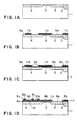
- Figs. 1A through 1D The process of manufacturing the solid-state imaging device of the present invention is shown in Figs. 1A through 1D.
- an impurity is implanted into specific regions of a semiconductor substrate (hereinafter abbreviated to substrate) 1 of a first conductivity type (for example, P-type) to form a light-sensitive element region 3 and a charge transfer region 4 of a second conductivity type (for example, N- type), and an impurity of the same conductivity type as the substrate 1 is implanted into the region surrounding the light-sensitive element region 3, except for a channel region 5 that will be described below, to form an element isolation region 2 to isolate adjacent elements.
- a specific impurity is implanted into the region of the substrate 1 between regions 3 and 4 to form the channel region 5 (see Fig. 1A).
- a film formed from an alloy of tungsten and silicon is deposited and patterned to form charge transfer electrodes 11a and 11b and a light-proof film 11c (see Fig. 1B).
- the charge transfer electrodes 11a and 11b and the light-proof film 11c formed of this tungsten-silicon alloy are then subjected to high-temperature processing in an atmosphere of O2 to turn the metal into its silicide, and an inter-layer insulation film 6b formed of SiO2 is grown up on the top and sides of the processed charge transfer electrodes 11a and 11b and the light-proof film 11c (see Fig. 1C).
- the component 11c on the element isolation region 2 is not used as an electrode; it functions as a light-proof film.
- Another film of tungsten-silicon alloy is then deposited and patterned to form a second layer of charge transfer electrodes 12a and 12b (see Fig. 1D).
- the second layer of charge transfer electrodes 12a and 12b is subjected to high-temperature processing in an atmosphere of O2 to turn the metal of the electrodes 12a and 12b into its silicide, and an inter-layer insulation film 6c formed of SiO2 is grown up on the top and sides of the processed charge transfer electrodes 12a and 12b, then the solid-state imaging device is completed by forming wiring.
- a protecting film could subsequently be formed over the entire surface.
- any high-melting-point metal silicide that has a low resistance and high heat tolerance can be used.
- a tungsten-silicon alloy in place of a tungsten-silicon alloy, a titanium-silicon, molybdenum-silicon alloy or tantalum-silicon alloy could be used.
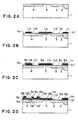
- the first layer of charge transfer electrodes 11a and 11b, and the second layer of charge transfer electrodes 12a and 12b are formed directly on top of the gate oxidation film 6a, but these layers could be formed by sequentially depositing and patterning a film for the electrode 11a of an alloy consisting of a high-melting-point metal (for example tungsten) and silicon, and a polysilicon film with an impurity on top of the gate oxidation film 6a, as shown in Figs. 2A-2D.
- an impurity is implanted to a predetermined region of the substrate 1 of the first conductivity type (for example, P-type) to form the light-sensitive element region 3 of the second conductivity type (for example, N-type) and the charge transfer region 4 of the second conductivity type, and the element isolation region 2, which is formed by implanting an impurity having the same conductivity type as the substrate 1, is formed at the surrounding region in the light-sensitive region except the channel region to isolate adjacent elements. Then the specific impurity is implanted into the region of the substrate 1 between regions 3 and 4 to form the channel region 5.
- the polysilicon film with the impurity and the film of the alloy consisting of tungsten and silicon are sequentially deposited and patterned to form the charge transfer electrodes 11a, 11a′, 11b and 11b′ and the light-proof films 11c and 11c′ (see Fig. 2B).
- the charge transfer electrodes 11a and 11b and the light-proof film 11c formed of the tungsten-silicon alloy are then subjected to high-temperature processing in an atmosphere of O2 to turn the metal into its silicide, and the inter-layer insulation film 6b formed of SiO2 is grown up on the top and sides of the processed charge transfer electrodes 11a, 11b and the light-proof film 11c and the polysilicon films of the charge transfer electrodes 11a′ and 11b′ and the sides of the polysilicon film of the light-proof film 11c′ (see Fig. 2C).
- the component 11c on the element isolation region 2 is not used as an electrode; it functions as a light-proof film.
- Another polysilicon film with the impurity and another film of tungsten-silicon alloy are then deposited and patterned to form the second layer of the charge transfer electrodes 12a, 12a′, 12b and 12b′ on the charge transfer electrodes 11a, 11a′, 11b and 11b′ (see Fig. 2D).
- the second layer of the charge transfer electrodes 12a and 12b is subjected to high-temperature processing in an atmosphere of O2 to turn the metal of the electrodes 12a and 12b into its silicide, and the inter-layer insulation film 6c formed of SiO2 is grown up on the top and sides of the processed charge transfer electrodes 12a and 12b, then the solid-state imaging device is completed by forming wiring.
- An additional protecting film can be formed over the entire device depending upon its uses.
- the light-sensitive element region 3 is formed before the charge transfer electrodes 11a, 11a′, 11b, 11b′, 12a, 12a′, 12b and 12b′ are formed, but it can also be formed by a self-alignment method after the charge transfer electrodes are formed.
- the individual charge transfer electrodes of the first layer are electrically connected to each other by the polysilicon, even if they should become damaged.
Landscapes
- Solid State Image Pick-Up Elements (AREA)
- Transforming Light Signals Into Electric Signals (AREA)
Applications Claiming Priority (4)
| Application Number | Priority Date | Filing Date | Title |
|---|---|---|---|
| JP175171/89 | 1989-07-06 | ||
| JP17517189 | 1989-07-06 | ||
| JP299251/89 | 1989-11-17 | ||
| JP1299251A JPH03129772A (ja) | 1989-07-06 | 1989-11-17 | 固体撮像装置およびその製造方法 |
Publications (3)
| Publication Number | Publication Date |
|---|---|
| EP0406889A2 true EP0406889A2 (de) | 1991-01-09 |
| EP0406889A3 EP0406889A3 (en) | 1991-12-11 |
| EP0406889B1 EP0406889B1 (de) | 1997-04-23 |
Family
ID=26496522
Family Applications (1)
| Application Number | Title | Priority Date | Filing Date |
|---|---|---|---|
| EP90112942A Expired - Lifetime EP0406889B1 (de) | 1989-07-06 | 1990-07-06 | Verfahren zur Herstellung einer Festkörperbildaufnahmeanordnung |
Country Status (2)
| Country | Link |
|---|---|
| EP (1) | EP0406889B1 (de) |
| DE (1) | DE69030533T2 (de) |
Family Cites Families (1)
| Publication number | Priority date | Publication date | Assignee | Title |
|---|---|---|---|---|
| EP0309542A1 (de) * | 1987-03-30 | 1989-04-05 | EASTMAN KODAK COMPANY (a New Jersey corporation) | Ladungsgekoppelte anordnung mit zweischichtigen elektroden |
-
1990
- 1990-07-06 DE DE69030533T patent/DE69030533T2/de not_active Expired - Fee Related
- 1990-07-06 EP EP90112942A patent/EP0406889B1/de not_active Expired - Lifetime
Also Published As
| Publication number | Publication date |
|---|---|
| EP0406889A3 (en) | 1991-12-11 |
| DE69030533D1 (de) | 1997-05-28 |
| DE69030533T2 (de) | 1997-09-18 |
| EP0406889B1 (de) | 1997-04-23 |
Similar Documents
| Publication | Publication Date | Title |
|---|---|---|
| US4102733A (en) | Two and three mask process for IGFET fabrication | |
| US4505027A (en) | Method of making MOS device using metal silicides or polysilicon for gates and impurity source for active regions | |
| US5466638A (en) | Method of manufacturing a metal interconnect with high resistance to electromigration | |
| US5395787A (en) | Method of manufacturing shallow junction field effect transistor | |
| NL8701251A (nl) | Halfgeleiderinrichting en werkwijze ter vervaardiging daarvan. | |
| JP3048459B2 (ja) | 半導体装置およびその製造方法 | |
| US5432363A (en) | Solid-state image pickup device and manufacturing method of the same | |
| JP2891237B2 (ja) | Soi構造の半導体装置およびその製造方法 | |
| JPS62162362A (ja) | Mos型集積回路及びその製造方法 | |
| US4729969A (en) | Method for forming silicide electrode in semiconductor device | |
| US6215142B1 (en) | Analog semiconductor device and method of fabricating the same | |
| US4076557A (en) | Method for providing semiconductor devices | |
| US5286669A (en) | Solid-state imaging device and method of manufacturing the same | |
| EP2842164B1 (de) | Halbleiterbauelement und verfahren zu seiner herstellung | |
| US5567641A (en) | Method of making a bipolar gate charge coupled device with clocked virtual phase | |
| JP2910839B2 (ja) | 半導体装置とその製造方法 | |
| US4954871A (en) | Semiconductor device with composite electrode | |
| EP0406889B1 (de) | Verfahren zur Herstellung einer Festkörperbildaufnahmeanordnung | |
| JPH02192161A (ja) | 半導体集積回路装置 | |
| KR930009142B1 (ko) | 고체촬상장치 및 그 제조방법 | |
| JPS58215055A (ja) | 半導体集積回路装置 | |
| JP2798289B2 (ja) | 電荷転送素子およびその製造方法 | |
| JP3176300B2 (ja) | 固体撮像装置及びその製造方法 | |
| JP2723854B2 (ja) | 固体撮像装置及びその製造方法 | |
| EP0035690A2 (de) | Halbleitervorrichtung mit isolierten Bauelementen und Verfahren zu ihrer Herstellung |
Legal Events
| Date | Code | Title | Description |
|---|---|---|---|
| PUAI | Public reference made under article 153(3) epc to a published international application that has entered the european phase |
Free format text: ORIGINAL CODE: 0009012 |
|
| 17P | Request for examination filed |
Effective date: 19900706 |
|
| AK | Designated contracting states |
Kind code of ref document: A2 Designated state(s): DE FR GB |
|
| PUAL | Search report despatched |
Free format text: ORIGINAL CODE: 0009013 |
|
| AK | Designated contracting states |
Kind code of ref document: A3 Designated state(s): DE FR GB |
|
| 17Q | First examination report despatched |
Effective date: 19931223 |
|
| GRAG | Despatch of communication of intention to grant |
Free format text: ORIGINAL CODE: EPIDOS AGRA |
|
| GRAG | Despatch of communication of intention to grant |
Free format text: ORIGINAL CODE: EPIDOS AGRA |
|
| GRAH | Despatch of communication of intention to grant a patent |
Free format text: ORIGINAL CODE: EPIDOS IGRA |
|
| GRAH | Despatch of communication of intention to grant a patent |
Free format text: ORIGINAL CODE: EPIDOS IGRA |
|
| GRAA | (expected) grant |
Free format text: ORIGINAL CODE: 0009210 |
|
| AK | Designated contracting states |
Kind code of ref document: B1 Designated state(s): DE FR GB |
|
| REF | Corresponds to: |
Ref document number: 69030533 Country of ref document: DE Date of ref document: 19970528 |
|
| ET | Fr: translation filed | ||
| PLBE | No opposition filed within time limit |
Free format text: ORIGINAL CODE: 0009261 |
|
| STAA | Information on the status of an ep patent application or granted ep patent |
Free format text: STATUS: NO OPPOSITION FILED WITHIN TIME LIMIT |
|
| 26N | No opposition filed | ||
| REG | Reference to a national code |
Ref country code: GB Ref legal event code: 746 Effective date: 19981015 |
|
| REG | Reference to a national code |
Ref country code: FR Ref legal event code: D6 |
|
| REG | Reference to a national code |
Ref country code: GB Ref legal event code: IF02 |
|
| PGFP | Annual fee paid to national office [announced via postgrant information from national office to epo] |
Ref country code: DE Payment date: 20070628 Year of fee payment: 18 |
|
| PGFP | Annual fee paid to national office [announced via postgrant information from national office to epo] |
Ref country code: GB Payment date: 20070704 Year of fee payment: 18 |
|
| PGFP | Annual fee paid to national office [announced via postgrant information from national office to epo] |
Ref country code: FR Payment date: 20070710 Year of fee payment: 18 |
|
| GBPC | Gb: european patent ceased through non-payment of renewal fee |
Effective date: 20080706 |
|
| PG25 | Lapsed in a contracting state [announced via postgrant information from national office to epo] |
Ref country code: DE Free format text: LAPSE BECAUSE OF NON-PAYMENT OF DUE FEES Effective date: 20090203 |
|
| REG | Reference to a national code |
Ref country code: FR Ref legal event code: ST Effective date: 20090331 |
|
| PG25 | Lapsed in a contracting state [announced via postgrant information from national office to epo] |
Ref country code: GB Free format text: LAPSE BECAUSE OF NON-PAYMENT OF DUE FEES Effective date: 20080706 |
|
| PG25 | Lapsed in a contracting state [announced via postgrant information from national office to epo] |
Ref country code: FR Free format text: LAPSE BECAUSE OF NON-PAYMENT OF DUE FEES Effective date: 20080731 |