EP0405877A2 - Transistor interdigité optimisé thermalement - Google Patents
Transistor interdigité optimisé thermalement Download PDFInfo
- Publication number
- EP0405877A2 EP0405877A2 EP90306902A EP90306902A EP0405877A2 EP 0405877 A2 EP0405877 A2 EP 0405877A2 EP 90306902 A EP90306902 A EP 90306902A EP 90306902 A EP90306902 A EP 90306902A EP 0405877 A2 EP0405877 A2 EP 0405877A2
- Authority
- EP
- European Patent Office
- Prior art keywords
- heat
- transistor
- regions
- generating
- region
- Prior art date
- Legal status (The legal status is an assumption and is not a legal conclusion. Google has not performed a legal analysis and makes no representation as to the accuracy of the status listed.)
- Granted
Links
Images

Classifications
-
- H10W40/22—
-
- H—ELECTRICITY
- H10—SEMICONDUCTOR DEVICES; ELECTRIC SOLID-STATE DEVICES NOT OTHERWISE PROVIDED FOR
- H10D—INORGANIC ELECTRIC SEMICONDUCTOR DEVICES
- H10D30/00—Field-effect transistors [FET]
- H10D30/60—Insulated-gate field-effect transistors [IGFET]
-
- H—ELECTRICITY
- H10—SEMICONDUCTOR DEVICES; ELECTRIC SOLID-STATE DEVICES NOT OTHERWISE PROVIDED FOR
- H10D—INORGANIC ELECTRIC SEMICONDUCTOR DEVICES
- H10D62/00—Semiconductor bodies, or regions thereof, of devices having potential barriers
- H10D62/10—Shapes, relative sizes or dispositions of the regions of the semiconductor bodies; Shapes of the semiconductor bodies
- H10D62/124—Shapes, relative sizes or dispositions of the regions of semiconductor bodies or of junctions between the regions
- H10D62/126—Top-view geometrical layouts of the regions or the junctions
Definitions
- the present invention relates to the thermal optimization of transistors, and more particularly to a thermally optimized quasi-interdigitated radio frequency power transistor.
- Solid-state power amplifiers have received considerable attention since the invention of the solid-state transistor and the solid-state integrated circuit.
- Heat is generated in the active regions of field effect transistors (FETs) and bipolar junction transistors (BJTs) as a result of I2R losses. This heat affects the reliability and thus the mean time before failure (MTBF) of these transistors.
- FETs field effect transistors
- BJTs bipolar junction transistors
- MTBF mean time before failure
- the semiconductor chip in which a solid-state power amplifier is built is typically mounted on a metal or composite material having a thermal conductivity that is at least two times greater than the thermal conductivity of the semiconductor, k semi .
- k semi is generally the limiting component in heat dissipation from the power amplifier.
- the reference temperature, T0 is generally room temperature or, in degrees Kelvin, approximately 300K.
- the values for k0 are 1.45 ⁇ 0.05 and 0.44 ⁇ 0.04 W/cm-K, respectively.
- semiconductor impurity i.e. dopant
- concentrations exceed 1015 atoms/cm3
- thermal conductivity of the conducting medium is reduced. This results from photon-electron scattering.
- k semi will not degrade more than approximately 20% due to semiconductor impurities.
- T active the active temperature for semiconductor regions
- P Dmax the density of rf power generated by a power amplifier transistor
- rf power density has been increased while minimizing the overall chip width W by interdigitating small transistor sections or heat-generating regions. These transistor sections are placed as close as possible to each other while maintaining T active below an acceptable value during device operation.
- Another conventional approach is to use thinner semiconductor substrates. This increases the dT/dz, where z is in the direction of the substrate thickness, and causes increased heat transfer.
- certain other components such as distributed transmission lines fix lower limits on substrate thickness.
- an interdigitated transistor is provided that is formed at a face of a semiconductor layer.
- a plurality of subtransistors are formed at the face which have inputs connected in common and outputs connected in common, each subtransistor having a heat-generating region which generates heat during operation of the transistor.
- the heat-generating regions are disposed in a single row in an x-direction, but are offset from adjacent heat-generating regions in a y-direction. Therefore, the heat from each heat-generating region will dissipate by at least a predetermined desired amount independently from adjacent heat-generating regions, keeping the T active of the transistor within acceptable operating limits.
- each heat generating region which for example may be a channel region of a field effect transistor, has a center positioned on a V-shaped line such that more transistors including these sections may be fit within a predetermined cavity dimension (w) in the transverse direction that is less than half of the effective operating wavelength, thereby avoiding waveguide resonating mode problems.
- V-shaped arrangement of the channel regions with respect to one another can be outwardly curved.
- the transverse spacing between adjacent channel regions and the ends of the "V" are set at a predetermined distance to meet each region's dissipation requirements. As each branch of the "V" curves inwardly to a longitudinal axis of the transistor, the transverse spacing between adjacent channel sections can be decreased because of the increased offset.
- the V-shaped arrangement provides another technical advantage in that it provides an anti-symmetric combination of the signal from the various signal paths. Therefore, there is little or no phase cancellation experienced within the device and accordingly no loss of power for this reason as is usually experienced in conventional interdigitated transistors.
- the power transistor is a junction field effect transistor.
- a drain contact and a gate contact are positioned on a longitudinal axis.
- a pair of gate manifolds extend from the gate contact longitudinally toward the drain contact and transversely outward from the longitudinal axis.
- a plurality of channel regions are formed between the gate manifolds and the drain contact on the "V" shaped pattern as described above.
- Each of the gate regions has its electrical conductance controlled by a respective gate electrode that is conductively coupled to one of the gate manifolds.
- Each of the channel regions has associated with it a drain region that is preferably formed as a diffused finger that extends from the drain contact.
- a source region that is electrically coupled to one of two source contacts through a metal air bridge over one of the gate manifolds.
- the present invention provides significant technical advantages in that it affords a transistor design having a width or transverse dimension that is less smaller, but which at the same time increases the heat dissipation ability of the transistor while in operation and avoids losses due to phase cancellation from multiple parallel signal paths.
- the transistor of the invention may therefore be operated at higher power and higher rf frequencies, and more of the transistors may be fit onto a chip having a width w that is less than ⁇ /2.
- heat dissipation may be resolved into three vector components: x, y and z, corresponding to the axes of a typical three-dimensional coordinate system as shown in FIGURE 1.
- FIGURE 2 is a highly schematic isometric view of a interdigitated transistor according to the prior art.
- the transistor is formed at a face 10 of a semiconductor substrate or bulk semiconductor 12.
- the substrate 12 generally has a thickness in the z-direction that is much less than its length or width in the y or x-directions, respectively.
- the transistor comprises a plurality of heat-generating sections 14, which in the case of field-effect transistors are the channel regions disposed between neighboring source and drain regions (not shown).
- the principle of the invention is also applicable to bipolar devices, wherein the heat generating regions 14 would comprise entire bipolar devices.
- each of the heat-generating regions 14 will originate heat that is transferred in the x-, y- and z-directions.
- the vectors labeled q x , q y , and q z represent the heat transfer in these appropriate directions.
- the temperature differential in the z-direction, dT/dz, is greater than the temperature differential in the x- and y-directions, dT/dx and dT/dy, respectively.
- the thermal conductivity of the metal or composite mounting material may be considered infinite and at a constant temperature, T sink .
- the thickness z of the semiconductor substrate 12 and T active are fixed, the only possible way to reduce the spacing between adjacent transistor heat-generating sections 14 is to reduce the contribution of q x from neighboring transistor sections.
- FIGURE 3 a highly schematic isometric view of a quasi-interdigitated transistor according to the invention is shown. Like numbers identify like parts between FIGURES 2 and 3. As can be seen, the position of adjacent transistor sections 14 is shifted in the y-direction to reduce the contribution of q x from neighboring transistor sections 14. The partial removal of the q x component of heat from adjacent transistor sections 14 allows the interdigitated transistor to dissipate heat more efficiently, assuming all other factors to be the same, and therefore the transistor may be operated at a higher power and at lower or equal T active .
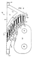
- FIGURE 4 is a highly magnified schematic plan view of a quasi-interdigitated transistor for use in microwave power applications. This transistor is indicated generally at 50, and is formed at a face of a semiconductor substrate 52. Only certain components of transistor 50 are shown in FIGURE 4 for the sake of clarity.
- Transistor 50 is a metal semiconductor field effect transistor (MESFET).
- a drain contact is indicated at 54. Connection is made to other amplifier components through the drain contact 54, a plurality of source vias 56 and a gate contact 58. Each of these contacts is made through a passivating dielectric layer (not shown) to the face of the semiconductor substrate 52.
- MESFET metal semiconductor field effect transistor
- the drain contact 54 is conductively connected to a metallized drain manifold, the outline of which is indicated at 60.
- the drain manifold 60 takes a hollow diamond-shaped pattern, and includes a pair of lower arms 62.
- a plurality of metallized drain contact fingers 64 extend from the lower drain manifold arm 62 longitudinally in the direction of the gate contact 58.
- Each of the drain contact fingers 64 makes connection to a respective drain region (not shown; see FIGURE 5) that is diffused into the semiconductor layer 52.
- the transistor 50 is provided with a plurality of channel regions 80.
- the channel regions 80 are the source of most of the heat generated during operation of the transistor 50, such that their locations may dictate the modelling of the entire device 50.
- Each of the channel regions 80 where for instance the substrate 52 is gallium arsenide, is an elongate rectangle of (N) type material between a respective drain region and a respective source region (both later described), with the length of each channel region 80 in a longitudinal or y-direction being much greater than its width in a transverse or x-direction. (In FIGURE 4, y is in a vertical direction, while x is in the horizontal direction).
- Each of the rectangular channel regions 80 is offset in a y-direction from the adjacent channel regions 80.
- Each of the channel regions 80 is connected through a metal conductor shown schematically at 82 to one of two metal arms 84 of a gate manifold indicated generally at 86.
- the gate manifold 86 is in turn connected to the gate contact 58.
- each source region 88 Disposed on one side of each of the channel regions 80 is a respective source region 88 (not shown; see FIGURE 5) .
- Each source region 88 is diffused into the semiconductor substrate 52 to be (N+), where the drain regions are also selected to be (N+).
- Each source region 88 is connected to one of two metal source contact pads 90 through a respective conductive air bridge 92 that is insulatively separated from the gate manifold arm 84 over which it passes by both a dielectric passivating layer (not shown) and air.
- a longitudinal one-half of the transistor 50 is shown in more detail in FIGURE 5.
- the y axis is indicated at 100, and only the right one-half of the transistor 50 is shown.
- Channel regions 102-118 are not offset by a constant amount as one proceeds transversely from the y axis 100. Instead, the longitudinal centers of the channel regions 102-118 fall on a curved V-shaped locus that extends from the y axis 100 in a longitudinal direction toward the drain contact 54, while progressively curving transversely. More inwardly disposed channel regions 102-108 are offset from each other in the y-direction by a fairly constant amount.
- the incremental offset of the more outer channel regions 110-118 from each other, and from channel region 108, begins to decrease as one proceeds in a transverse direction from the y-axis 100.
- This arcuate or serpentine positioning was optimized using a thermal modelling program incorporating a finite difference technique.
- Each of the channel regions 102-118 has a corresponding gate electrode 120-136 that is bonded directly to the surface of its respective channel region 102-118.
- each gate electrode 120-136 is recessed into the face of the semiconductor substrate 52. While each channel region is associated with only one gate electrode in the illustrated embodiment, the invention also applies to channel regions having multiple electrodes.
- the separation of the channel regions 102-118 in an x or transverse direction increases as one proceeds from the y-axis. This is because there is more y-offset between adjacent channel regions near the axis 100, and relatively less y-offset of adjacent channel regions further from the axis 300. Because of this, the heat component q x from any channel region adjacent to a channel region that is relatively removed from the axis 100 becomes a greater concern, and a further transverse spacing is required in comparison to those channel regions nearer the axis 100.
- the illustrated transistor 50 is preferably formed on a chip with several other like transistors in a single row in the x-direction.
- the chip width w must be kept less than the waveguide cutoff frequency, ⁇ /2, to prevent waveguide resonating modes and feedback of a portion of the rf energy to the inputs of the transistor 50.
- the arcuate ⁇ design of the transistor of the invention allows a sufficiently close spacing of adjacent channel regions 102-118 that a smaller w becomes possible for any particular power application. Meanwhile, thermal optimization has insured that a constant channel or junction temperature T active is maintained throughout all of the channel regions 102-118.
- Another advantage of the invention is its anti-symmetric combining structure.
- the signal appears at the gate contact 58, and is amplified by the various transistor sections to appear at the drain contact 54 through a plurality of multiple parallel paths. Each one of these multiple parallel paths has a propagation time delay associated with it. For example, in one path, the signal proceeds from the gate contact 58 to the gate manifold 86 and starts up the gate manifold arm 84. It proceeds up a gate conductor 122, where it is amplified with current supplied from a channel region 104. The amplified signal continues through drain region 148, and travels through an associated drain contact finger 150 to the drain contact arm 62 and from thence to the drain contact 54.
- the signal proceeds all the way up the gate contact manifold arm 84 to a gate conductor 118.
- the signal as amplified continues through at a drain region 152 and proceeds from thence to a drain finger 154 to the drain manifold 60 and the drain contact 54.
- a novel quasi-interdigitated transistor has been described, wherein multiple channel regions are offset from one another in reference to a particular axis to remove a portion of the heating experienced by adjacent channel regions.
- the transistor has been modelled to maintain a uniform T active for each channel region in the device, while at the same time having a transverse dimension that is less than the waveguide cutoff frequency.
- the transistor of the invention has the further advantage of equal time propagation delays associated with multiple signal paths.
Landscapes
- Junction Field-Effect Transistors (AREA)
- Bipolar Integrated Circuits (AREA)
- Bipolar Transistors (AREA)
Applications Claiming Priority (2)
| Application Number | Priority Date | Filing Date | Title |
|---|---|---|---|
| US37442289A | 1989-06-30 | 1989-06-30 | |
| US374422 | 1989-06-30 |
Publications (3)
| Publication Number | Publication Date |
|---|---|
| EP0405877A2 true EP0405877A2 (fr) | 1991-01-02 |
| EP0405877A3 EP0405877A3 (en) | 1991-06-26 |
| EP0405877B1 EP0405877B1 (fr) | 1994-03-16 |
Family
ID=23476747
Family Applications (1)
| Application Number | Title | Priority Date | Filing Date |
|---|---|---|---|
| EP90306902A Expired - Lifetime EP0405877B1 (fr) | 1989-06-30 | 1990-06-25 | Transistor interdigité optimisé thermalement |
Country Status (3)
| Country | Link |
|---|---|
| EP (1) | EP0405877B1 (fr) |
| JP (1) | JP2873049B2 (fr) |
| DE (1) | DE69007351T2 (fr) |
Cited By (3)
| Publication number | Priority date | Publication date | Assignee | Title |
|---|---|---|---|---|
| EP0560123A3 (en) * | 1992-03-12 | 1994-05-25 | Siemens Ag | Power transistor with multiple finger contacts |
| WO1999026294A1 (fr) * | 1997-11-13 | 1999-05-27 | Northrop Grumman Corporation | Transistor bipolaire a heterojonction pour circuit a micro-ondes a densite de puissance elevee a distribution des signaux uniforme |
| WO2001088980A1 (fr) * | 2000-05-17 | 2001-11-22 | Telefonaktiebolaget Lm Ericsson | Transistors de puissance destines a des radiofrequences |
Families Citing this family (1)
| Publication number | Priority date | Publication date | Assignee | Title |
|---|---|---|---|---|
| EP3474316B1 (fr) * | 2016-07-25 | 2021-03-03 | Mitsubishi Electric Corporation | Dispositif à semi-conducteurs |
Family Cites Families (1)
| Publication number | Priority date | Publication date | Assignee | Title |
|---|---|---|---|---|
| GB2175441B (en) * | 1985-05-03 | 1989-05-10 | Texas Instruments Ltd | Power bipolar transistor |
-
1990
- 1990-06-25 EP EP90306902A patent/EP0405877B1/fr not_active Expired - Lifetime
- 1990-06-25 DE DE69007351T patent/DE69007351T2/de not_active Expired - Fee Related
- 1990-06-29 JP JP2170437A patent/JP2873049B2/ja not_active Expired - Fee Related
Cited By (5)
| Publication number | Priority date | Publication date | Assignee | Title |
|---|---|---|---|---|
| EP0560123A3 (en) * | 1992-03-12 | 1994-05-25 | Siemens Ag | Power transistor with multiple finger contacts |
| WO1999026294A1 (fr) * | 1997-11-13 | 1999-05-27 | Northrop Grumman Corporation | Transistor bipolaire a heterojonction pour circuit a micro-ondes a densite de puissance elevee a distribution des signaux uniforme |
| US6034383A (en) * | 1997-11-13 | 2000-03-07 | Northrop Grumman Corporation | High power density microwave HBT with uniform signal distribution |
| WO2001088980A1 (fr) * | 2000-05-17 | 2001-11-22 | Telefonaktiebolaget Lm Ericsson | Transistors de puissance destines a des radiofrequences |
| US6507047B2 (en) | 2000-05-17 | 2003-01-14 | Telefonaktiebolaget Lm Ericsson (Publ) | Power transistors for radio frequencies |
Also Published As
| Publication number | Publication date |
|---|---|
| JPH03123035A (ja) | 1991-05-24 |
| DE69007351D1 (de) | 1994-04-21 |
| DE69007351T2 (de) | 1994-09-08 |
| EP0405877A3 (en) | 1991-06-26 |
| EP0405877B1 (fr) | 1994-03-16 |
| JP2873049B2 (ja) | 1999-03-24 |
Similar Documents
| Publication | Publication Date | Title |
|---|---|---|
| US6900482B2 (en) | Semiconductor device having divided active regions with comb-teeth electrodes thereon | |
| JP5095387B2 (ja) | 熱スペーサを有する半導体デバイス | |
| EP2941102B1 (fr) | Transfert thermique réduit vers des fet de peltier refroidis | |
| US6424006B1 (en) | Semiconductor component | |
| US9502330B1 (en) | Coolant distribution structure for monolithic microwave integrated circuits (MMICs) | |
| EP3497727B1 (fr) | Transistors de puissance | |
| US5708283A (en) | Flip chip high power monolithic integrated circuit thermal bumps | |
| US6507047B2 (en) | Power transistors for radio frequencies | |
| JP2016507889A (ja) | トランジスタ、トランジスタの放熱構造及びトランジスタの製造方法 | |
| EP4239672A1 (fr) | Dispositif semi-conducteur | |
| US5057882A (en) | Thermally optimized interdigitated transistor | |
| EP0405877B1 (fr) | Transistor interdigité optimisé thermalement | |
| CA2058672C (fr) | Dispositif a semi-conducteurs permettant d'ameliorer les caracteristiques haute frequence et d'eliminer le fendillement des microplaquettes | |
| US5311148A (en) | Thermally optimized interdigitated transistor | |
| US20200013692A1 (en) | Semiconductor power device including wire or ribbon bonds over device active region | |
| WO2000022666A2 (fr) | Procede et dispositif d'interconnexion pour transistors sic a effet de champ pour puissance haute frequence | |
| JP7294385B2 (ja) | 半導体増幅素子及び半導体増幅装置 | |
| JPH0645520A (ja) | パワートランジスタ | |
| US7919855B2 (en) | Topside thermal management of semiconductor devices using boron phosphide contacting a gate terminal | |
| McDonald et al. | Wafer scale interconnections for GaAs packaging-Applications to RISC architecture | |
| JPH10200312A (ja) | マイクロ波集積回路 | |
| JPH03142845A (ja) | 電界効果トランジスタ | |
| JPH0425031A (ja) | 高出力モノリシックマイクロ波集積回路 | |
| Bessemoulin et al. | Design of coplanar power amplifiers for millimeter-wave system applications including thermal aspects | |
| JPH04116836A (ja) | マイクロ波半導体装置 |
Legal Events
| Date | Code | Title | Description |
|---|---|---|---|
| PUAI | Public reference made under article 153(3) epc to a published international application that has entered the european phase |
Free format text: ORIGINAL CODE: 0009012 |
|
| AK | Designated contracting states |
Kind code of ref document: A2 Designated state(s): DE FR GB IT NL |
|
| PUAL | Search report despatched |
Free format text: ORIGINAL CODE: 0009013 |
|
| AK | Designated contracting states |
Kind code of ref document: A3 Designated state(s): DE FR GB IT NL |
|
| 17P | Request for examination filed |
Effective date: 19911219 |
|
| 17Q | First examination report despatched |
Effective date: 19920817 |
|
| GRAA | (expected) grant |
Free format text: ORIGINAL CODE: 0009210 |
|
| ITF | It: translation for a ep patent filed | ||
| AK | Designated contracting states |
Kind code of ref document: B1 Designated state(s): DE FR GB IT NL |
|
| REF | Corresponds to: |
Ref document number: 69007351 Country of ref document: DE Date of ref document: 19940421 |
|
| ET | Fr: translation filed | ||
| PLBE | No opposition filed within time limit |
Free format text: ORIGINAL CODE: 0009261 |
|
| STAA | Information on the status of an ep patent application or granted ep patent |
Free format text: STATUS: NO OPPOSITION FILED WITHIN TIME LIMIT |
|
| 26N | No opposition filed | ||
| ITTA | It: last paid annual fee | ||
| REG | Reference to a national code |
Ref country code: GB Ref legal event code: IF02 |
|
| PGFP | Annual fee paid to national office [announced via postgrant information from national office to epo] |
Ref country code: NL Payment date: 20070507 Year of fee payment: 18 |
|
| PGFP | Annual fee paid to national office [announced via postgrant information from national office to epo] |
Ref country code: DE Payment date: 20070629 Year of fee payment: 18 |
|
| PGFP | Annual fee paid to national office [announced via postgrant information from national office to epo] |
Ref country code: GB Payment date: 20070511 Year of fee payment: 18 |
|
| PGFP | Annual fee paid to national office [announced via postgrant information from national office to epo] |
Ref country code: IT Payment date: 20070628 Year of fee payment: 18 |
|
| PGFP | Annual fee paid to national office [announced via postgrant information from national office to epo] |
Ref country code: FR Payment date: 20070605 Year of fee payment: 18 |
|
| GBPC | Gb: european patent ceased through non-payment of renewal fee |
Effective date: 20080625 |
|
| NLV4 | Nl: lapsed or anulled due to non-payment of the annual fee |
Effective date: 20090101 |
|
| REG | Reference to a national code |
Ref country code: FR Ref legal event code: ST Effective date: 20090228 |
|
| PG25 | Lapsed in a contracting state [announced via postgrant information from national office to epo] |
Ref country code: DE Free format text: LAPSE BECAUSE OF NON-PAYMENT OF DUE FEES Effective date: 20090101 |
|
| PG25 | Lapsed in a contracting state [announced via postgrant information from national office to epo] |
Ref country code: NL Free format text: LAPSE BECAUSE OF NON-PAYMENT OF DUE FEES Effective date: 20090101 |
|
| PG25 | Lapsed in a contracting state [announced via postgrant information from national office to epo] |
Ref country code: GB Free format text: LAPSE BECAUSE OF NON-PAYMENT OF DUE FEES Effective date: 20080625 |
|
| PG25 | Lapsed in a contracting state [announced via postgrant information from national office to epo] |
Ref country code: FR Free format text: LAPSE BECAUSE OF NON-PAYMENT OF DUE FEES Effective date: 20080630 Ref country code: IT Free format text: LAPSE BECAUSE OF NON-PAYMENT OF DUE FEES Effective date: 20080625 |