EP0403147B1 - Leistungsschnittstellenschaltung und Verfahren zur Prüfung einer solchen Schaltung - Google Patents
Leistungsschnittstellenschaltung und Verfahren zur Prüfung einer solchen Schaltung Download PDFInfo
- Publication number
- EP0403147B1 EP0403147B1 EP90306136A EP90306136A EP0403147B1 EP 0403147 B1 EP0403147 B1 EP 0403147B1 EP 90306136 A EP90306136 A EP 90306136A EP 90306136 A EP90306136 A EP 90306136A EP 0403147 B1 EP0403147 B1 EP 0403147B1
- Authority
- EP
- European Patent Office
- Prior art keywords
- signal
- transmitter
- conductor
- receiver
- output
- Prior art date
- Legal status (The legal status is an assumption and is not a legal conclusion. Google has not performed a legal analysis and makes no representation as to the accuracy of the status listed.)
- Expired - Lifetime
Links
- 238000010998 test method Methods 0.000 title claims description 11
- 239000004020 conductor Substances 0.000 claims description 131
- 238000012360 testing method Methods 0.000 claims description 87
- 238000000034 method Methods 0.000 claims description 7
- 238000004519 manufacturing process Methods 0.000 claims description 4
- 238000012956 testing procedure Methods 0.000 claims description 4
- 238000010586 diagram Methods 0.000 description 5
- 238000013461 design Methods 0.000 description 3
- 238000012546 transfer Methods 0.000 description 3
- 238000001514 detection method Methods 0.000 description 1
- 230000008054 signal transmission Effects 0.000 description 1
Images


Classifications
-
- H—ELECTRICITY
- H04—ELECTRIC COMMUNICATION TECHNIQUE
- H04L—TRANSMISSION OF DIGITAL INFORMATION, e.g. TELEGRAPHIC COMMUNICATION
- H04L1/00—Arrangements for detecting or preventing errors in the information received
- H04L1/24—Testing correct operation
- H04L1/242—Testing correct operation by comparing a transmitted test signal with a locally generated replica
- H04L1/243—Testing correct operation by comparing a transmitted test signal with a locally generated replica at the transmitter, using a loop-back
Definitions
- This invention relates to line interface circuits and in particular to the testing of such circuits.
- Line interface circuits include the line drivers and receivers and are susceptible to failures such as the shorting together of two conductors within a cable or damage to the line driver or receiver as result of electrical overstress. It is therefore essential to be able to test line interface circuits to ensure their functionality.
- the common form of test is the loopback test, which is usually performed by removing the connection to the line from the interface and replacing it with another connector in which the driver or drivers in the interface are directly connected to an associated line receiver or receivers.
- data is sent from a line driver and its correct receipt by a receiver can be checked. Using this test, a fault can be traced to an individual driver/receiver pair or by deduction to a problem within the cable itself.
- European Patent Application No. 0 176 646 discloses a line interface circuit for connecting the transmit ports of a transmitter to transmit lines and the receive ports of the transmitter to receive lines, wherein switching means included in the line interface circuit makes it possible to use the line interface circuit either to drive the transmit line or to loop the output signal from the transmitter back to its input port, in order to perform a loopback test, while loading the transmit line with its characteristic impedance.
- the invention provides a line interface circuit comprising:
- said auxiliary output conductor means of said transmitter means comprises auxiliary first and second output conductors for respectively providing a test signal to said receiver means via said selective signal-applying means varying between first and second steady voltage levels each of which is restricted from crossing the threshold level.
- said means for selectively producing a test signal includes clamping means connected to said transmitter means for restricting the output signal of said transmitter means during a testing procedure to voltage levels respectively provided to said first and second auxiliary output conductors and of amplitude restricting the test signal from crossing the threshold level;
- said transmitter means includes
- resistive means are disposed between said first transistor and said first voltage supply conductor connected thereto; and the junction node between the resistive means and said first transistor is connected to said selective signal-applying means such that said selective signal-applying means can monitor the operational state of said first transistor.
- said selective signal-applying means comprises a cross-feed switch device alternately applying the test signals on said auxiliary first and second output conductors to the second input of said receiver means.
- said receiver means further includes a first stage having a transistor provided with a control component;
- said selective signal-applying means applies a switched current to the electrode region of the transistor included in the first stage of said receiver means.
- output and input signals applied to and received from the line are standardized signals.
- the invention provides a method of testing a line interface circuit having a transmitter and a receiver for sending and receiving a signal varying between a first voltage level and a second voltage level to and from respective conductors of the line, wherein the transmitter provides an output signal to a first conductor of the line and the receiver receives an input signal from a second conductor of the line, said method comprising the steps of:
- the test signal is provided as a small amplitude signal based upon one of the first and second voltage levels of the output signal.
- the method includes alternately applying the test signal from first and second auxiliary output conductors of the transmitter as a test signal varying between first and second steady voltage levels; and restricting each of the first and second voltage levels as provided by the auxiliary output conductors of the transmitter from crossing the threshold level as provided to said receiver.
- the method includes clamping the output signal of the transmitter during a testing procedure to voltage levels of amplitude restricting the test signal from crossing the threshold level.
- the method includes selectively applying an enabling signal to said transmitter for placing said transmitter in a test signal mode; and producing the test signal from the transmitter for input to said receiver.
- the clamping of the output signal of said transmitter is accomplished in response to the enabling signal.
- the method includes sending an additional signal from said transmitter to said receiver indicative of the functionality of an output transistor of said transmitter.
- the line interface circuit and the method of testing have a number of advantages.
- One advantage is that it is not necessary to disconnect the output means or the input means from the line during testing because the test signal would not be interpreted as data by other interface circuits connected to the line because it does not cross the threshold level. Consequently there is no need for series switches between the interface and the line.
- the output voltage of the data transmitter must be more negative than -5 volts for a logic 1 (marking state) and he more positive than +5 volts for a logic 0 (spacing state),
- marking state When no data is being sent the output voltage of the transmitter is in the marking state, that is to say at a voltage more negative than -5 volts.
- a small amplitude test signal is superimposed on the output of the transmitter, the amplitude of the signal being such that at no time does the transmitter output voltage become less negative than -5 volts.
- This restriction on the amplitude of the test signal means that any receiver connected to the data line driven by the transmitter unit will not detect any change in the logic state of the line.
- This restriction of the amplitude of the test signal has the advantage that it is not necessary to disconnect the transmitter from the line when the test signal is being generated because any receiver connected to the line unit will not read spurious data from the test signal.
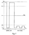
- Figure 1 shows the waveform of normal data together with the waveform of a test signal.
- the normal data extends from a positive voltage VH which is more positive than +5 volts, to a negative voltage VL which is more negative than -5 volts.
- the voltage VH represents logic 0 or the spacing state of the signal and the voltage VL represents logic 1 or the marking state of the signal.
- the test signal extends from VL to VT, where VT is more positive than VL but more negative than -5 volts.
- the range of voltages from -5 volts to +5 volts forms a threshold range between the logic 1 and logic 0 states of the data signal.
- FIG. 1 Also shown in Figure 1 are the positive and negative supply voltages VS+, VS-, which are used to supply the output amplifier of the transmitter.
- VS+ positive and negative supply voltages
- VS- negative supply voltages
- two transistors are connected in series between the supply conductors with the output connection to the line connected to the junction of the two transistors.
- the transistor connected to the negative supply line is rendered conducting whilst the other transistor is non-conducting
- a logic 0 state is to be applied to the line the transistor connected to the positive supply line is rendered conducting whilst that connected to the negative line is non-conducting.
- FIG. 2 is a block diagram of an example of a line interface circuit according to the invention.
- Digital data to be transmitted over a line is applied via a terminal 1 to a transmitter 2.
- the output signal of the transmitter 2 appears on a conductor 3 which is connected through a connector 4 to a conductor 5 of the line.
- Data incoming over the line to the circuit is received along a conductor 6 which is connected by the connector 4 through a conductor 7 to a receiver 8 which produces the incoming data in a required form at a terminal 9.
- the transmitter 2 has additional output conductors 10 and 11 which are connected as inputs to a cross feed unit 12 having an output conductor 13 connected to the receiver 8.
- the cross feed unit 12 is controlled by a loopback mode select signal applied to it via a terminal 14 and a conductor 15A.
- the terminal 14 is connected to a voltage clamp 15 which is connected via a conductor 16 to limit the amplitude of the voltage output from the transmitter 2 when the loopback mode is selected.
- the cross feed unit 12 and the voltage clamp 15 are not operated.
- Digital data from circuits connected to the input of the transmitter 2 and which have the voltages appropriate to those circuits which may be for example, TTL or CMOS, are converted by the transmitter 2 to have the voltage levels VL and VH shown in Figure 1, and are applied via the conductor 3 and the connector 4 to the conductor 5 of the line.
- Data incoming from the line on the conductor 6 have the voltage levels VL and VH and are converted by the receiver 8 to have the voltage levels appropriate to the type of digital circuit connected to the terminal 9.
- an enabling signal is applied to the terminal 14 to select the loopback mode.
- This enabling signal activates the voltage clamp 15 and the cross feed unit 12.
- the effect of the voltage clamp 15 is to restrict the output signal of the transmitter 2 to the voltage levels VL and VT.
- This restriction on the output signal of the transmitter 2 means that any receiver connected to the conductor 5 of the line will interpret the output from the transmitter 2 as a logic 1 because the voltage VT of the test signal is not positive of the -5 volt threshold.
- the logic 1 state output from the transmitter 2 is its rest state.
- the cross feed unit 12 receives via the conductors 10 and 11 the test signal from the transmitter 2 and is enabled by the signal from the terminal 14 to apply that test signal via a conductor 13 to the receiver 8.
- the input circuit of the receiver 8 is so constructed that the effect of the switching between the levels VT and VL when applied by the cross feed unit 12 to the conductor 13 appears to that input circuit to be the same as normal data received along the conductor 6 from the line. In this way the functioning of both the transmitter 2 and the receiver 8 can be tested without the need to disconnect them from the conductors of the line.
- the receiver input circuit is desianed so that, in the loopback mode, any data appearing on the conductor 16 and therefore also on the receiver input 7 is ignored, only data from the cross feed switch 12 being accepted.
- Figure 3 shows in simplified form a circuit of an example of the transmitter 2.
- the conductors 3, 10 and 11 and the terminal 1, shown in Figure 2, are marked in Figure 3.
- the terminal 1 is connected to control a switched current source 20 and also applied to the base of a transistor 21.
- the connections from the terminal 1 to the current source 20 and the base of the transistor 21 may be through an amplifier or other circuit to change the current or voltage ranges as required.
- Both the current source 20 and the emitter of the transistor 21 are connected to a negative supply conductor 22.
- the collector of the transistor 21 is connected to the conductors 3 and 11, and in addition to the collector of a transistor 23.
- the conductors 3 and 11 are connected together; this is not necessarily the case in all forms of the transmitter.
- the emitter of the transistor 23 is connected to the conductor 10 and also through a resistor 24 to a positive supply conductor 25. Two diodes 26 and 27 in series are connected in parallel with the resistor 24.
- the transistor 23 is provided with a second collector which is connected directly to its base to enable the first collector of that transistor to act as a controlled current source.
- the base of the transistor 23 is connected to a contact 28 of a switch SW1 and also to the emitter of a transistor 29.
- the collector of the transistor 29 is connected to the negative supply conductor 22 and its base to a contact 30 of the switch SW1.
- a clamping circuit is connected from the conductors 3 and 11 to the negative supply conductor 22 and consists of diodes 31, 32 and 33 in series with a Darlington transistor 34 the emitter of which is connected to the negative supply conductor 22.
- the base of the Darlington transistor 34 is connected through a current source 35 and a switch SW2 to the positive supply conductor 25.
- the switches SW1 and SW2 are operated together and, as shown in Figure 3, have positions A and B respectively corresponding to the non-selection and the selection of the loopback mode.
- the circuit shown in Figure 3 is constructed as part or all of an integrated circuit with the current sources constructed in a conventional way.
- the switching of the current sources could be effected by providing an alternative path for the current produced by the source when no current is required.
- the switches SW1 and SW2 could be provided by suitably connected transistors controlled by an electrical selection signal.
- the transistor 23 continues to operate as a switch but is limited to supplying a current of about 1 milliamp out of its collector to the conductors 3 and 11 when the current source 20 is supplying current, whereas in normal operation the transistor 23 can supply a much larger current set by the emitter-resistor 24.
- the transistor 21 is switched on and off by the digital signals applied to the terminal 1, but the voltage on its collector is limited in excursion between a voltage close to that of the negative supply conductor 22 when the transistor 21 is conducting, to a voltage, approximately equal to four times the forward conducting voltage of a diode, imposed by the clamping circuit, and in particular by the diodes 31, 32 and 33 and the collector-emitter voltage of the Darlington transistor 34, because in this condition the Darlington transistor 34 is rendered conducting by current from the current source 35.
- the negative supply voltage is -12 volts so that the most positive voltage which is generated on the conductors 3 and 11 is about -9 volts.
- the conductor 10 conveys the voltage at the emitter of the transistor 23 to the cross feed unit 12. If the transistor 23 is operating correctly, then the voltage on the conductor 10 varies between VS+, the voltage on the positive supply conductor 25, and a voltage more negative than VS+ by the forward conducting voltages of the two diodes 26 and 27. If the transistor 23 has failed, then the voltage on the conductor 10 remains at twelve volts because the current supplied by the source 20 is low, and the cross feed unit 12 can be arranged to detect the presence of twelve volts on conductor 10 in these circumstances so as to monitor the operational state of the transistor 23. Failure of the transistor 23 in an open-circuit condition will still allow the voltage on the conductors 3 and 11 to switch between the voltage levels as described above. If, on the other hand, the transistor 23 failed in a short-circuit condition the voltage on conductors 3 and 11 would stay close to the positive supply voltage.
- Figure 4 is a simplified diagram of the cross feed unit 12 shown in Figure 2.
- the conductors 11 form the inputs to a switchable current source 40, the output current of which is fed via a conductor 41 and a resistor 42 to the emitters of transistors 43 and 44.
- the base of the transistor 43 is connected through the diodes 45 and 46 in series to ground and through a resistor 47 to its emitter.
- a collector of the transistor 43 is connected to the conductor 13 to provide the output to the receiver 8.
- the collector of the transistor 44 is connected to a positive supply conductor 48 through a resistor 49.
- the base of the transistor 44 is connected to its emitter through a resistor 50 and to the loopback mode select signal terminal 14 through a resistor 51.
- the base of the transistor 44 is also connected to the base of a transistor 52 having its emitter-collector path connected between the conductor 13 and ground.
- the switchable current source 40 responds to the voltage on the conductor 10 to detect whether or not the transistor 23 ( Figure 3) is functioning or not.
- the voltage on the conductor 11 varies over a range of about three diode forward conduction voltages from about -9 volts to -11.5 volts.
- the current source 40 draws either a zero current or a current of about 60 microamps through the resistor 42.
- a positive voltage supplied to the terminal 14 causes the transistors 44 and 52 to be conducting.
- the transistor 44 serves to bypass the current drawn by the source 40 and the transistor 52 short-circuits the conductor 13 to ground, so that no signals are applied to the receiver.
- both transistors 44 and 52 are non-conducting and the switched currents drawn by the source 40 are drawn from the conductor 13 through the transistor 43. This current drawn from the conductor 13 forms the input to the receiver from the cross feed unit 12.
- Figure 5 shows the input circuit of the receiver R ( Figure 2) with the conductor 13 which connects it to the cross feed unit 12, shown in Figure 4, and the conductor 7 which connects the receiver to the line.
- the conductor 7 is connected through a resistor R which sets the input impedance of the circuit to the value required by the particular standard (in this case EIA-RS232).
- the resistor R is connected to a voltage limiting circuit having diodes 60 and 61 in series connected in parallel with a third diode 62, all in a path to ground.
- the resistor R is also connected through a further resistor 63 to the base of transistor 64 of which the emitter is connected to the conductor 13.
- the collector of the transistor 64 is connected to the remainder of the receiver circuit by a conductor 65 and to a current source 66 joined to a positive supply conductor 67.
- the conductor 65 is connected through diodes 68 and 69 in series to the base of a transistor 70 and also through a resistor 71 to ground.
- the emitter of the transistor 70 is also connected to ground.
- the collector of the transistor 70 is connected through a resistor 72 to the junction of the resistor R and the resistor 63.
- the circuit shown in the rectangle 73 is a simplified equivalent circuit of the cross feed unit shown in Figure 4, showing how a switched current is drawn from the conductor 13 with the pulses of the test signal when the loopback mode is selected.
- the transistor 64 forms the first stage of the receiver and operates as a common emitter amplifier for signals received from the line via conductor 7 and as a common base amplifier for the test signals received as currents via the conductor 13.
- the transistor 70 together with components 68, 69, 71 and 72, serve to provide hysteresis on the input receiver.
- the circuits described above have the following additional advantages.
- the design of the output circuit of the transmitter as shown in Figure 3, together with the use of a clamping circuit to limit the voltage swing on its output during testing, means that it is possible to ensure that in many cases a failure of the output circuit, due to electrical overstress for example, would result in neither the normal data nor the low level test signal being able to be transmitted, so that the satisfactory emission of the test signal would indicate that the circuit would satisfactorily emit the normal data. Faults which interfere with the emission of the normal data but which do not impede the emission of the test signal could occur, and such faults would require other means for their detection.
- the design of the input circuit of the receiver is such that once the correct operation of the transistor 64 has been confirmed, it is possible to say that the receiver is functioning correctly provided that the output signals are obtained as expected.
- the current drawn by the source 40 ( Figure 4) is larger than the current supplied by the source 66 ( Figure 5).
- the loopback mode is not selected, i.e. in the normal mode, the transistor 52 conducts.
- the conductor 65 now sits high or low depending on the state of the receiver input 7 which acts like an inverter. If the input 7 is low, then the conductor 65 is high, and vice versa. In the loopback mode, the transistor 43 conducts.
- the state of the conductor 65 depends wholly on whether the source 40 is on or off. If the source 40 is on, then the condiictor 65 is low, and if the source 40 is off then the conductor 65 is high. It is to be noted that the transistor 44 is used in normal operation to dump the current from the source 40 to the positive supply rail. Transistors 43 and 44 act as a switch. In the loopback mode, the conductor 13 ( Figure 1) is close to zero volts. During operation in the loopback mode the transistor 64 is insensitive to inputs on its base so that any signals incoming to the receiver from the line will be ignored.
Landscapes
- Engineering & Computer Science (AREA)
- Computer Networks & Wireless Communication (AREA)
- Signal Processing (AREA)
- Dc Digital Transmission (AREA)
- Maintenance And Management Of Digital Transmission (AREA)
Claims (16)
- Leitungsschnittstellenschaltung mit:einem Sendermittel (2) mit einem Ausgangsleiter (3) zum Abgeben eines sich zwischen über und unter einem Schwellenwert liegenden stabilen Spannungswerten ändernden Ausgangssignals an eine erste Ader (5) der Leitung;einem Empfängermittel (8) zum Empfangen eines Eingangssignals von einer zweiten Ader (6) der Leitung an einem ersten Eingang; undeinem Mittel (12) zum selektiven direkten Anlegen eines Signals aus dem Sendermittel (2) an das Empfängermittel (8) ohne Durchlaufen der Leitung zum Freigeben der zu testenden Schaltung;dadurch gekennzeichnet, daß das Sendermittel (2) mit Hilfsausgangsleitermitteln (10, 11) zum Abgeben eines Ausgangssignals versehen ist, dessen Amplitude so begrenzt ist, daß es vollständig auf einer Seite des Schwellenwerts liegt;wobei das Mittel (12) zum selektiven Signalanlegen mit den Hilfsausgangsleitermitteln (10, 11) des Sendermittels (2) und mit dem Empfängermittel (8) an dessen zweitem Eingang so verbunden ist, daß es zwischen das Sendermittel (2) und das Empfängermittel (8) eingefügt ist, damit ein Signal aus dem Sendermittel (2) selektiv direkt an das Empfängermittel (8) und unabhängig von der Leitung angelegt wird, um die zu testende Leitungsschnittstellenschaltung freizugeben;wobei ein Mittel (15) mit dem Sendermittel (2) und dem Mittel (12) zum selektiven Signalanlegen verbunden ist, um in selektiver Weise ein einem stabilen Spannungswert des Ausgangssignals entsprechendes Testsignal mit einer solchen Amplitude zu erzeugen, daß das Testsignal daran gehindert ist, den Schwellenwert zu kreuzen;wobei das Empfängermittel (8) ein Mittel enthält, das abhängig von dem Testsignal eine Anzeige des Funktionierens der Leitungsschnittstellenschaltung erzeugt;wobei die Durchführung eines Tests der Leitungsschnittstellenschaltung abhängig von der selektiven Erzeugung eines Testsignals unabhängig von der Verbindung des Ausgangsleiters (3) des Sendermittels (2) mit der ersten Ader (5) der Leitung ist, so daß er unabhängig davon durchführbar ist, ob der Ausgangsleiter (3) des Sendermittels (2) mit der ersten Ader (5) der Leitung verbunden ist.
- Leitungsschnittstellenschaltung nach Anspruch 1, dadurch gekennzeichnet, daß das Hilfsausgangsleitermittel des Sendermittels (2) erste und zweite Hilfsausgangsleiter (10, 11) enthalten, die jeweils über das Mittel (12) zum selektiven Signalanlegen ein Testsignal an das Empfängermittel (8) liefern, das sich zwischen ersten und zweiten stabilen Spannungswerten ändert, von denen jeder daran gehindert ist, den Schwellenwert zu kreuzen.
- Leitungsschnittstellenschaltung nach Anspruch 2, ferner dadurch gekennzeichnet, daß das Mittel zum selektiven Erzeugen eines Testsignals ein mit dem Sendermittel (2) verbundenes Klemmittel (15) enthält, das das Ausgangssignal des Sendermittels (2) während einer Testprozedur auf jeweils an die ersten und zweiten Hilfsausgangsleiter (10, 11) angelegte Spannungswerte und auf eine Amplitude begrenzt, die das Testsignal daran hindert, den Schwellenwert zu kreuzen;daß ein Steuerleiter (15A) vorgesehen ist, der ein an das Klemmittel und an das Mittel (12) zum selektiven Signalanlegen angelegtes Freigabesignal empfängt;wobei das Klemmittel (15) und das Mittel (12) zum selektiven Signalanlegen abhängig vom Auftreten des Freigabesignals an dem Steuerleiter (15A) jeweils betätigt werden;wobei das Klemmittel (15) im betätigten Zustand das von dem Sendermittel (2) an die ersten und zweiten Ausgangsleiter (10, 11) gelieferte Ausgangssignal auf Spannungswerte begrenzt, die das Testsignal daran hindern, den Schwellenwert zu kreuzen; undwobei das Mittel (12) zum selektiven Signalanlegen im betätigten Zustand das Testsignal von den ersten und zweiten Hilfsausgangsleitern (10, 11) des Sendermittels (2) das Testsignal, gehalten auf der Amplitude, erzeugt, die das Testsignal daran hindert, den Schwellenwert zu kreuzen.
- Leitungsschnittstellenschaltung nach Anspruch 3, ferner dadurch gekennzeichnet, daß das Sendermittel (2) enthälterste und zweite Transistoren (21, 23);erste und zweite Spannungsversorgungsleiter (22, 25);wobei die ersten und zweiten Transistoren (21, 23) in Serie zwischen den ersten und zweiten Spannungsversorgungsleitern (22, 25) liegen;einen Verbindungspunkt zwischen den ersten und zweiten Transistoren (21, 23), der an die erste Ader (5) der Leitung angeschlossen ist;wobei die ersten und zweiten Transistoren (21, 23) jeweils bei einem stabilen Spannungswert des Ausgangssignals leitend bzw. nicht leitend und beim anderen stabilen Spannungswert des Ausgangssignals nicht leitend bzw. leitend sind; undwobei der Wert des Ausgangsstroms des ersten Transistors (23) abhängig von der selektiven Erzeugung des Testsignals und der Spannung an dem Verbindungspunkt zwischen den ersten und zweiten Transistoren (21, 23) begrenzt ist, die durch die Wirkung des Klemmittels (31-34) begrenzt ist.
- Leitungsschnittstellenschaltung nach Anspruch 4, ferner gekennzeichnet durch ein Widerstandsmittel (24), das zwischen dem ersten Transistor (23) und dem daran angeschlossenen ersten Spannungsversorgungsleiter (25) liegt; und
wobei der Verbindungspunkt zwischen dem Widerstandsmittel (24) und dem ersten Transistor (23) mit dem Mittel (12) zum selektiven Signalanlegen so verbunden ist, daß dieses Mittel (12) zum selektiven Signalanlegen den Betriebszustand des ersten Transistors (23) überwachen kann. - Leitungsschnittstellenschaltung nach einem der Ansprüche 2 bis 5, ferner dadurch gekennzeichnet, daß das Mittel (12) zum selektiven Signalanlegen (12) eine Querverbindungs-Schaltvorrichtung enthält, die die Testsignale an den ersten und zweiten Hilfsausgangsleitern (10, 11) abwechselnd an den zweiten Eingang des Empfängermittels (8) anlegt.
- Leitungsschnittstellenschaltung nach einem der vorhergehenden Ansprüche, ferner dadurch gekennzeichnet, daß das Empfängermittel (8) außerdem eine erste Stufe enthält, die einen mit einer Steuerkomponente versehenen Transistor (64) aufweist;wobei die Steuerkomponente dieses Transistors (64) des Empfängermittels (8) mit der zweiten Ader (6) der Leitung verbindbar ist; undwobei das Mittel (12) zum selektiven Signalanlegen an eine Elektrodenzone dieses Transistors (64) in der ersten Stufe des Empfängermittels (8) angeschlossen ist.
- Leitungsschnittstellenschaltung nach Anspruch 7, ferner dadurch gekennzeichnet, daß das Mittel (12) zum selektiven Signalanlegen einen geschalteten Strom an die Elektrodenzone des Transistors (64) in der ersten Stufe des Empfängermittels (8) anlegt.
- Leitungsschnittstellenschaltung nach einem der vorhergehenden Ansprüche, dadurch gekennzeichnet, daß an die Leitung angelegte und von dieser Leitung empfangene Ausgangs- und Eingangssignale genormte Signale sind.
- Verfahren zum Testen einer Leitungsschnittstellenschaltung mit einem Sender (2) und einem Empfänger (8) zum Senden und Empfangen eines sich zwischen einem ersten Spannungswert und einem zweiten Spannungswert ändernden Signals zu und von jeweiligen Adern (5, 6) der Leitung, wobei der Sender (2) einen Ausgangssignal an eine erste Ader (5) der Leitung liefert und der Empfänger (8) ein Eingangssignal von einer zweiten Ader (6) der Leitung empfängt, wobei das Verfahren folgende Schritte enthält:Liefern eines Testsignals vom Sender (2) anstelle des Ausgangssignals;Verbinden des Senders (2) mit dem Empfänger (8);selektives Anlegen des Testsignals aus dem Sender (2) an den Empfänger (8); undErfassen des Testsignals, wie es vom Empfänger (8) erzeugt wird;gekennzeichnet durch Erzeugen des Testsignals aus dem Sender (2) anstelle des Ausgangssignals mit einer solchen Amplitudenbegrenzung, daß es vollständig auf einer Seite eines Schwellenwertes liegt, über und unter dem die ersten und zweiten Spannungswerte des Ausgangssignals liegen;direktes Verbinden des Senders (2) mit dem Empfänger (8) unabhängig von den Adern (5, 6) der Leitung;selektives Anlegen des Testsignals aus dem Sender (2) an den Empfänger (8) entsprechend einem stabilen Wert des Ausgangssignals (10, 11) und mit einer Amplitude, die das Testsignal daran hindert, den Schwellenwert zu kreuzen; undErfassen des vom Empfänger (8) erzeugten Testsignals unabhängig von der Verbindung des Senders (10) mit der Ader (5) der Leitung, so daß ein Testen der Leitungsschnittstellenschaltung unabhängig davon erfolgt, ob der Sender (2) an die Ader (5) der Leitung angeschlossen ist.
- Verfahren zum Testen einer Leitungsschnittstellenschaltung nach Anspruch 10, ferner dadurch gekennzeichnet, daß das Testsignal auf der Basis eines der ersten und zweiten Spannungswerte des Ausgangssignals als Signal mit kleiner Amplitude erzeugt wird.
- Verfahren zum Testen einer Leitungsschnittstellenschaltung nach Anspruch 10 oder 11, ferner gekennzeichnet durch abwechselndes Anlegen des Testsignals von ersten und zweiten Hilfsausgangsleitern (10, 11) des Senders (2) als ein sich zwischen ersten und zweiten stabilen Spannungswerten änderndes Testsignal; und
Hindern jedes der ersten und zweiten Spannungswerte, die von den Hilfsausgangsleitern (10, 11) des Senders (2) geliefert werden, am Überkreuzen des Schwellenwertes, wie er zum Empfänger (8) geliefert wird. - Verfahren zum Testen einer Schnittstellenschaltung nach einem der Ansprüche 10 bis 12, ferner gekennzeichnet durch Klemmen des Ausgangssignals des Senders (2) während einer Testprozedur auf Spannungswerte mit einer Amplitude, die das Testsignal daran hindert, den Schwellenwert zu kreuzen.
- Verfahren zum Testen einer Leitungsschnittstellenschaltung nach Anspruch 13, ferner gekennzeichnet durch selektives Anlegen eines Freigabesignals an den Sender (2), damit der Sender in einen Testsignalmodus versetzt wird; und
Erzeugen des Testsignals aus dem Sender (2) für die Eingabe in den Empfänger (8). - Verfahren zum Testen einer Leitungsschnittstellenschaltung nach Anspruch 14, ferner dadurch gekennzeichnet, daß das Klemmen des Ausgangssignals des Senders (2) abhängig von dem Freigabesignal erzielt wird.
- Verfahren zum Testen einer Leitungsschnittstellenschaltung nach einem der Ansprüche 10 bis 15, ferner gekennzeichnet durch Senden eines zusätzlichen Signals aus dem Sender (2) zu dem Empfänger (8), das die Funktionsfähigkeit eines Ausgangstransistors (23) des Senders (2) anzeigt.
Applications Claiming Priority (2)
| Application Number | Priority Date | Filing Date | Title |
|---|---|---|---|
| GB8913952 | 1989-06-16 | ||
| GB898913952A GB8913952D0 (en) | 1989-06-16 | 1989-06-16 | Line interface circuit and method of testing such a circuit |
Publications (3)
| Publication Number | Publication Date |
|---|---|
| EP0403147A2 EP0403147A2 (de) | 1990-12-19 |
| EP0403147A3 EP0403147A3 (de) | 1992-08-26 |
| EP0403147B1 true EP0403147B1 (de) | 1997-01-08 |
Family
ID=10658604
Family Applications (1)
| Application Number | Title | Priority Date | Filing Date |
|---|---|---|---|
| EP90306136A Expired - Lifetime EP0403147B1 (de) | 1989-06-16 | 1990-06-06 | Leistungsschnittstellenschaltung und Verfahren zur Prüfung einer solchen Schaltung |
Country Status (5)
| Country | Link |
|---|---|
| US (1) | US5128962A (de) |
| EP (1) | EP0403147B1 (de) |
| JP (1) | JP3332919B2 (de) |
| DE (1) | DE69029606T2 (de) |
| GB (1) | GB8913952D0 (de) |
Families Citing this family (36)
| Publication number | Priority date | Publication date | Assignee | Title |
|---|---|---|---|---|
| DE4010798A1 (de) * | 1990-04-04 | 1991-10-10 | Bodenseewerk Geraetetech | Demodulatorbaustein und damit aufgebaute signalverarbeitungsschaltung |
| FR2674082B1 (fr) * | 1991-03-14 | 1994-11-25 | Bull Sa | Procedes de test pour transmissions serie bidirectionnelles et circuits pour leur mise en óoeuvre. |
| US5337316A (en) * | 1992-01-31 | 1994-08-09 | Motorola, Inc. | Transceiver self-diagnostic testing apparatus and method |
| SG49316A1 (en) * | 1992-06-26 | 1998-05-18 | Yokogawa Electric Corp | Duplex communication control device |
| WO1994000941A1 (en) * | 1992-06-30 | 1994-01-06 | H. Heuer Instruments Pty. Ltd. | Margin test apparatus for integrated services digital networks |
| GB9306735D0 (en) * | 1993-03-31 | 1993-05-26 | Texas Instruments Ltd | Improvements in or relating to in-circuit testing |
| US5425054A (en) * | 1993-06-23 | 1995-06-13 | Tamarack Microelectronics Inc. | Surrounding circuit for the ethernet coaxial local area newtwork transceiver |
| JP2648796B2 (ja) * | 1993-10-12 | 1997-09-03 | 富士通株式会社 | データ伝送異常検出方式およびデータ伝送機器 |
| AUPM411294A0 (en) * | 1994-02-25 | 1994-03-24 | Martin Communications Pty Ltd | Evaluation of signal processor performance |
| US6255852B1 (en) * | 1999-02-09 | 2001-07-03 | Micron Technology, Inc. | Current mode signal interconnects and CMOS amplifier |
| US7554829B2 (en) | 1999-07-30 | 2009-06-30 | Micron Technology, Inc. | Transmission lines for CMOS integrated circuits |
| US6331785B1 (en) * | 2000-01-26 | 2001-12-18 | Cirrus Logic, Inc. | Polling to determine optimal impedance |
| US6377103B1 (en) | 2000-06-28 | 2002-04-23 | Intel Corporation | Symmetric, voltage-controlled CMOS delay cell with closed-loop replica bias |
| US6348826B1 (en) | 2000-06-28 | 2002-02-19 | Intel Corporation | Digital variable-delay circuit having voltage-mixing interpolator and methods of testing input/output buffers using same |
| US6348811B1 (en) | 2000-06-28 | 2002-02-19 | Intel Corporation | Apparatus and methods for testing simultaneous bi-directional I/O circuits |
| US7222208B1 (en) * | 2000-08-23 | 2007-05-22 | Intel Corporation | Simultaneous bidirectional port with synchronization circuit to synchronize the port with another port |
| US6793575B2 (en) * | 2000-11-10 | 2004-09-21 | Case Venture Management, Llc | Racing game |
| US6795871B2 (en) | 2000-12-22 | 2004-09-21 | General Electric Company | Appliance sensor and man machine interface bus |
| US6720801B2 (en) * | 2001-06-18 | 2004-04-13 | The United States Of America As Represented By The Secretary Of The Navy | RS-232 bus data tap apparatus |
| US6791356B2 (en) * | 2001-06-28 | 2004-09-14 | Intel Corporation | Bidirectional port with clock channel used for synchronization |
| US7180352B2 (en) * | 2001-06-28 | 2007-02-20 | Intel Corporation | Clock recovery using clock phase interpolator |
| US6950968B1 (en) * | 2001-07-31 | 2005-09-27 | Alcatel | System and method for conducting diagnostics in a telecommunications node |
| US7101770B2 (en) * | 2002-01-30 | 2006-09-05 | Micron Technology, Inc. | Capacitive techniques to reduce noise in high speed interconnections |
| US6900116B2 (en) | 2002-03-13 | 2005-05-31 | Micron Technology Inc. | High permeability thin films and patterned thin films to reduce noise in high speed interconnections |
| US7235457B2 (en) * | 2002-03-13 | 2007-06-26 | Micron Technology, Inc. | High permeability layered films to reduce noise in high speed interconnects |
| US6846738B2 (en) * | 2002-03-13 | 2005-01-25 | Micron Technology, Inc. | High permeability composite films to reduce noise in high speed interconnects |
| US7192892B2 (en) | 2003-03-04 | 2007-03-20 | Micron Technology, Inc. | Atomic layer deposited dielectric layers |
| US6970053B2 (en) * | 2003-05-22 | 2005-11-29 | Micron Technology, Inc. | Atomic layer deposition (ALD) high permeability layered magnetic films to reduce noise in high speed interconnection |
| US9529762B2 (en) * | 2003-06-30 | 2016-12-27 | Becton, Dickinson And Company | Self powered serial-to-serial or USB-to-serial cable with loopback and isolation |
| US7366641B1 (en) | 2005-03-28 | 2008-04-29 | Western Digital Technologies, Inc. | Serial interface amplitude selection for a disk drive in an unknown interconnect environment |
| US7927948B2 (en) | 2005-07-20 | 2011-04-19 | Micron Technology, Inc. | Devices with nanocrystals and methods of formation |
| US20070104111A1 (en) * | 2005-11-04 | 2007-05-10 | Intel Corporation | Internal analog loopback for a high-speed interface test |
| US7280302B1 (en) | 2005-11-16 | 2007-10-09 | Western Digital Technologies, Inc. | Disk drive using loopback to calibrate transmission amplitude |
| US20080195920A1 (en) * | 2007-02-13 | 2008-08-14 | Freescale Semiconductor, Inc. | Self-test structure and method of testing a digital interface |
| KR101369834B1 (ko) * | 2007-07-25 | 2014-03-05 | 삼성전자주식회사 | 시리얼 데이터 수신장치 및 이를 사용한 전자장치 |
| CN102055339B (zh) * | 2009-10-30 | 2014-03-26 | 深圳富泰宏精密工业有限公司 | 测试用电源装置 |
Family Cites Families (3)
| Publication number | Priority date | Publication date | Assignee | Title |
|---|---|---|---|---|
| FR2485306A1 (fr) * | 1980-06-23 | 1981-12-24 | Trt Telecom Radio Electr | Systeme de test local d'un modem utilisant la modulation par deplacement de frequence |
| DE3472874D1 (en) * | 1984-08-24 | 1988-08-25 | Ibm | Line interface |
| US4993045A (en) * | 1988-10-31 | 1991-02-12 | Racal Data Communications Inc. | Modem diagnostic loop |
-
1989
- 1989-06-16 GB GB898913952A patent/GB8913952D0/en active Pending
-
1990
- 1990-05-15 US US07/523,784 patent/US5128962A/en not_active Expired - Fee Related
- 1990-06-06 EP EP90306136A patent/EP0403147B1/de not_active Expired - Lifetime
- 1990-06-06 DE DE69029606T patent/DE69029606T2/de not_active Expired - Fee Related
- 1990-06-16 JP JP15854190A patent/JP3332919B2/ja not_active Expired - Fee Related
Non-Patent Citations (1)
| Title |
|---|
| PATENT ABSTRACTS OF JAPAN vol. 013, no. 374 (E-808)18 August 1989 &JP-A-11 026 841 * |
Also Published As
| Publication number | Publication date |
|---|---|
| DE69029606T2 (de) | 1997-04-24 |
| DE69029606D1 (de) | 1997-02-20 |
| GB8913952D0 (en) | 1989-08-02 |
| EP0403147A2 (de) | 1990-12-19 |
| JPH03129949A (ja) | 1991-06-03 |
| EP0403147A3 (de) | 1992-08-26 |
| JP3332919B2 (ja) | 2002-10-07 |
| US5128962A (en) | 1992-07-07 |
Similar Documents
| Publication | Publication Date | Title |
|---|---|---|
| EP0403147B1 (de) | Leistungsschnittstellenschaltung und Verfahren zur Prüfung einer solchen Schaltung | |
| US5488306A (en) | Open and short fault detector for a differential interface | |
| US4220876A (en) | Bus terminating and decoupling circuit | |
| US4385394A (en) | Universal interface for data communication systems | |
| US4490673A (en) | Testing an integrated circuit containing a tristate driver and a control signal generating network therefor | |
| US3541441A (en) | Test system for evaluating amplitude and response characteristics of logic circuits | |
| US6873272B2 (en) | Integrated analog-to-digital converter with detection of external faults | |
| US3941950A (en) | Telephone line testing instrument having a supervising capability | |
| US4984250A (en) | DC termination circuit for subscriber cables | |
| EP0266519A1 (de) | Schaltung zum Nachweis von unterbrochenen Leitern | |
| US4656643A (en) | Line interface circuit | |
| US6445239B1 (en) | Bus coupling with amplitude-controlled transmission circuit | |
| US4685113A (en) | Driver isolating circuit for common bus-type transmission of local area network | |
| US4879661A (en) | Bi-directional circuit to interface between a low current device and high current tester | |
| AU708184B2 (en) | Probe for fault actuation devices | |
| US3983324A (en) | Full duplex driver/receiver | |
| US4788458A (en) | Two wire interface circuit | |
| US6696851B2 (en) | Reception line break detection apparatus | |
| GB2064918A (en) | Data communication systems | |
| EP0618696B1 (de) | In-circuit-Testen von Komponenten | |
| US4201979A (en) | Conveying data signals between relatively rotatable units | |
| US3194988A (en) | Hub driver utilizing clamping network and means to controllably isolate hub circuit from clamping network | |
| JPH0799820B2 (ja) | 回線切替装置 | |
| JPH04108243A (ja) | インタフェース自動切換回路 | |
| JPH0548425A (ja) | 論理回路の送り終端方式の伝送試験方法 |
Legal Events
| Date | Code | Title | Description |
|---|---|---|---|
| PUAI | Public reference made under article 153(3) epc to a published international application that has entered the european phase |
Free format text: ORIGINAL CODE: 0009012 |
|
| AK | Designated contracting states |
Kind code of ref document: A2 Designated state(s): DE FR GB IT NL |
|
| RIN1 | Information on inventor provided before grant (corrected) |
Inventor name: FATTORI, FRANK R. Inventor name: KERSLAKE, RICHARD M. |
|
| PUAL | Search report despatched |
Free format text: ORIGINAL CODE: 0009013 |
|
| AK | Designated contracting states |
Kind code of ref document: A3 Designated state(s): DE FR GB IT NL |
|
| 17P | Request for examination filed |
Effective date: 19921102 |
|
| 17Q | First examination report despatched |
Effective date: 19941123 |
|
| GRAG | Despatch of communication of intention to grant |
Free format text: ORIGINAL CODE: EPIDOS AGRA |
|
| GRAH | Despatch of communication of intention to grant a patent |
Free format text: ORIGINAL CODE: EPIDOS IGRA |
|
| GRAH | Despatch of communication of intention to grant a patent |
Free format text: ORIGINAL CODE: EPIDOS IGRA |
|
| GRAA | (expected) grant |
Free format text: ORIGINAL CODE: 0009210 |
|
| AK | Designated contracting states |
Kind code of ref document: B1 Designated state(s): DE FR GB IT NL |
|
| PG25 | Lapsed in a contracting state [announced via postgrant information from national office to epo] |
Ref country code: NL Free format text: LAPSE BECAUSE OF FAILURE TO SUBMIT A TRANSLATION OF THE DESCRIPTION OR TO PAY THE FEE WITHIN THE PRESCRIBED TIME-LIMIT Effective date: 19970108 |
|
| ITF | It: translation for a ep patent filed | ||
| REF | Corresponds to: |
Ref document number: 69029606 Country of ref document: DE Date of ref document: 19970220 |
|
| ET | Fr: translation filed | ||
| NLV1 | Nl: lapsed or annulled due to failure to fulfill the requirements of art. 29p and 29m of the patents act | ||
| PLBE | No opposition filed within time limit |
Free format text: ORIGINAL CODE: 0009261 |
|
| STAA | Information on the status of an ep patent application or granted ep patent |
Free format text: STATUS: NO OPPOSITION FILED WITHIN TIME LIMIT |
|
| 26N | No opposition filed | ||
| PGFP | Annual fee paid to national office [announced via postgrant information from national office to epo] |
Ref country code: GB Payment date: 20010502 Year of fee payment: 12 |
|
| PGFP | Annual fee paid to national office [announced via postgrant information from national office to epo] |
Ref country code: FR Payment date: 20010531 Year of fee payment: 12 |
|
| PGFP | Annual fee paid to national office [announced via postgrant information from national office to epo] |
Ref country code: DE Payment date: 20010627 Year of fee payment: 12 |
|
| REG | Reference to a national code |
Ref country code: GB Ref legal event code: IF02 |
|
| PG25 | Lapsed in a contracting state [announced via postgrant information from national office to epo] |
Ref country code: GB Free format text: LAPSE BECAUSE OF NON-PAYMENT OF DUE FEES Effective date: 20020606 |
|
| PG25 | Lapsed in a contracting state [announced via postgrant information from national office to epo] |
Ref country code: DE Free format text: LAPSE BECAUSE OF NON-PAYMENT OF DUE FEES Effective date: 20030101 |
|
| GBPC | Gb: european patent ceased through non-payment of renewal fee |
Effective date: 20020606 |
|
| PG25 | Lapsed in a contracting state [announced via postgrant information from national office to epo] |
Ref country code: FR Free format text: LAPSE BECAUSE OF NON-PAYMENT OF DUE FEES Effective date: 20030228 |
|
| REG | Reference to a national code |
Ref country code: FR Ref legal event code: ST |
|
| PG25 | Lapsed in a contracting state [announced via postgrant information from national office to epo] |
Ref country code: IT Free format text: LAPSE BECAUSE OF NON-PAYMENT OF DUE FEES;WARNING: LAPSES OF ITALIAN PATENTS WITH EFFECTIVE DATE BEFORE 2007 MAY HAVE OCCURRED AT ANY TIME BEFORE 2007. THE CORRECT EFFECTIVE DATE MAY BE DIFFERENT FROM THE ONE RECORDED. Effective date: 20050606 |