EP0402533A1 - Residuenarithmetisches Gerät - Google Patents
Residuenarithmetisches Gerät Download PDFInfo
- Publication number
- EP0402533A1 EP0402533A1 EP19890201507 EP89201507A EP0402533A1 EP 0402533 A1 EP0402533 A1 EP 0402533A1 EP 19890201507 EP19890201507 EP 19890201507 EP 89201507 A EP89201507 A EP 89201507A EP 0402533 A1 EP0402533 A1 EP 0402533A1
- Authority
- EP
- European Patent Office
- Prior art keywords
- output
- modulo
- residue
- inputs
- representation
- Prior art date
- Legal status (The legal status is an assumption and is not a legal conclusion. Google has not performed a legal analysis and makes no representation as to the accuracy of the status listed.)
- Granted
Links
Images


Classifications
-
- G—PHYSICS
- G06—COMPUTING OR CALCULATING; COUNTING
- G06F—ELECTRIC DIGITAL DATA PROCESSING
- G06F7/00—Methods or arrangements for processing data by operating upon the order or content of the data handled
- G06F7/60—Methods or arrangements for performing computations using a digital non-denominational number representation, i.e. number representation without radix; Computing devices using combinations of denominational and non-denominational quantity representations, e.g. using difunction pulse trains, STEELE computers, phase computers
- G06F7/72—Methods or arrangements for performing computations using a digital non-denominational number representation, i.e. number representation without radix; Computing devices using combinations of denominational and non-denominational quantity representations, e.g. using difunction pulse trains, STEELE computers, phase computers using residue arithmetic
- G06F7/729—Methods or arrangements for performing computations using a digital non-denominational number representation, i.e. number representation without radix; Computing devices using combinations of denominational and non-denominational quantity representations, e.g. using difunction pulse trains, STEELE computers, phase computers using residue arithmetic using representation by a residue number system
-
- G—PHYSICS
- G06—COMPUTING OR CALCULATING; COUNTING
- G06F—ELECTRIC DIGITAL DATA PROCESSING
- G06F7/00—Methods or arrangements for processing data by operating upon the order or content of the data handled
- G06F7/60—Methods or arrangements for performing computations using a digital non-denominational number representation, i.e. number representation without radix; Computing devices using combinations of denominational and non-denominational quantity representations, e.g. using difunction pulse trains, STEELE computers, phase computers
- G06F7/72—Methods or arrangements for performing computations using a digital non-denominational number representation, i.e. number representation without radix; Computing devices using combinations of denominational and non-denominational quantity representations, e.g. using difunction pulse trains, STEELE computers, phase computers using residue arithmetic
- G06F7/722—Modular multiplication
Definitions
- the basic input operands may be initially converted to their "logarithms" according to the following table.
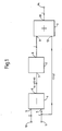
- the output 8 of the look-up table 2 is connected to the input 9 of the adder 3 a second input 12 of which is connected to the input terminal 11 and is hence fed with the representation of the input quantity y .
- the output 13 of adder 3 is connected to the apparatus output 14.
- Subtractor 1 generates a representation of the quantity (x-y) at its output 6.
- the Zech table is the following Input (x-y) g x-y g x-y +1 Output j Nil 0 1 0 0 1 2 1 1 2 3 4 2 4 5 9 3 8 9 8 4 3 4 2 5 6 7 11 6 12 0 Nil 7 11 12 6 8 9 10 10 9 5 6 5 10 10 11 7 11 7 8 3
- the entries "Nil” indicate the special state that corresponds to a number zero, which cannot be represented in the form g n and has to be represented differently.
- n n mod 3 n mod 4 0 0 0 1 1 1 2 2 2 3 0 3 4 1 0 5 2 1 6 0 2 7 1 3 8 2 0 9 0 1 10 1 2 11 2 3
- the representations used for the input and output quantities of the adder and subtractor subcircuits may of course be chosen at will. They may, for example each be in the form of a one-out-of- m code, where m is the corresponding said respective integer; such a choice can give a considerable degree of protection against incorrect results being obtained due, for example, to the presence of noise.
- the part of the block diagram of Figure 2 which is shown in full lines comprises, similarly to the known apparatus shown in Figure 1, a subtractor 1, a look-up table 2 and an adder 3, connected as shown.
- subtractor 1 now comprises two subtractor subcircuits 1A and 1B respectively and adder 3 now comprises two adder subcircuits 3A and 3B respectively.
- the apparatus input 10 now has two components 10A and 10B which constitute respective non-overlapping fields thereof and the apparatus input 11 now has two components 11A and 11B which constitute respective non-overlapping fields thereof.
- the components 10A and 11A are connected to respective inputs 4A and 5A of the subtractor subcircuit 1A and the components 10B and 11B are connected to respective inputs 4B and 5B of the subtractor subcircuit 1B.
- the input 7 of the look-up table 2 now has two components 7A and 7B which constitute respective non-overlapping fields thereof and to which are connected the outputs 6A and 6B of the subtractor respectively.
- the outputs 6A and 6B constitute respective non-overlapping fields of the subtractor output 6.
- the output 8 of the look-up table 2 similarly now has two components 8A and 8B which constitute respective non-overlapping fields thereof and which are connected to first inputs 9A and 9B of the adder subcircuits 3A and 3B respectively.
- the components 11A and 11B of the apparatus input 11 are connected to second inputs 12A and 12B of the adder subcircuits 3A and 3B respectively.
- the apparatus output 14 now has two components 14A and 14B which constitute respective non-overlapping fields thereof and to which are connected the outputs 13A and 13B of the adder subcircuits 3A and 3B respectively.
- the outputs 13A and 13B constitute respective non-overlapping fields of the adder circuit output 13.
- the further components shown in dashed lines will be referred to below.
- the subtractor subcircuit 1A is arranged to generate at its output 6A a residue representation modulo a specific integer n 1 of the difference (x1-y2) between first and second quantities x1 and y1 in response to the application of residue representations of these quantities modulo n 1 to its inputs 4A and 5A respectively.
- the subtractor subcircuit 1B is arranged to generate at its output 6B a residue representation modulo a specific integer n 2 of the difference (x2-y2) between first and second quantities x1 and x2 in response to the application of residue representations of these quantities modulo n 2 to its inputs 4B and 5B respectively.
- n 1 and n 2 are mutually prime, i.e. they have no factors other than unity in common.
- the subtractor 1 consisting of the subtractor subcircuits 1A and 1B therefore responds to the application of representations of quantities x and y to the apparatus inputs 10 and 11 respectively, each of these representations being in residue form modulo n 1 and n 2, i.e. x being in the form x1 mod n 1, x2 mod n 2 and y being in the form y1 mod n1, y2 mod n 2 where the representations of x1, x2, y1 and y2 are applied to the fields 10A, 10B, 11A and 11B respectively of the apparatus inputs 10 and 11, by generating at its output 6 a representation of x-y.
- residue representations are applied as residue components k1 and k2 respectively to the fields 7A and 7B respectively of the input 7 of the look-up table 2.
- the adder subcircuit 3A is arranged to generate at its output 13A a residue representation modulo n 1 of the sum (r1+j1) of first and second quantities r1 and j1 in response to the application of residue representations of these quantities modulo n 1 to its inputs 12A and 9A respectively.
- the adder subcircuit 3B is arranged to generate at its output 13A a residue representation modulo n2 of the sum (r2+j2) of first and second quantities r2 and j2 in response to the application of residue representations of these quantities modulo n 2 to its inputs 12B and 9B respectively.
- i is the power index to which the generator g has to be raised to give the value (X+Y), as required.
- the residue representations may each be, for example, in the form of a compact binary code or a "one out of m" code, wherein m is the modulus used for the relevant representation.
- the inputs 10A and 10B of Figure 2 may be n1 bits wide and n2 bits wide respectively, as may be the inputs 11A and 11B and the outputs 14A and 14B, each possible value of the relevant representation then being denoted by a value of binary "1" (or"0") for a respective one of the relevant bits.
- n1 and n2 are 3 and 4 respectively then the numbers n from 0 to 11 can, for example, be represented as follows: n n mod 3 n mod 4 0 001 0001 1 010 0010 2 100 0100 3 001 1000 4 010 0001 5 100 0010 6 001 0100 7 010 1000 8 100 0001 9 001 0010 10 010 0100 11 100 1000
- the entries "Nil” may be represented by a particular unique code, for example 111 0000.
- Such a relationship can be obtained, for example, by suitably programming a read-only memory the address input of which is fed with the input code.
- it can be obtained by means of a suitably configured combinatorial logic circuit.
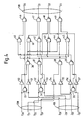
- Figure 3 is the circuit diagram of a possible construction for the modulo 3 adder subcircuit 3A of Figure 2 if the coding specified above, and the particular code specified for "Nil", are employed.
- the particular construction shown is suitable for implentation by means of a programmed logic array (PLA) and comprises twelve NAND gates 15-26 and six inverters 27-32 interconnected and connected to the inputs 12A and 9A, and the output 13A, as shown.
- the successive bits y10, y11, Y12 (reading from right to left above) of the code for quantity y1 are applied to respective lines of the input 12A as shown, and the successive bits j10, j11, j12 of the code for the quantity j1 are applied to respective lines of the input 9A as shown.
- the successive bits i10, i11, i12 of the code for the quantity i1 appear on respective lines of the output 13A as shown. Inspection will reveal that the truth table for the construction of Figure 3 is that required.
- the circuit configuration of Figure 3 is also suitable for use as the modulo 3 subtractor subcircuit 1A of Figure 2, in which case the references 12A, 9A, 13A, y10, y11, y12, j10, j11, j12, i10, i11 and i12 used at the inputs and output should be replaced by 4A, 5A, 6A, x10, x11, x12, y10, y12, y11, (x1-y1)0, (x1-y1)1 and (x1-y1)2 respectively, where x10, x11 and x12 are the successive bits of the code for the quantity x1 and (x1-y1) o , (x1-y1)1 and (x1-y1)2 are the successive bits of the code for the quantity (x1-y1). (These replacements make use of the fact that, in modulo (p-1) arithmetic, the negative of a number is equal to (p-1) minus that number).
- Figure 4 is the circuit diagram of a possible construction for the modulo 4 adder subcircuit 3B of Figure 2 if the specified coding is employed.
- This construction is also suitable for implementation by means of a programmed logic array and comprises seventeen NAND gates 33-49 and eight inverters 50-57 interconnected and connected to the inputs 12B and 9B, and the output 13B, as shown.
- the successive bits y20, y21, y22 and y23 of the code for the quantity y2 are applied to respective lines of the input 12B as shown, and the successive bits j20, j21, j22 and j23 of the code for the quantity j2 are applied to respective lines of the input 9B as shown.
- the successive bits i20, i21, i22 and i23 of the code for the quantity i2 appear on respective lines of the output 13B as shown.
- the circuit configuration of Figure 4 is also suitable for use as the modulo 4 subtractor subcircuit 1B of Figure 2, in which case the references 12B, 9B, 13B, y20, y21, y22, y23, j20, j21, j22, j23, i20, i21, i22, and i23 used at the inputs and output should be replaced by 4B, 5B, 6B, x20, x21, x22.
- the further components shown in dashed lines in Figure 2 may also be provided, these being a decoder 58 having inputs 59 and 60 connected to the components 11A and 11B respectively of the apparatus input 11, and a multiplexer 61 the control input 62 of which is conected to the output 63 of decoder 58.
- Components 64A and 64B of a first signal input 64 of multiplexer 61 are connected to the components 10A and 10B of the apparatus input 10 and components 65A and 65B of a second signal input 65 of the multiplexer 61 are connected to the outputs 13A and 13B respectively of the adder circuit 3.
- Components 14A′ and 14B′ of the output 14′ of multiplexer 61 constitute respective components of the new output of the apparatus.
- Decoder 58 is constructed to detect the code for "nil" on the apparatus input 11A, 11B and produce a signal on its output 63 when this occurs.
- Multiplexer 61 is constructed to respond to the presence of such a signal on its control input 62 by connecting the components 64A and 64B of its first input 64 to the components 14A′ and 14B′ respectively of its output 14, the components 65A and 65B of its second input 65 being connected to the components 14A′ and 14B′ respectively otherwise. The result is therefore that the apparatus produces the same output codes at its output 14A′, 14B′ as it does at its output 14A, 14B except when the code applied to the input 11A, 11B is "nil". When this last is the case the code x1, x2 appears at the output 14A′, 14B′, as required.
- the look-up table circuit 2 of Figure 2 may alternatively be arranged to generate at its output 8A, 8B a residue representation modulo (p-1) of the power index j to which g has to be raised to give the value g k -1 in modulo p arithmetic in response to the application to its input 7A, 7B of a representation modulo (p-1) of any member of a set of values of k .
- the plural residue representation generated at the output 14A, 14B will be of the power index i to which g has to be raised to give the value (X-Y) in modulo p arithmetic, instead of (X+Y).
- the values of n1 and n2 are 3 and 4 respectively as used above in the illustrative example discussed with reference to Figure 2, and the input and output quantities of the look-up table 2 are again each represented as a one-out-of-three code together with a one-out-of-four code as discussed previously, then in the alternative the look-up table 2 may be programmed to give the following relationship between its input and output codes.
- Input code Output code Nil 001 0100 001 0001 Nil 010 0010 001 0001 100 0100 010 0001 001 1000 100 1000 010 0001 010 0010 100 0010 001 0010 001 0100 010 1000 010 1000 010 0100 100 0001 001 1000 001 0010 100 0100 010 0100 100 0001 100 1000 100 0010
- subtractor circuit 1 will have to comprise three subtractor subcircuits which operate modulo 4, modulo 5 and modulo 9 respectively and which are fed from respective corresponding non-overlapping fields of the inputs 10 and 11, and adder circuit 3 will similarly have to comprise three adder subcircuits which operate modulo 4, modulo 5 and modulo 9 respectively and which are fed from respective corresponding non-overlapping fields of the input 11 and the output 8 of look-up table 2.
- the look-up table 2 of Figure 2 may be formed, for example, by a suitably programmed read-only memory, a respective non-overlapping field of each output word thereof constituting the output 8A and the output 8B.
- a suitably programmed read-only memory may alternatively be employed for this purpose, respective fields of the address input of each one of these being fed from the outputs 6A and 6B of subtractor subcircuits 1A and 1B respectively and the outputs of these memories constituting the outputs 8A and 8B respectively.
- the look-up table 2 of Figure 2 may, as another example, be formed by means of combinatorial logic.
- each combination of codes applied to the inputs 7A and 7B may be manipulated by logic circuitry to produce a binary "1" (or "0") on a respective one out of, in the example, thirteen lines, thereby indicating the presence of a respective one of the thirteen possible input states.
- This binary "1” or “0” can then be used to drive a further logic circuit which, in response, generates the required corresponding codes on the outputs 8A and 8B.
- the same coding scheme is used for the quantities represented throughout the apparatus, it will be evident that this is not necessarily the case.
- a one-out-of-N coding scheme may be used for the quantities x1, x2, y1, y2, i1 and i2 whereas the subtractor circuits 1A and 1B and the look-up table 2 may be constructed to produce their outputs in the form of a conventional compact binary code, the look-up table 2 and the adder subcircuits 3A and 3B being modified accordingly so as to respond in the desired manner to the compact binary codes used.
Landscapes
- Physics & Mathematics (AREA)
- General Physics & Mathematics (AREA)
- Engineering & Computer Science (AREA)
- Computational Mathematics (AREA)
- Mathematical Analysis (AREA)
- Mathematical Optimization (AREA)
- Pure & Applied Mathematics (AREA)
- Theoretical Computer Science (AREA)
- Computing Systems (AREA)
- Mathematical Physics (AREA)
- General Engineering & Computer Science (AREA)
- Error Detection And Correction (AREA)
Priority Applications (1)
| Application Number | Priority Date | Filing Date | Title |
|---|---|---|---|
| DE1989627673 DE68927673T2 (de) | 1989-06-12 | 1989-06-12 | Residuenarithmetisches Gerät |
Applications Claiming Priority (1)
| Application Number | Priority Date | Filing Date | Title |
|---|---|---|---|
| GB8810167A GB2217883B (en) | 1988-04-29 | 1988-04-29 | Arithmetic apparatus |
Publications (2)
| Publication Number | Publication Date |
|---|---|
| EP0402533A1 true EP0402533A1 (de) | 1990-12-19 |
| EP0402533B1 EP0402533B1 (de) | 1997-01-15 |
Family
ID=10636093
Family Applications (1)
| Application Number | Title | Priority Date | Filing Date |
|---|---|---|---|
| EP89201507A Expired - Lifetime EP0402533B1 (de) | 1988-04-29 | 1989-06-12 | Residuenarithmetisches Gerät |
Country Status (3)
| Country | Link |
|---|---|
| US (1) | US5008849A (de) |
| EP (1) | EP0402533B1 (de) |
| GB (1) | GB2217883B (de) |
Families Citing this family (7)
| Publication number | Priority date | Publication date | Assignee | Title |
|---|---|---|---|---|
| US5623423A (en) * | 1994-12-12 | 1997-04-22 | Univ. Of Texas | Apparatus and method for video decoding |
| US5944774A (en) * | 1997-09-26 | 1999-08-31 | Ericsson Inc. | Methods apparatus and computer program products for accumulating logarithmic values |
| US6226271B1 (en) | 1997-09-26 | 2001-05-01 | Ericsson Inc. | Received signal strength determination method, apparatus and computer program products |
| JP4279626B2 (ja) * | 2003-07-31 | 2009-06-17 | 株式会社アドバンテスト | 剰余系演算システム、スケーリング演算器、スケーリング演算方法、及びそのプログラムと記録媒体 |
| US8060550B2 (en) * | 2005-09-27 | 2011-11-15 | Southern Methodist University | Method and apparatus for integer transformation using a discrete logarithm and modular factorization |
| US7739323B2 (en) * | 2006-06-20 | 2010-06-15 | International Business Machines Corporation | Systems, methods and computer program products for providing a combined moduli-9 and 3 residue generator |
| US7849125B2 (en) | 2006-07-07 | 2010-12-07 | Via Telecom Co., Ltd | Efficient computation of the modulo operation based on divisor (2n-1) |
Family Cites Families (1)
| Publication number | Priority date | Publication date | Assignee | Title |
|---|---|---|---|---|
| US4742479A (en) * | 1985-03-25 | 1988-05-03 | Motorola, Inc. | Modulo arithmetic unit having arbitrary offset and modulo values |
-
1988
- 1988-04-29 GB GB8810167A patent/GB2217883B/en not_active Expired - Lifetime
-
1989
- 1989-05-01 US US07/345,391 patent/US5008849A/en not_active Expired - Fee Related
- 1989-06-12 EP EP89201507A patent/EP0402533B1/de not_active Expired - Lifetime
Non-Patent Citations (2)
| Title |
|---|
| IEEE TRANSACTIONS ON COMPUTERS, vol. C-25, no. 11, November 1976, pages 1057-1067; YAU et al.: "On the design of modulo arithmetic units based on cyclic groups" * |
| MacWILLIAMS et al.: "The theory of error-correcting codes", Part I, chapter 3, 1977, pages 90-92, North-Holland Publishing Co., Amsterdam, NL * |
Also Published As
| Publication number | Publication date |
|---|---|
| GB2217883A (en) | 1989-11-01 |
| US5008849A (en) | 1991-04-16 |
| GB8810167D0 (en) | 1988-06-02 |
| EP0402533B1 (de) | 1997-01-15 |
| GB2217883B (en) | 1992-06-10 |
Similar Documents
| Publication | Publication Date | Title |
|---|---|---|
| US4168530A (en) | Multiplication circuit using column compression | |
| EP0239899B1 (de) | Matrix-strukturierte Multiplizierschaltung | |
| JP3244506B2 (ja) | 小型乗算器 | |
| Elleithy et al. | Fast and flexible architectures for RNS arithmetic decoding | |
| EP0158530B1 (de) | Dividierer ohne Rückstellung | |
| US3670956A (en) | Digital binary multiplier employing sum of cross products technique | |
| JPH0157814B2 (de) | ||
| JPS6375932A (ja) | ディジタル乗算器 | |
| Taylor | Compatible hardware for division and square root | |
| JPS60164837A (ja) | 除算装置 | |
| US4366549A (en) | Multiplier with index transforms modulo a prime or modulo a fermat prime and the fermat prime less one | |
| EP0402533B1 (de) | Residuenarithmetisches Gerät | |
| JPH0713741A (ja) | アルファ合成演算器 | |
| US3842250A (en) | Circuit for implementing rounding in add/subtract logic networks | |
| Ercegovac et al. | Very high radix division with selection by rounding and prescaling | |
| US5365471A (en) | Divider for performing signed division using a redundant signed digit | |
| EP0402532A1 (de) | Residuenarithmetisches Gerät | |
| EP0643352A1 (de) | Selbstprüfender komplementärer Addierer | |
| US3287546A (en) | Parity prediction apparatus for use with a binary adder | |
| US4974188A (en) | Address sequence generation by means of reverse carry addition | |
| US20050246406A9 (en) | Emod a fast modulus calculation for computer systems | |
| GB2226165A (en) | Parallel carry generation adder | |
| GB2130774A (en) | Circuits for operating on N-digit operands | |
| JPH076024A (ja) | 十進数乗算器 | |
| CN116149605A (zh) | 模数乘法电路与计算模数乘法的方法 |
Legal Events
| Date | Code | Title | Description |
|---|---|---|---|
| PUAI | Public reference made under article 153(3) epc to a published international application that has entered the european phase |
Free format text: ORIGINAL CODE: 0009012 |
|
| AK | Designated contracting states |
Kind code of ref document: A1 Designated state(s): DE FR GB |
|
| 17P | Request for examination filed |
Effective date: 19910613 |
|
| RAP3 | Party data changed (applicant data changed or rights of an application transferred) |
Owner name: N.V. PHILIPS' GLOEILAMPENFABRIEKEN Owner name: PHILIPS ELECTRONICS UK LIMITED |
|
| 17Q | First examination report despatched |
Effective date: 19931209 |
|
| GRAG | Despatch of communication of intention to grant |
Free format text: ORIGINAL CODE: EPIDOS AGRA |
|
| GRAH | Despatch of communication of intention to grant a patent |
Free format text: ORIGINAL CODE: EPIDOS IGRA |
|
| GRAH | Despatch of communication of intention to grant a patent |
Free format text: ORIGINAL CODE: EPIDOS IGRA |
|
| GRAA | (expected) grant |
Free format text: ORIGINAL CODE: 0009210 |
|
| AK | Designated contracting states |
Kind code of ref document: B1 Designated state(s): DE FR GB |
|
| REF | Corresponds to: |
Ref document number: 68927673 Country of ref document: DE Date of ref document: 19970227 |
|
| ET | Fr: translation filed | ||
| PGFP | Annual fee paid to national office [announced via postgrant information from national office to epo] |
Ref country code: GB Payment date: 19970602 Year of fee payment: 9 |
|
| PGFP | Annual fee paid to national office [announced via postgrant information from national office to epo] |
Ref country code: FR Payment date: 19970624 Year of fee payment: 9 |
|
| PGFP | Annual fee paid to national office [announced via postgrant information from national office to epo] |
Ref country code: DE Payment date: 19970822 Year of fee payment: 9 |
|
| PLBE | No opposition filed within time limit |
Free format text: ORIGINAL CODE: 0009261 |
|
| STAA | Information on the status of an ep patent application or granted ep patent |
Free format text: STATUS: NO OPPOSITION FILED WITHIN TIME LIMIT |
|
| 26N | No opposition filed | ||
| PG25 | Lapsed in a contracting state [announced via postgrant information from national office to epo] |
Ref country code: GB Free format text: LAPSE BECAUSE OF NON-PAYMENT OF DUE FEES Effective date: 19980612 |
|
| GBPC | Gb: european patent ceased through non-payment of renewal fee |
Effective date: 19980612 |
|
| PG25 | Lapsed in a contracting state [announced via postgrant information from national office to epo] |
Ref country code: FR Free format text: LAPSE BECAUSE OF NON-PAYMENT OF DUE FEES Effective date: 19990226 |
|
| PG25 | Lapsed in a contracting state [announced via postgrant information from national office to epo] |
Ref country code: DE Free format text: LAPSE BECAUSE OF NON-PAYMENT OF DUE FEES Effective date: 19990401 |
|
| REG | Reference to a national code |
Ref country code: FR Ref legal event code: ST |