EP0401577A1 - Metal oxide-semiconductor device and fabrication method of the same - Google Patents
Metal oxide-semiconductor device and fabrication method of the same Download PDFInfo
- Publication number
- EP0401577A1 EP0401577A1 EP90109511A EP90109511A EP0401577A1 EP 0401577 A1 EP0401577 A1 EP 0401577A1 EP 90109511 A EP90109511 A EP 90109511A EP 90109511 A EP90109511 A EP 90109511A EP 0401577 A1 EP0401577 A1 EP 0401577A1
- Authority
- EP
- European Patent Office
- Prior art keywords
- region
- single crystal
- insulator
- semiconductor substrate
- crystal semiconductor
- Prior art date
- Legal status (The legal status is an assumption and is not a legal conclusion. Google has not performed a legal analysis and makes no representation as to the accuracy of the status listed.)
- Granted
Links
- 239000004065 semiconductor Substances 0.000 title claims abstract description 65
- 238000000034 method Methods 0.000 title claims description 36
- 238000004519 manufacturing process Methods 0.000 title description 4
- 239000002184 metal Substances 0.000 title 1
- 239000000758 substrate Substances 0.000 claims abstract description 70
- 239000012212 insulator Substances 0.000 claims abstract description 58
- 239000012535 impurity Substances 0.000 claims abstract description 41
- 239000013078 crystal Substances 0.000 claims abstract description 39
- 230000000694 effects Effects 0.000 claims abstract description 22
- 230000008030 elimination Effects 0.000 claims abstract description 15
- 238000003379 elimination reaction Methods 0.000 claims abstract description 15
- 238000005468 ion implantation Methods 0.000 claims description 14
- 230000003647 oxidation Effects 0.000 claims description 11
- 238000007254 oxidation reaction Methods 0.000 claims description 11
- 229910021421 monocrystalline silicon Inorganic materials 0.000 claims description 7
- 238000005530 etching Methods 0.000 claims description 5
- 238000000137 annealing Methods 0.000 claims description 4
- 238000000926 separation method Methods 0.000 claims description 3
- 238000000151 deposition Methods 0.000 claims description 2
- 238000009792 diffusion process Methods 0.000 claims description 2
- 230000004913 activation Effects 0.000 claims 1
- 230000001590 oxidative effect Effects 0.000 claims 1
- 238000000059 patterning Methods 0.000 claims 1
- VYPSYNLAJGMNEJ-UHFFFAOYSA-N Silicium dioxide Chemical compound O=[Si]=O VYPSYNLAJGMNEJ-UHFFFAOYSA-N 0.000 description 28
- 229910052814 silicon oxide Inorganic materials 0.000 description 28
- XUIMIQQOPSSXEZ-UHFFFAOYSA-N Silicon Chemical compound [Si] XUIMIQQOPSSXEZ-UHFFFAOYSA-N 0.000 description 19
- 229910052710 silicon Inorganic materials 0.000 description 19
- 239000010703 silicon Substances 0.000 description 19
- 230000015556 catabolic process Effects 0.000 description 12
- 229910021420 polycrystalline silicon Inorganic materials 0.000 description 12
- 229920005591 polysilicon Polymers 0.000 description 12
- 229910052796 boron Inorganic materials 0.000 description 10
- -1 oxygen ions Chemical class 0.000 description 8
- 230000003071 parasitic effect Effects 0.000 description 7
- 229920002120 photoresistant polymer Polymers 0.000 description 6
- 230000001133 acceleration Effects 0.000 description 5
- 238000002955 isolation Methods 0.000 description 5
- ZOXJGFHDIHLPTG-UHFFFAOYSA-N Boron Chemical compound [B] ZOXJGFHDIHLPTG-UHFFFAOYSA-N 0.000 description 4
- 230000015572 biosynthetic process Effects 0.000 description 4
- 235000012431 wafers Nutrition 0.000 description 4
- 230000003247 decreasing effect Effects 0.000 description 3
- VEXZGXHMUGYJMC-UHFFFAOYSA-N Hydrochloric acid Chemical compound Cl VEXZGXHMUGYJMC-UHFFFAOYSA-N 0.000 description 2
- 229910052785 arsenic Inorganic materials 0.000 description 2
- RQNWIZPPADIBDY-UHFFFAOYSA-N arsenic atom Chemical compound [As] RQNWIZPPADIBDY-UHFFFAOYSA-N 0.000 description 2
- 238000010586 diagram Methods 0.000 description 2
- 238000009413 insulation Methods 0.000 description 2
- 150000002500 ions Chemical class 0.000 description 2
- 230000007935 neutral effect Effects 0.000 description 2
- 229910052698 phosphorus Inorganic materials 0.000 description 2
- 239000011574 phosphorus Substances 0.000 description 2
- 238000001020 plasma etching Methods 0.000 description 2
- 229910021332 silicide Inorganic materials 0.000 description 2
- FVBUAEGBCNSCDD-UHFFFAOYSA-N silicide(4-) Chemical compound [Si-4] FVBUAEGBCNSCDD-UHFFFAOYSA-N 0.000 description 2
- OAICVXFJPJFONN-UHFFFAOYSA-N Phosphorus Chemical compound [P] OAICVXFJPJFONN-UHFFFAOYSA-N 0.000 description 1
- 239000000969 carrier Substances 0.000 description 1
- 230000005465 channeling Effects 0.000 description 1
- 238000010276 construction Methods 0.000 description 1
- 238000011109 contamination Methods 0.000 description 1
- 230000008021 deposition Effects 0.000 description 1
- 238000010438 heat treatment Methods 0.000 description 1
- 230000010354 integration Effects 0.000 description 1
- 238000003475 lamination Methods 0.000 description 1
- 238000012986 modification Methods 0.000 description 1
- 230000004048 modification Effects 0.000 description 1
- 229910052760 oxygen Inorganic materials 0.000 description 1
- 239000001301 oxygen Substances 0.000 description 1
Images


Classifications
-
- H—ELECTRICITY
- H01—ELECTRIC ELEMENTS
- H01L—SEMICONDUCTOR DEVICES NOT COVERED BY CLASS H10
- H01L29/00—Semiconductor devices adapted for rectifying, amplifying, oscillating or switching, or capacitors or resistors with at least one potential-jump barrier or surface barrier, e.g. PN junction depletion layer or carrier concentration layer; Details of semiconductor bodies or of electrodes thereof ; Multistep manufacturing processes therefor
- H01L29/66—Types of semiconductor device ; Multistep manufacturing processes therefor
- H01L29/66007—Multistep manufacturing processes
- H01L29/66075—Multistep manufacturing processes of devices having semiconductor bodies comprising group 14 or group 13/15 materials
- H01L29/66227—Multistep manufacturing processes of devices having semiconductor bodies comprising group 14 or group 13/15 materials the devices being controllable only by the electric current supplied or the electric potential applied, to an electrode which does not carry the current to be rectified, amplified or switched, e.g. three-terminal devices
- H01L29/66409—Unipolar field-effect transistors
- H01L29/66477—Unipolar field-effect transistors with an insulated gate, i.e. MISFET
- H01L29/66742—Thin film unipolar transistors
- H01L29/66772—Monocristalline silicon transistors on insulating substrates, e.g. quartz substrates
-
- H—ELECTRICITY
- H01—ELECTRIC ELEMENTS
- H01L—SEMICONDUCTOR DEVICES NOT COVERED BY CLASS H10
- H01L29/00—Semiconductor devices adapted for rectifying, amplifying, oscillating or switching, or capacitors or resistors with at least one potential-jump barrier or surface barrier, e.g. PN junction depletion layer or carrier concentration layer; Details of semiconductor bodies or of electrodes thereof ; Multistep manufacturing processes therefor
- H01L29/66—Types of semiconductor device ; Multistep manufacturing processes therefor
- H01L29/68—Types of semiconductor device ; Multistep manufacturing processes therefor controllable by only the electric current supplied, or only the electric potential applied, to an electrode which does not carry the current to be rectified, amplified or switched
- H01L29/76—Unipolar devices, e.g. field effect transistors
- H01L29/772—Field effect transistors
- H01L29/78—Field effect transistors with field effect produced by an insulated gate
-
- H—ELECTRICITY
- H01—ELECTRIC ELEMENTS
- H01L—SEMICONDUCTOR DEVICES NOT COVERED BY CLASS H10
- H01L21/00—Processes or apparatus adapted for the manufacture or treatment of semiconductor or solid state devices or of parts thereof
- H01L21/02—Manufacture or treatment of semiconductor devices or of parts thereof
- H01L21/04—Manufacture or treatment of semiconductor devices or of parts thereof the devices having at least one potential-jump barrier or surface barrier, e.g. PN junction, depletion layer or carrier concentration layer
- H01L21/18—Manufacture or treatment of semiconductor devices or of parts thereof the devices having at least one potential-jump barrier or surface barrier, e.g. PN junction, depletion layer or carrier concentration layer the devices having semiconductor bodies comprising elements of Group IV of the Periodic System or AIIIBV compounds with or without impurities, e.g. doping materials
-
- H—ELECTRICITY
- H01—ELECTRIC ELEMENTS
- H01L—SEMICONDUCTOR DEVICES NOT COVERED BY CLASS H10
- H01L29/00—Semiconductor devices adapted for rectifying, amplifying, oscillating or switching, or capacitors or resistors with at least one potential-jump barrier or surface barrier, e.g. PN junction depletion layer or carrier concentration layer; Details of semiconductor bodies or of electrodes thereof ; Multistep manufacturing processes therefor
- H01L29/66—Types of semiconductor device ; Multistep manufacturing processes therefor
- H01L29/68—Types of semiconductor device ; Multistep manufacturing processes therefor controllable by only the electric current supplied, or only the electric potential applied, to an electrode which does not carry the current to be rectified, amplified or switched
- H01L29/76—Unipolar devices, e.g. field effect transistors
- H01L29/772—Field effect transistors
- H01L29/78—Field effect transistors with field effect produced by an insulated gate
- H01L29/786—Thin film transistors, i.e. transistors with a channel being at least partly a thin film
- H01L29/78606—Thin film transistors, i.e. transistors with a channel being at least partly a thin film with supplementary region or layer in the thin film or in the insulated bulk substrate supporting it for controlling or increasing the safety of the device
- H01L29/78609—Thin film transistors, i.e. transistors with a channel being at least partly a thin film with supplementary region or layer in the thin film or in the insulated bulk substrate supporting it for controlling or increasing the safety of the device for preventing leakage current
-
- H—ELECTRICITY
- H01—ELECTRIC ELEMENTS
- H01L—SEMICONDUCTOR DEVICES NOT COVERED BY CLASS H10
- H01L29/00—Semiconductor devices adapted for rectifying, amplifying, oscillating or switching, or capacitors or resistors with at least one potential-jump barrier or surface barrier, e.g. PN junction depletion layer or carrier concentration layer; Details of semiconductor bodies or of electrodes thereof ; Multistep manufacturing processes therefor
- H01L29/66—Types of semiconductor device ; Multistep manufacturing processes therefor
- H01L29/68—Types of semiconductor device ; Multistep manufacturing processes therefor controllable by only the electric current supplied, or only the electric potential applied, to an electrode which does not carry the current to be rectified, amplified or switched
- H01L29/76—Unipolar devices, e.g. field effect transistors
- H01L29/772—Field effect transistors
- H01L29/78—Field effect transistors with field effect produced by an insulated gate
- H01L29/786—Thin film transistors, i.e. transistors with a channel being at least partly a thin film
- H01L29/78651—Silicon transistors
- H01L29/78654—Monocrystalline silicon transistors
Definitions
- the MOS integrated circuits are required to have a breakdown voltage which is about two times as large as the supply voltage in consideration of the noise in the supply voltage and the substrate biasing.
- the breakdown voltage is usually set to 5 volts, the breakdown voltage of 10 volts or less is apparently insufficient.
- this prior art MOS transistor can eliminate the back channel effect by the isolated doped region interrupting the formation of the inversion layer extending between the source and drain regions along the boundary to the underlying silicon oxide substrate, it has a problem in that a neutral region is formed in the channel region because of the relatively large thickness of the channel layer (about 0.5 ⁇ m) which prevents the depletion region formed during the operation of the transistor from extending to and reaching the boundary to the underlying silicon oxide layer. When this occurs, there is a possibility that holes, which may be formed during the operation of the transistor as a result of impact ionization, are accumulated in the neutral region.
- the silicon single crystal layer is biased with respect to the source region and there appears a parasitic bipolar action in the parasitic bipolar transistor formed by the source region, drain region and the channel region intervening therebwtween.
- a parasitic bipolar action occurs, a large amount of carriers are caused to flow between the source and drain regions and the breakdown voltage between the source and drain regions is significantly decreased.
- the MOS transistor of this reference is also disadvantageous from the viewpoint of forming a parasitic capacitance under the overhanging drain region which reduces the operational speed of the transistor.
- such a MOS transistor having the offset gate structure occupies a large area and is disadvantageous from the view point of increasing the integration density of the integrated circuit.
- the resistance caused by the overhanging drain region provides an effect of reducing the operational speed.
- an SOI semiconductor body including a silicon oxide substrate 10 and a p-type single crystal silicon layer 11 is subjected to a thermal oxidation process wherein a silicon oxide film 12 having a thickness of about 200 ⁇ is formed on the silicon layer 11.
- the single crystal silicon layer 11 are divided into a number of portions which are separated from each other by a silicon oxide isolation region 19.
- the SOI semiconductor body may be formed by binding a pair of semiconductor wafers each having an oxidized surface such that the oxidized surfaces are contacted each other.
- the SOI semiconductor body may be formed by the so-called SIMOX process wherein oxygen ions are selectively implanted to a semiconductor wafer in correspondence to the depth of the silicon substrate.
- the p-type silicon layer 11 has a thickness of about 0.1 ⁇ m and a specific resistance of about 10 ⁇ .cm.
- the SOI semiconductor body is used in a state that it is supported by a silicon wafer.
- the silicon oxide film 12 is formed on the p-type silicon layer 11 in order to prevent the contamination of the silicon layer 11 from the photoresist applied in the subsequent process and at the same time for preventing the occurrence of the channeling in response to the ion implantation. Further, the silicon oxide film 12 acts to remove the impurities from the silicon layer 11 and protects the surface of the silicon layer 11.
- a photoresist 13 is applied on the top surface of the silicon oxide film 12 and a part thereof having a size D is removed photolithographically as a window in correspondence to the gate electrode to be formed in the later process.
- the size D is chosen to be 0.5 ⁇ m as will be described.
- an ion implantation of boron (B+) is performed under an acceleration voltage of 30 - 40 keV with a dose of 3 X 1013 cm ⁇ 2.
- the boron ions are implanted into the silicon layer 11 in correspondence to the removed part of the photoresist.
- Most of the boron ions thus implanted reach the depth close to the boundary between the silicon layer 11 and the silicon oxide layer 10 underneath as shown in FIG.4C.
- the photoresist 13 is removed and the silicon oxide film 12 is removed also subsequently.
- the substrate thus obtained is subjected to a thermal oxidation under hydrochloride vapor at a temperature between 900 - 950°C.
- a gate insulation film 15 is formed on the surface of the silicon layer 11.
- the implanted boron ions are activated and a p+-type region 16 of increased impurity concentration level is formed as illustrated in FIG.4D.
- the dotted boundary of the region 16 shows the concentration profile of boron which is reduced by a factor of about two orders of magnitude (102) with respect to the maximum concentration of boron in the region 16.
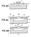
- a gate electrode 17 of polysilicon is deposited on the gate insulator film 15 by a CVD process and patterned subsequently such that the gate electrode 17 remains above the region 16 for a gate length L of 0.8 ⁇ m as shown in FIG.4E.
- This gate electrode 17 may be a lamination of polysilicon and silicide.
- the alignment between the patterned gate electrode 17 and the region 16 located below the gate electrode 17 can be achieved with an alignment accuracy within about 0.03 ⁇ m using the same stepper.
- the size D of the window formed in the photoresist 13 is chosen such that the size D is smaller than the gate length L by 0.2 - 0.3 ⁇ m or more. As already described, the size D is set to 0.5 ⁇ m and the gate length L is set to 0.8 ⁇ m in the foregoing embodiment. By choosing the size D of the window as such, the region 16 remains invariably smaller than the gate electrode 17.
- a silicon oxide film 22 is deposited on the layer 21 by a low temperature CVD process at a temperature of 400°C for a thickness of 200 ⁇ , and a part of the polysilicon layer 21 and the silicon oxide film 22 corresponding to the gate of the MOS transistor to be formed is removed by etching for a size L′ to form an window 100.
- This size L′ corresponds to the gate length of the desired MOS transistor.
- FIG.5D shows the semiconductor device after the foregoing processes.
- the region 25 for eliminating the back channel effect is separated from the source and drain regions 26.
- the p+-type region 25 does not form the p-n junction with the source or drain region 26 directly, and thereby the problem of unwanted decrease of the drain breakdown voltage is successfully eliminated.
Abstract
Description
- The present invention generally relates to metal-oxide-semiconductor (MOS) devices and more particularly to a MOS device having the semiconductor-on-insulator (SOI) structure wherein the back channel effect is eliminated.
- In conventional MOS transistors, the increase of operational speed of the device is limited because of the parasitic capacitance formed between the source/drain region and the substrate. In a MOS transistor having the SOI structure wherein a thin semiconductor layer acting as the substrate is provided on an insulator layer, such a parasitic capacitance is decreased significantly and a high speed operation can be achieved. Such a device also has a preferable feature of near-ideal isolation between the semiconductor devices and associated therewith, the device generally has a high breakdown voltage.
- FIG.1 shows a typical structure of the MOS transistor formed on an SOI substrate. Referring to the drawing, the SOI substrate includes a
silicon wafer 40 and asilicon oxide layer 41 provided thereon. On thesilicon oxide layer 41, there is formed a usual MOS transistor having a single crystalsilicon substrate layer 42, source anddrain regions 46 formed in thelayer 42, achannel region 44 intervening between the source anddrain regions 46, and agate electrode 45 provided on thelayer 42. Thesubstrate layer 42 is isolated from the substrate layer of adjacent transistors by anisolation region 43 of silicon oxide. In the drawing, illustration of the gate insulation film is omitted. - Although such a structure is effective in reducing the parasitic capacitance, there arises a problem that a so-called back channel effect is tend to be caused. In the back channel effect, electric charges are accumulated at the interface between
silicon substrate layer 42 and thesilicon oxide layer 41 underneath, and such electric charges provide a back channel extending across the source and drain regions along the interface. In response to the appearance of the back channel effect, a leak current flows across the source and drain regions as illustrated by the arrow in FIG.1. - As the back channel is an conductive inversion layer formed by the electric charges in the
insulator layer 41, and the formation of the back channel can be reduced when the impurity concentration is increased. In other words, the back channel effect can be suppressed by increasing the impurity concentration of thesemiconductor layer 42 acting as the substrate of the MOS transistor. For example, Japanese Laid-open Patent Application No.58-64064 discloses a MOS transistor having the SOI structure wherein the semiconductor layer providing the channel region between the source and the drain regions is doped by ion implantation of impurities such that the concentration level of the impurities therein changes with three distinct concentration levels with the depth of the semiconductor layer. In this prior art, the concentration level adjacent to the insulator layer is maximized for eliminating the back channel effect. - Alternately, there is disclosed a similar technique for eliminating the back channel effect in the Japanese Laid-open Patent Application 60-220425. FIG.2 shows the general feature of the MOS transistor disclosed in these prior art references. In such a MOS transistor, the
channel region 44 is divided into the normal channel region 44a having a normal impurity concentration level and a back channeleffect eliminating region 47 doped to an increased impurity concentration level. Thisregion 47 is formed adjacent to thesilicon oxide layer 41. Similarly to FIG.1, theregion 46 represents the source and drain regions and theregion 45 represents the gate electrode. - In the MOS transistor of FIG.2, the back channel effect is successfully eliminated as a result of the provision of the
region 47. However, such a structure has a problem of poor breakdown characteristic because of the reason that theregion 47 which is doped for example to the p-type with the high concentration level is located in contact with the source ordrain region 46 which is doped to the n-type with the high concentration level. More specifically, such a device shows a decrease of the breakdown voltage to less than 10 volts when theregion 47 is doped to the level of 2 X 10¹⁷ cm⁻³ In the usual device wherein theregion 47 is not provided and thechannel region 44 is doped in the level of 1 X 10¹⁶ cm⁻³, on the other hand, the breakdown voltage is usually about 50 volts. - Generally, the MOS integrated circuits are required to have a breakdown voltage which is about two times as large as the supply voltage in consideration of the noise in the supply voltage and the substrate biasing. As the supply voltage is usually set to 5 volts, the breakdown voltage of 10 volts or less is apparently insufficient.
- Further, there is a known MOS transistor disclosed in the Japanese Laid-open Patent Application No.62-104172 having an offset gate structure. The MOS transistor is constructed on a silicon single crystal layer provided on a silicon oxide substrate and has an isolated doped region having an increased impurity concentration level in the channel region formed in the silicon single crystal layer in correspondence to a boundary between the silicon oxide substrate and the silicon single crystal layer for eliminating the back channel effect. This isolated doped region is provided under an overhanging drain region characterizing the offset gate structure but is separated therefrom and further in an offset relationship with respect to the gate electrode provided on the silicon single crystal layer. Although this prior art MOS transistor can eliminate the back channel effect by the isolated doped region interrupting the formation of the inversion layer extending between the source and drain regions along the boundary to the underlying silicon oxide substrate, it has a problem in that a neutral region is formed in the channel region because of the relatively large thickness of the channel layer (about 0.5 µm) which prevents the depletion region formed during the operation of the transistor from extending to and reaching the boundary to the underlying silicon oxide layer. When this occurs, there is a possibility that holes, which may be formed during the operation of the transistor as a result of impact ionization, are accumulated in the neutral region. In response thereto, the silicon single crystal layer is biased with respect to the source region and there appears a parasitic bipolar action in the parasitic bipolar transistor formed by the source region, drain region and the channel region intervening therebwtween. When such a parasitic bipolar action occurs, a large amount of carriers are caused to flow between the source and drain regions and the breakdown voltage between the source and drain regions is significantly decreased. The MOS transistor of this reference is also disadvantageous from the viewpoint of forming a parasitic capacitance under the overhanging drain region which reduces the operational speed of the transistor. Further, such a MOS transistor having the offset gate structure occupies a large area and is disadvantageous from the view point of increasing the integration density of the integrated circuit. Furthermore, the resistance caused by the overhanging drain region provides an effect of reducing the operational speed.
- Accordingly, it is a general object of the present invention to provide a novel and useful MOS transistor and a fabrication method thereof, wherein the foregoing problems are eliminated.
- Another object of the present invention is to provide a metal-oxide-semiconductor device having a semiconductor-on-insulator structure, comprising: an insulator substrate; a single crystal semiconductor substrate provided on the insulator substrate, the single crystal semiconductor substrate and the insulator substrate forming a part of the semiconductor-on-insulator structure;
source and drain regions doped to a first conduction type and defined in the single crystal semiconductor substrate; a channel region defined in the single crystal semiconductor substrate so as to be interposed between the source and drain regions, the channel region being doped to a second conduction type opposite to the first conduction type with a first impurity concentration level; a gate insulator film provided on the single crystal semiconductor substrate in correspondence to the channel region; and a gate electrode provided on the gate insulator film in correspondence to the channel region with a predetermined gate length; wherein the channel region is defined by a back channel elimination region having an increased impurity concentration level exceeding the first impurity concentration level such that the back channel elimination region is located adjacent to the insulator substrate for eliminating the back channel effect taking place therethrough, the back channel elimination region being provided under the gate electrode in a manner such that the back channel elimination region is separated from the source and the drain regions by a region having an impurity concentration level smaller than the increased impurity concentration level. According to the present invention, the back channel effect is successfully eliminated by the use of the region of increased impurity concentration while maintaining a satisfactory break down voltage as a result of forming the region so as to be separated from the source and drain regions of the MOS transistor. - Other objects and further features of the present invention will become apparent from the following detailed description when read in conjunction with attached drawings.
-
- FIG.1 is a cross-sectional view showing a prior art MOS transistor having an SOI structure;
- FIG.2 is a cross-sectional view showing another prior art MOS transistor having a structure for eliminating the back channel effect;
- FIG.3 is a cross-sectional view showing a first embodiment of the present invention;
- FIGS.4A - 4E are diagrams showing various steps of fabricating the MOS transistor of FIG.3; and
- FIGS.5A - 5E are diagrams showing another process of fabricating a MOS transistor having the SOI structure wherein the back channel effect is eliminated.
- Hereinafter, a first embodiment of the MOS transistor according to the present invention will be described together with the fabrication steps thereof with reference to FIG.3 and FIGS.4A - 4E.
- Referring to FIG.4A at first, an SOI semiconductor body including a
silicon oxide substrate 10 and a p-type single crystal silicon layer 11 is subjected to a thermal oxidation process wherein asilicon oxide film 12 having a thickness of about 200 Å is formed on the silicon layer 11. It should be noted that the single crystal silicon layer 11 are divided into a number of portions which are separated from each other by a siliconoxide isolation region 19. The SOI semiconductor body may be formed by binding a pair of semiconductor wafers each having an oxidized surface such that the oxidized surfaces are contacted each other. Alternatively, the SOI semiconductor body may be formed by the so-called SIMOX process wherein oxygen ions are selectively implanted to a semiconductor wafer in correspondence to the depth of the silicon substrate. In any case, the p-type silicon layer 11 has a thickness of about 0.1 µm and a specific resistance of about 10 Ω.cm. In order to maintain a sufficient mechanical strength, it is usual that the SOI semiconductor body is used in a state that it is supported by a silicon wafer. - The
silicon oxide film 12 is formed on the p-type silicon layer 11 in order to prevent the contamination of the silicon layer 11 from the photoresist applied in the subsequent process and at the same time for preventing the occurrence of the channeling in response to the ion implantation. Further, thesilicon oxide film 12 acts to remove the impurities from the silicon layer 11 and protects the surface of the silicon layer 11. - Next, in a step of FIG.4B, a
photoresist 13 is applied on the top surface of thesilicon oxide film 12 and a part thereof having a size D is removed photolithographically as a window in correspondence to the gate electrode to be formed in the later process. The size D is chosen to be 0.5 µm as will be described. - Next, using the photoresist thus patterned as the mask, an ion implantation of boron (B⁺) is performed under an acceleration voltage of 30 - 40 keV with a dose of 3 X 10¹³ cm⁻². Upon the ion implantation, the boron ions are implanted into the silicon layer 11 in correspondence to the removed part of the photoresist. Most of the boron ions thus implanted reach the depth close to the boundary between the silicon layer 11 and the
silicon oxide layer 10 underneath as shown in FIG.4C. - Next, the
photoresist 13 is removed and thesilicon oxide film 12 is removed also subsequently. Next, the substrate thus obtained is subjected to a thermal oxidation under hydrochloride vapor at a temperature between 900 - 950°C. Thereby, agate insulation film 15 is formed on the surface of the silicon layer 11. At the same time to the process of oxidation, the implanted boron ions are activated and a p⁺-type region 16 of increased impurity concentration level is formed as illustrated in FIG.4D. In FIG.4D, the dotted boundary of theregion 16 shows the concentration profile of boron which is reduced by a factor of about two orders of magnitude (10²) with respect to the maximum concentration of boron in theregion 16. - Next, a
gate electrode 17 of polysilicon is deposited on thegate insulator film 15 by a CVD process and patterned subsequently such that thegate electrode 17 remains above theregion 16 for a gate length L of 0.8 µm as shown in FIG.4E. Thisgate electrode 17 may be a lamination of polysilicon and silicide. The alignment between thepatterned gate electrode 17 and theregion 16 located below thegate electrode 17 can be achieved with an alignment accuracy within about 0.03 µm using the same stepper. - Next, using the
gate electrode 17 as the mask, ion implantation of arsenic (As⁺) is made under an acceleration voltage of 60 keV for a dose of 5 X 10¹⁵cm⁻², and after a subsequent annealing, source and drainregions 18 are formed in the semiconductor layer 11. Further, by removing thesilicon oxide film 15 from a region covering the source and drainregions 18, a MOS transistor shown in FIG.3 is completed wherein the source and drainregions 18 as well as achannel region 4 intervening therebetween are provided in the substrate 11 which in turn is provided on theinsulator layer 10. As can be seen, the gate electrode extends between the source and drainregions 18 in a manner to cover a part of the source and drainregions 18 while theregion 16 is provided immediately under thegate electrode 17 with a separation from the source and drainregions 18. This transistor is isolated from adjacent transistors by theisolation region 19 of silicon oxide which is formed already at the beginning of the process of FIG.4A. - In the foregoing process, the size D of the window formed in the
photoresist 13 is chosen such that the size D is smaller than the gate length L by 0.2 - 0.3 µm or more. As already described, the size D is set to 0.5 µm and the gate length L is set to 0.8 µm in the foregoing embodiment. By choosing the size D of the window as such, theregion 16 remains invariably smaller than thegate electrode 17. - According to the foregoing construction, the formation of unwanted p-n junction between the
region 16 and the source or drainregion 18, which otherwise would cause the decrease of the breakdown voltage, is eliminated because of theregion 16 having a size smaller than the separation between the source and drainregions 18. Even when the diffusion of implanted boron ions may occur as a result of the accompanying annealing such that the tail of the compositional profile defining theregion 16 is contacted with the source or drainregion 18, the concentration of boron in such a contacting region can be held small and does not cause any substantial decrease of the breakdown voltage. Thus, the present invention can successfully eliminate the back channel effect while without causing the decrease of the breakdown voltage. - Next, a second embodiment of the present invention will be described with reference to FIGS.5A - 5E. In the drawings, the parts corresponding to the parts already described with reference to preceding drawings are given identical reference numerals and the description thereof will be omitted.
- Referring to FIG.5A at first, a
polysilicon layer 21 is deposited on the silicon layer II including theisolation region 19 for a thickness of 2000 - 3000 Å by a CVD process. Next, thepolysilicon layer 21 is doped with phosphorus (P) with a concentration determined such that thelayer 21 has a surface resistivity of about 20 Ω/□. Thislayer 21 is used later as the source and drain regions of the MOS transistor. Thislayer 21 may be formed as a laminated structure of polysilicon and silicide. The doping may be made by ion implantation under an acceleration voltage of 50 keV, and a does of 5 X 10¹⁵cm⁻² is used when phosphorus ions are doped. In the case of doping thepolysilicon layer 21 by arsenic, the acceleration voltage is changed to 60 keV. - Next, a
silicon oxide film 22 is deposited on thelayer 21 by a low temperature CVD process at a temperature of 400°C for a thickness of 200 Å, and a part of thepolysilicon layer 21 and thesilicon oxide film 22 corresponding to the gate of the MOS transistor to be formed is removed by etching for a size L′ to form anwindow 100. This size L′ corresponds to the gate length of the desired MOS transistor. - Further, a
silicon oxide layer 23 shown in FIG.5A by a broken line is deposited on the structure by a low temperature CVD process for 2000 Å and thelayer 23 is subsequently subjected to anisotropic etching process proceeding vertically to the surface of thelayer 22 until the top surface of the substrate 11 is exposed in correspondence to the window L′. This anisotropic etching process may be performed by the reactive ion etching (RIE) process. Thereby, theoxide layer 23 is remained at the side wall of thewindow 100 substantially unetched, and there is formed awindow 100′ having a reduced size D′ as shown in FIG.5B. By the foregoing process, the size D′ of thewindow 100′ is smaller than the size L′ of thewindow 100 by 0.3 - 0.4 µm. - Next, the structure of FIG.5B is subjected to ion implantation of B⁺ under an acceleration voltage of 30 - 40 keV with a dose of 3 X 10¹³ X cm⁻². In this ion implantation, the
polysilicon layer 23 remaining at the side wall of thewindow 100′ acts as the mask and the ion implantation is made only in correspondence to thewindow 100′ having the size D′ as shown in FIG.5C. It should be noted that the implanted boron ions reach a depth corresponding to the boundary between the single crystal silicon layer 11 and theinsulator layer 10 underneath as illustrated therein. BF₂ may also be used as the ions to be implanted. - Next, a
silicon oxide film 23 remaining in the structure of FIG.5C is removed completely, and a newsilicon oxide film 24 is formed as shown in FIG.5D by thermal oxidation at 900 - 950°C under the existence of hydrochloride. Thissilicon oxide film 24 has a thickness of 200 Å for example and acts as the gate insulator film. It should be noted that during this thermal oxidation process, the oxidation proceeds more rapidly in the surface of thepolysilicon layer 21 than in the surface of the single crystal silicon layer 11. Thus, the thickness of thesilicon oxide layer 24 has a thickness of 400 - 500 Å at the side wall of the window which now has an increased size as illustrated by areference numeral 100˝ as well as on the top surface of thelayer 21, and because of this, a sufficient breakdown voltage is secured between the gate electrode and the polysilicon layer. - At the time of the heat treatment associated with the formation of the
gate insulator film 24, the implanted boron ions are activated, and a p⁺region 25 is formed. This p⁺region 25 corresponds to theregion 16 of the MOS transistor of the first embodiment, and acts as a layer for eliminating the back channel effect. The dotted boundary of theregion 25 represents the concentration profile of B⁺ which is decreased by a factor of 10² similarly to the case of theregion 16. Further, P⁺ ions incorporated into thepolysilicon layer 21 by the ion implantation are diffused into the single crystal silicon layer 11 at the time of foregoing thermal oxidation, and thereby source and drainregions 26 of the n⁺-type are formed in the layer 11. FIG.5D shows the semiconductor device after the foregoing processes. - Next, a
gate electrode 27 is provided in correspondence to thewindow 100˝. It should be noted that thewindow 100˝ has the size which is substantially identical to the size L′ of thewindow 100, as thewindow 100˝ is smaller than thewindow 100 only by the thickness of thesilicon oxide layer 24 which is, as already described, only about 400 - 500 Å. Thus, the MOS transistor thus formed has the gate length which is substantially identical to the size L′. After the deposition of thegate electrode 27, thesilicon oxide layer 24 covering thepolysilicon layer 21 is removed and the fabrication of the MOS transistor is completed. - It should be noted that, in this transistor, too, the
region 25 for eliminating the back channel effect is separated from the source and drainregions 26. In other words, the p⁺-type region 25 does not form the p-n junction with the source or drainregion 26 directly, and thereby the problem of unwanted decrease of the drain breakdown voltage is successfully eliminated. - Further, the present invention is not limited to these embodiments described heretofore but various variations and modifications may be made without departing from the scope of the invention.
Claims (11)
characterized in that the channel region is defined with a back channel elimination region (16, 25) having an increased impurity concentration level exceeding the first impurity concentration level such that the back channel elimination region is located adjacent to the insulator substrate for eliminating the back channel effect taking place therethrough, the back channel elimination region being provided under the gate electrode in a manner such that the back channel elimination region is separated from the source and the drain regions by a region having an impurity concentration level smaller than the increased impurity concentration level.
characterized in that said method comprises steps of: introducing impurities into the single crystal semiconductor substrate with an amount sufficient to eliminate a back channel effect from the channel region of the metal-oxide-semiconductor device, said introduction of the impurities being performed such that the impurities form an isolated region (16) of the first conduction type defined in the single crystal semiconductor substrate in a vicinity of an interface to the underlying insulator substrate for a predetermined lateral size (D), said isolated region having an increased impurity concentration level with respect to the single crystal semiconductor substrate in which the isolated region is formed; providing a gate insulator film (15) on a surface of the single crystal silicon substrate so as to include at least a part of the surface which is located above the isolated region; providing a gate electrode (17) on the gate insulator film for a desired gate length (L) which is larger than the predetermined lateral size (D) such that the gate electrode covers, on the gate insulator film, the isolated region of the single crystal semiconductor substrate located underneath, forming source and drain regions (18) by ion implantation using the gate electrode as a self-aligning mask such that the source and drain regions are formed at both sides of the isolated region with a separation therefrom.
characterized in that said method comprises steps of: providing a polycrystal semiconductor layer (21) doped by second impurities to a second conduction type opposite to the first conduction type on a surface of the single crystal semiconductor substrate as an electrode layer of the metal-oxide-semiconductor device; forming an opening (100) having a first size (L′) in the polycrystal semiconductor layer such that a top surface of the single crystal semiconductor substrate is exposed, said opening being laterally defined by a side wall; carrying out an ion implantation process for introducing third impurities through the opening using a mask such that impurities are concentrated in an isolated region (25) located in a vicinity of an interface between the single crystal semiconductor substrate and the insulator substrate, said isolated region having a second size (D′) smaller than the first size; applying a thermal oxidation process such that a gate insulator film (24) is formed on the exposed top surface of the single crystal semiconductor substrate and on the side wall of the opening, said thermal oxidation process causing a diffusion of the second impurities from the polycrystal semiconductor layer into the single crystal semiconductor substrate for thereby forming source and drain regions (26) in the single crystal semiconductor substrate, said thermal oxidation process further causing an activation of the third impurities in the isolated region; and providing a gate electrode (27) in correspondence to the opening such that the gate electrode has a gate length larger than the second size.
Applications Claiming Priority (2)
| Application Number | Priority Date | Filing Date | Title |
|---|---|---|---|
| JP127501/89 | 1989-05-20 | ||
| JP1127501A JP2782781B2 (en) | 1989-05-20 | 1989-05-20 | Method for manufacturing semiconductor device |
Publications (2)
| Publication Number | Publication Date |
|---|---|
| EP0401577A1 true EP0401577A1 (en) | 1990-12-12 |
| EP0401577B1 EP0401577B1 (en) | 1996-12-27 |
Family
ID=14961535
Family Applications (1)
| Application Number | Title | Priority Date | Filing Date |
|---|---|---|---|
| EP90109511A Expired - Lifetime EP0401577B1 (en) | 1989-05-20 | 1990-05-18 | Metal oxide-semiconductor device and fabrication method of the same |
Country Status (4)
| Country | Link |
|---|---|
| EP (1) | EP0401577B1 (en) |
| JP (1) | JP2782781B2 (en) |
| KR (1) | KR930008023B1 (en) |
| DE (1) | DE69029485T2 (en) |
Cited By (3)
| Publication number | Priority date | Publication date | Assignee | Title |
|---|---|---|---|---|
| EP0704910A2 (en) * | 1994-09-30 | 1996-04-03 | STMicroelectronics, Inc. | A thin-film transistor and method for forming the same |
| WO2001050515A1 (en) * | 2000-01-07 | 2001-07-12 | Seiko Epson Corporation | Thin-film transistor |
| WO2001050516A1 (en) * | 2000-01-07 | 2001-07-12 | Seiko Epson Corporation | Method of manufacturing a thin-film transistor |
Families Citing this family (2)
| Publication number | Priority date | Publication date | Assignee | Title |
|---|---|---|---|---|
| JP4987259B2 (en) * | 2005-07-12 | 2012-07-25 | セイコーインスツル株式会社 | Manufacturing method of semiconductor device |
| JP2007027201A (en) * | 2005-07-12 | 2007-02-01 | Seiko Instruments Inc | Method of manufacturing semiconductor device |
Citations (3)
| Publication number | Priority date | Publication date | Assignee | Title |
|---|---|---|---|---|
| DE2641302A1 (en) * | 1976-09-14 | 1978-03-16 | Siemens Ag | N-CHANNEL MIS-FET IN ESFI TECHNOLOGY |
| US4106045A (en) * | 1975-05-20 | 1978-08-08 | The President Of The Agency Of Industrial Science And Technology | Field effect transistors |
| US4675981A (en) * | 1984-11-26 | 1987-06-30 | Kabushiki Kaisha Toshiba | Method of making implanted device regions in a semiconductor using a master mask member |
Family Cites Families (2)
| Publication number | Priority date | Publication date | Assignee | Title |
|---|---|---|---|---|
| JPS58139471A (en) * | 1982-02-15 | 1983-08-18 | Fujitsu Ltd | Mis field effect transistor |
| JPS63114266A (en) * | 1986-10-31 | 1988-05-19 | Fujitsu Ltd | Manufacture of semiconductor device |
-
1989
- 1989-05-20 JP JP1127501A patent/JP2782781B2/en not_active Expired - Lifetime
-
1990
- 1990-05-18 DE DE69029485T patent/DE69029485T2/en not_active Expired - Fee Related
- 1990-05-18 EP EP90109511A patent/EP0401577B1/en not_active Expired - Lifetime
- 1990-05-21 KR KR9007273A patent/KR930008023B1/en not_active IP Right Cessation
Patent Citations (3)
| Publication number | Priority date | Publication date | Assignee | Title |
|---|---|---|---|---|
| US4106045A (en) * | 1975-05-20 | 1978-08-08 | The President Of The Agency Of Industrial Science And Technology | Field effect transistors |
| DE2641302A1 (en) * | 1976-09-14 | 1978-03-16 | Siemens Ag | N-CHANNEL MIS-FET IN ESFI TECHNOLOGY |
| US4675981A (en) * | 1984-11-26 | 1987-06-30 | Kabushiki Kaisha Toshiba | Method of making implanted device regions in a semiconductor using a master mask member |
Non-Patent Citations (1)
| Title |
|---|
| PATENT ABSTRACTS OF JAPAN vol. 5, no. 11 (E-42)(683) 23 January 1981, & JP-A-55 140270 (KOGYO GIJUTSUIN) 01 November 1980, * |
Cited By (8)
| Publication number | Priority date | Publication date | Assignee | Title |
|---|---|---|---|---|
| EP0704910A2 (en) * | 1994-09-30 | 1996-04-03 | STMicroelectronics, Inc. | A thin-film transistor and method for forming the same |
| EP0704910A3 (en) * | 1994-09-30 | 1997-09-03 | Sgs Thomson Microelectronics | A thin-film transistor and method for forming the same |
| WO2001050515A1 (en) * | 2000-01-07 | 2001-07-12 | Seiko Epson Corporation | Thin-film transistor |
| WO2001050516A1 (en) * | 2000-01-07 | 2001-07-12 | Seiko Epson Corporation | Method of manufacturing a thin-film transistor |
| US6621101B2 (en) | 2000-01-07 | 2003-09-16 | Seiko Epson Corporation | Thin-film transistor |
| GB2358079B (en) * | 2000-01-07 | 2004-02-18 | Seiko Epson Corp | Thin-film transistor |
| US6727123B2 (en) | 2000-01-07 | 2004-04-27 | Seiko Epson Corporation | Method for manufacturing a thin-film transistor comprising a recombination center |
| GB2358080B (en) * | 2000-01-07 | 2004-06-02 | Seiko Epson Corp | Method of manufacturing a thin-film transistor |
Also Published As
| Publication number | Publication date |
|---|---|
| DE69029485D1 (en) | 1997-02-06 |
| KR930008023B1 (en) | 1993-08-25 |
| DE69029485T2 (en) | 1997-04-10 |
| EP0401577B1 (en) | 1996-12-27 |
| JP2782781B2 (en) | 1998-08-06 |
| KR900019128A (en) | 1990-12-24 |
| JPH02306665A (en) | 1990-12-20 |
Similar Documents
| Publication | Publication Date | Title |
|---|---|---|
| US5547885A (en) | Method of making asymmetric LDD transistor | |
| US6316302B1 (en) | Isotropically etching sidewall spacers to be used for both an NMOS source/drain implant and a PMOS LDD implant | |
| US6518623B1 (en) | Semiconductor device having a buried-channel MOS structure | |
| JP2744126B2 (en) | Semiconductor device | |
| US4637124A (en) | Process for fabricating semiconductor integrated circuit device | |
| EP0370809A2 (en) | Thin-film soi mosfet and method of manufacturing thereof | |
| JP2707977B2 (en) | MOS type semiconductor device and method of manufacturing the same | |
| EP0248292A2 (en) | Semiconductor device having a high breakdown voltage | |
| US5804856A (en) | Depleted sidewall-poly LDD transistor | |
| US5238857A (en) | Method of fabricating a metal-oxide-semiconductor device having a semiconductor on insulator (SOI) structure | |
| JPH07122657A (en) | Semiconductor memory and fabrication thereof | |
| EP0401577B1 (en) | Metal oxide-semiconductor device and fabrication method of the same | |
| US7148096B2 (en) | Method of manufacturing a semiconductor device having a gate electrode containing polycrystalline silicon-germanium | |
| US5521416A (en) | Semiconductor device having gate electrode and impurity diffusion layer different in conductivity type and method of manufacturing the same | |
| JP3106757B2 (en) | Method for manufacturing MOS field effect semiconductor device | |
| JPH098135A (en) | Manufacture of semiconductor device | |
| JP2729422B2 (en) | Semiconductor device | |
| JPH09223797A (en) | Manufacture of semiconductor device | |
| JP3257317B2 (en) | Method for manufacturing semiconductor device | |
| JP2519541B2 (en) | Semiconductor device | |
| JP2917301B2 (en) | Semiconductor device and manufacturing method thereof | |
| JPH09181313A (en) | Manufacturing method for mosfet | |
| JP2581548B2 (en) | Method for manufacturing semiconductor device | |
| JP2776891B2 (en) | Semiconductor integrated circuit device | |
| JPS6129176A (en) | Manufacture of semiconductor device |
Legal Events
| Date | Code | Title | Description |
|---|---|---|---|
| PUAI | Public reference made under article 153(3) epc to a published international application that has entered the european phase |
Free format text: ORIGINAL CODE: 0009012 |
|
| AK | Designated contracting states |
Kind code of ref document: A1 Designated state(s): DE FR GB |
|
| 17P | Request for examination filed |
Effective date: 19901228 |
|
| 17Q | First examination report despatched |
Effective date: 19930201 |
|
| GRAG | Despatch of communication of intention to grant |
Free format text: ORIGINAL CODE: EPIDOS AGRA |
|
| GRAH | Despatch of communication of intention to grant a patent |
Free format text: ORIGINAL CODE: EPIDOS IGRA |
|
| GRAH | Despatch of communication of intention to grant a patent |
Free format text: ORIGINAL CODE: EPIDOS IGRA |
|
| GRAA | (expected) grant |
Free format text: ORIGINAL CODE: 0009210 |
|
| AK | Designated contracting states |
Kind code of ref document: B1 Designated state(s): DE FR GB |
|
| REF | Corresponds to: |
Ref document number: 69029485 Country of ref document: DE Date of ref document: 19970206 |
|
| ET | Fr: translation filed | ||
| PLBE | No opposition filed within time limit |
Free format text: ORIGINAL CODE: 0009261 |
|
| STAA | Information on the status of an ep patent application or granted ep patent |
Free format text: STATUS: NO OPPOSITION FILED WITHIN TIME LIMIT |
|
| 26N | No opposition filed | ||
| REG | Reference to a national code |
Ref country code: GB Ref legal event code: IF02 |
|
| PGFP | Annual fee paid to national office [announced via postgrant information from national office to epo] |
Ref country code: DE Payment date: 20060511 Year of fee payment: 17 |
|
| PGFP | Annual fee paid to national office [announced via postgrant information from national office to epo] |
Ref country code: FR Payment date: 20060515 Year of fee payment: 17 |
|
| PGFP | Annual fee paid to national office [announced via postgrant information from national office to epo] |
Ref country code: GB Payment date: 20060517 Year of fee payment: 17 |
|
| GBPC | Gb: european patent ceased through non-payment of renewal fee |
Effective date: 20070518 |
|
| REG | Reference to a national code |
Ref country code: FR Ref legal event code: ST Effective date: 20080131 |
|
| PG25 | Lapsed in a contracting state [announced via postgrant information from national office to epo] |
Ref country code: DE Free format text: LAPSE BECAUSE OF NON-PAYMENT OF DUE FEES Effective date: 20071201 |
|
| PG25 | Lapsed in a contracting state [announced via postgrant information from national office to epo] |
Ref country code: GB Free format text: LAPSE BECAUSE OF NON-PAYMENT OF DUE FEES Effective date: 20070518 |
|
| PG25 | Lapsed in a contracting state [announced via postgrant information from national office to epo] |
Ref country code: FR Free format text: LAPSE BECAUSE OF NON-PAYMENT OF DUE FEES Effective date: 20070531 |