EP0401121A1 - Verbindungszusammenbau für gedruckte Schaltungskarten - Google Patents
Verbindungszusammenbau für gedruckte Schaltungskarten Download PDFInfo
- Publication number
- EP0401121A1 EP0401121A1 EP90401469A EP90401469A EP0401121A1 EP 0401121 A1 EP0401121 A1 EP 0401121A1 EP 90401469 A EP90401469 A EP 90401469A EP 90401469 A EP90401469 A EP 90401469A EP 0401121 A1 EP0401121 A1 EP 0401121A1
- Authority
- EP
- European Patent Office
- Prior art keywords
- connection
- plug
- base
- insulating block
- assembly according
- Prior art date
- Legal status (The legal status is an assumption and is not a legal conclusion. Google has not performed a legal analysis and makes no representation as to the accuracy of the status listed.)
- Granted
Links
Images


Classifications
-
- H—ELECTRICITY
- H01—ELECTRIC ELEMENTS
- H01R—ELECTRICALLY-CONDUCTIVE CONNECTIONS; STRUCTURAL ASSOCIATIONS OF A PLURALITY OF MUTUALLY-INSULATED ELECTRICAL CONNECTING ELEMENTS; COUPLING DEVICES; CURRENT COLLECTORS
- H01R12/00—Structural associations of a plurality of mutually-insulated electrical connecting elements, specially adapted for printed circuits, e.g. printed circuit boards [PCB], flat or ribbon cables, or like generally planar structures, e.g. terminal strips, terminal blocks; Coupling devices specially adapted for printed circuits, flat or ribbon cables, or like generally planar structures; Terminals specially adapted for contact with, or insertion into, printed circuits, flat or ribbon cables, or like generally planar structures
- H01R12/70—Coupling devices
- H01R12/71—Coupling devices for rigid printing circuits or like structures
- H01R12/72—Coupling devices for rigid printing circuits or like structures coupling with the edge of the rigid printed circuits or like structures
- H01R12/722—Coupling devices for rigid printing circuits or like structures coupling with the edge of the rigid printed circuits or like structures coupling devices mounted on the edge of the printed circuits
- H01R12/725—Coupling devices for rigid printing circuits or like structures coupling with the edge of the rigid printed circuits or like structures coupling devices mounted on the edge of the printed circuits containing contact members presenting a contact carrying strip, e.g. edge-like strip
-
- H—ELECTRICITY
- H01—ELECTRIC ELEMENTS
- H01R—ELECTRICALLY-CONDUCTIVE CONNECTIONS; STRUCTURAL ASSOCIATIONS OF A PLURALITY OF MUTUALLY-INSULATED ELECTRICAL CONNECTING ELEMENTS; COUPLING DEVICES; CURRENT COLLECTORS
- H01R13/00—Details of coupling devices of the kinds covered by groups H01R12/70 or H01R24/00 - H01R33/00
- H01R13/40—Securing contact members in or to a base or case; Insulating of contact members
- H01R13/42—Securing in a demountable manner
- H01R13/426—Securing by a separate resilient retaining piece supported by base or case, e.g. collar or metal contact-retention clip
-
- H—ELECTRICITY
- H01—ELECTRIC ELEMENTS
- H01R—ELECTRICALLY-CONDUCTIVE CONNECTIONS; STRUCTURAL ASSOCIATIONS OF A PLURALITY OF MUTUALLY-INSULATED ELECTRICAL CONNECTING ELEMENTS; COUPLING DEVICES; CURRENT COLLECTORS
- H01R12/00—Structural associations of a plurality of mutually-insulated electrical connecting elements, specially adapted for printed circuits, e.g. printed circuit boards [PCB], flat or ribbon cables, or like generally planar structures, e.g. terminal strips, terminal blocks; Coupling devices specially adapted for printed circuits, flat or ribbon cables, or like generally planar structures; Terminals specially adapted for contact with, or insertion into, printed circuits, flat or ribbon cables, or like generally planar structures
- H01R12/70—Coupling devices
- H01R12/71—Coupling devices for rigid printing circuits or like structures
- H01R12/72—Coupling devices for rigid printing circuits or like structures coupling with the edge of the rigid printed circuits or like structures
- H01R12/73—Coupling devices for rigid printing circuits or like structures coupling with the edge of the rigid printed circuits or like structures connecting to other rigid printed circuits or like structures
- H01R12/732—Printed circuits being in the same plane
-
- H—ELECTRICITY
- H01—ELECTRIC ELEMENTS
- H01R—ELECTRICALLY-CONDUCTIVE CONNECTIONS; STRUCTURAL ASSOCIATIONS OF A PLURALITY OF MUTUALLY-INSULATED ELECTRICAL CONNECTING ELEMENTS; COUPLING DEVICES; CURRENT COLLECTORS
- H01R12/00—Structural associations of a plurality of mutually-insulated electrical connecting elements, specially adapted for printed circuits, e.g. printed circuit boards [PCB], flat or ribbon cables, or like generally planar structures, e.g. terminal strips, terminal blocks; Coupling devices specially adapted for printed circuits, flat or ribbon cables, or like generally planar structures; Terminals specially adapted for contact with, or insertion into, printed circuits, flat or ribbon cables, or like generally planar structures
- H01R12/70—Coupling devices
- H01R12/71—Coupling devices for rigid printing circuits or like structures
- H01R12/72—Coupling devices for rigid printing circuits or like structures coupling with the edge of the rigid printed circuits or like structures
- H01R12/73—Coupling devices for rigid printing circuits or like structures coupling with the edge of the rigid printed circuits or like structures connecting to other rigid printed circuits or like structures
- H01R12/735—Printed circuits including an angle between each other
- H01R12/737—Printed circuits being substantially perpendicular to each other
Definitions
- the invention relates to a connection assembly for the connection of two printed circuit boards and in particular the connection of a motherboard and a daughter board.
- a connection assembly of this type is for example described in the document FR-A-2,550,894. It comprises : - a plug integral with one of the two cards comprising an insulating block in which the electrical contact elements are received which project by their front ends out of the front face of connection of the insulating block and whose rear ends extend to the beyond the rear connection face of the insulating block to be connected to said card; and a base secured to the other of the two cards comprising an insulating block in which electrical contact elements are received, provided for establishing electrical contact with the contact elements facing the plug by their front ends and whose rear ends are 'extend beyond the rear connection side of the insulating block to be connected to the other card.
- connection assembly described in this document offers, for the plug as for the socket, a conventional electrical connector structure in which the housing part and its insulating block which receives the electrical contacts are specific to a single application, it that is to say a connection diagram of two cards and which cannot therefore easily be adapted to other locations or to a different number, or to a different nature of the electrical contact elements.
- the density of electrical contacts is particularly low and the insertion force required to connect the plug to the socket is high.
- the object of the invention is to propose a new connection assembly which can easily be adapted to numerous applications for the very high density connection of electrical contacts without it being necessary for this to completely modify the structure and design of each of the connectors constituting the plug and the socket and thus allowing a great standardization of most of the components of the connection assembly while adapting to a drilling of density and constant spacings of the different cards that it is desired to connect.
- the invention provides a set of connections of the type mentioned above, characterized in that: the plug comprises a peripheral frame forming a plug body in which is received at least one insulating block and its contact elements which form a plug connection module, the plug body extending axially beyond said front face of connection of the insulating block to form a receptacle; and in that the base comprises a peripheral frame forming the base body in which is received at least one insulating block and its contact elements which form a base connection module, the insulating block extending axially beyond the front edge of the base body to be received in said receptacle.
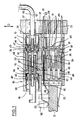
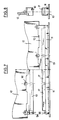
- FIG. 1 shows a connection assembly comprising a plug 10 and a base 11 for the electrical connection of electrical tracks formed respectively on a daughter board 12 and a mother board 13.
- the plug 10 comprises a hollow peripheral frame of rectangular section 14 in which a block of insulating material 16 is received.
- the insulating block 16 receives in small cells of the female electrical contact elements 18 allowing for example the transmission of an electrical signal.
- the electrical contact elements 18 protrude axially beyond the rear face 20 of the plug insulating block 16 to be connected to one of the faces of the motherboard 12 by means of connection grids 22 whose ends are elastically plated on the opposite faces of the daughter card 12 to allow connection according to the so-called flat transfer technique.
- the front ends 24 of the contacts 18 project axially beyond the front face 26 of the block insulator 16 towards the base 11.
- the insulating block 16 has in its middle part a through slot 28 which receives a ground connection strip 30, the front end 32 of which projects axially in the direction of the base 11 beyond the front face 26 of the block 16.
- a large cell 34 formed at the top of the insulating block 16 receives a female coaxial contact, the rear part of which is maintained and immobilized in a large cell 36 of the plug frame 14 which extends the cell 34 of block 16.
- the female coaxial contact 38 is mounted from the rear in the plug 10 and is immobilized there axially in the direction of the rear by a retaining ring 40 comprising elastically deformed fingers radially inwardly which cooperate with a retaining shoulder 42 of the external contact body of the female coaxial contact 38.
- the axial position of the plug connection module constituted by the insulating block 16 and by the electrical contacts which equip it is defined by an internal shoulder 44 of the plug body against which an external shoulder 46 of the insulating body 16 of the module is supported. plug, by a transverse face of the shoulder facing the rear connection face 20 of the block 16.
- the plug frame 14 extends axially forwards via its front end side wall 48 beyond the front connection face 26 of the block 16 to delimit a receptacle of rectangular section intended to receive a part of complementary shape of the insulating block of the plug 11.
- the base 11 symmetrically comprises a peripheral frame of rectangular section 15 in which is received a base insulating block 17.
- Small cells receive three male electrical contact elements 19 provided for cooperating electrically by their front ends 25 with the front ends 24 of the female contacts 18.
- the male signal electrical contacts 19 extend axially towards the rear of the base 11 beyond the rear connection face 21 of the insulating block 17 to penetrate corresponding tapping holes 23 of the motherboard 13.
- the front face of connection 27 of the insulating block of base 17 bears against the front face of connection 26 of the insulating block of plug 16, the front ends 25 of the female electrical contacts penetrating into corresponding cells of the insulating block 27 formed around the ends free before 25 of the male electrical contacts 19.
- the insulating base block 17 has a slot 29 in which a ground connection strip 31 is received, the front end of which in the form of a clamp 33 receives the front end 32 of the ground strip 30 of the plug 10.
- the insulating block 17 and the base frame 15 comprise large cells 35 and 37 which receive the rear part of the male coaxial contact 39 in which it is held axially towards the rear by an external ferrule to elastic fingers 41 which cooperate with a shoulder 43 of the contact body of the coaxial contact 39.
- the axial position of the base connection module constituted by the insulating block 17 and by the contacts which equip it is defined by a transverse partition 45 of the base frame 15 which constitutes an axial shoulder against which the rear face of connection 21 of the insulating block of base 17 or against a internal shoulder 47 of the base frame 15.
- the shoulders and surfaces thus in contact are turned towards the rear as regards the insulating block 17 so as to allow its axial introduction into the base frame 15 from the front towards the back.
- the partition 45 has slots 49 which extend perpendicular to the plane of the daughter board 12 and perpendicular to that of the mother board 13.
- the slots are thus oriented so as to allow, in a manner which will be explained below, a clearance of the connection assembly relative to the motherboard in the direction D parallel to the plane of the motherboard.
- the insulating block 17 of the base 11 extends axially forwards beyond the free front edge 51 of the base frame 15 to be received in the receptacle delimited by the front wall 48 of the plug frame 14.
- This arrangement eliminates the conventional guide between connectors in which a frame is received inside another frame. This saves twice the thickness of a front frame wall such as the wall 48, which makes it possible to increase the number of contacts for an external bulk of the determined frame. Guiding during nesting takes place between the insulating block and the front frame wall. It is thus also made possible to produce the plastic frames, such as the insulating blocks, and it is no longer necessary for the two frames to be metallic in order to withstand the forces during nesting.
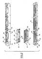
- the frame 14 constituting the body of the plug 10 comprises fixing lugs 50 on the card 12 by means of screws 52 as shown in FIG. 5.
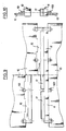
- each of the plug and socket frames is designed to receive three connection modules arranged side by side in three adjacent housings of each of the frames which are delimited by zones 54 and 55 respectively. It is in these zones 54 and 55 that the means for fixing the frames on their respective card are arranged, keying means, not shown and possibly means for locking the closure of the connection assembly.
- Each module in Figure 2 has 84 cells for electrical signal contacts and four larger cells which can receive either a coaxial contact as in Figure 1, or a power contact as in Figure 3, or an element called fluid contact, not shown in the figures, which makes it possible to circulate a heat transfer liquid.
- connection density of such modules it is possible to provide, for example, three electrical contact cells between the pairs of large cells 34 and 35, the corresponding cells being of course arranged opposite in the frames between the cells 36 and the cells 37.
- connection assemblies of smaller dimensions using the same connection modules by limiting the length of the frame to a single housing, that is to say for example substantially the left third of the frames 14 and 15 shown. in Figure 2.
- the design according to the invention makes it possible to assemble the signal contact elements and the ground strips in their respective insulating module as well as the connection grids, the pins of which are still connected together by banks, to form a module of connection which is then introduced into the corresponding frame until the shoulders bear axially delimiting their respective position.
- the male or female coaxial contacts are mounted from the rear in their corresponding sockets.
- the final connection between the insulating blocks 16 and 17 and the frames 14 and 15 is carried out by depositing in the area of the rear faces 20 and 21 a layer of adhesive material called "putting" as indicated by the letter P in Figures 4 , 5 and 6.
- small clearances 51 are formed which surround the rear part of the electrical contacts 19 and which can be filled with adhesive in a first step in order to immobilize the contacts relative to the block before the introduction of the connection module in the frame.
- connection assembly provision is made to allow movement in the direction D of the connection assembly with respect to the motherboard 13, in particular when the connection assembly and the daughter card 12 are pressed against a device. of heat absorption for cooling circuits called "thermal guide-card connectors".
- the rear parts of the male electrical contacts of the base 19 are received in slots in the base frame 15 in which they can move with slight deformation.
- the rear portions of the signal contacts which extend through the slots 49 are advantageously flattened portions of contact elements of sections. cylindrical and whose flattened faces are perpendicular to the direction of movement D.
- a clearance 53 is also formed around the mass strip 31 to allow transverse movement.
- connection assembly in direction D without damaging any of the components of the connection assembly, the means of fixing between the plug and the socket being also suitable. for this purpose.
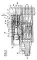
- the large cylindrical cells 35 to 37 also allow the mounting of power contacts as shown in FIG. 3.
- the male power contact 60 is mounted in the cells 34 and 36 in the same way as the male coaxial contact 38 in FIG. 1.
- the connection of its rear part, not shown, can be carried out by means of a flexible cable or by a curved end allowing it to be laid flat in the same way as the rear pins 22.
- the female contact 61 has a structure allowing its mounting from the rear and its partial disassembly for repair from the front as well as the transverse movement in the direction D.
- connection assembly shown in Figure 4 allows the connection of two motherboards parallel 12 and 13, the rear ends of the electrical signal contacts or of the coaxial contacts and of the power contacts being symmetrical, the other components of the plug 10 and of the socket 11 being similar to those of the embodiment shown in the preceding figures .
- connection assembly shown in FIG. 5 differs from that of FIG. 1 on the one hand in that it does not include ground connection strips, and on the other hand in that the connection grids 22 of the rear ends of the female contacts 18 of the plug 10 are connected to the card 12 by stitching into this card.
- a ground band could nevertheless be provided and overmolded as in the previous examples.
- a plug 64 can be molded in the insulating block 14 to close the slot 28 towards the rear.
- the base 11 is modified in its rear part to allow the connection of a daughter card 12 to an extension daughter card 13 in the extension of one another. That is to say to constitute a set called extension.
- the rear part of the extension base 11 is thus symmetrical to that of the plug shown in particular in FIGS. 1 and 2 and includes fixing lugs 100 on the second motherboard 13.
- a base forming an extension is shown in FIGS. 9 and 10 .
- all of the signal contacts of the plug 10 are female contacts while the contact elements of the base 11 are male contacts. It can be seen that by combining an extension base 11 as shown in FIG. 6 with a plug allowing the stitching such that shown in Figure 4, it is possible to reverse the direction of connection, that is to say, to equip the motherboard with female contacts and the daughter board with male contacts.
- connection assemblies A complete range of connection assemblies has thus been produced, making it possible to produce all the possible variants of links of printed circuit boards.
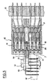
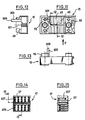
- FIGS. 11 to 13 show a lateral end of a base frame 15 which receives a base connection module 17 shown in FIGS. 14 and 15.
- the end zone 55 is in the form of a rectangular block, a side face 201 facing the housing of the insulating block 17 is provided with a coding finger 203.
- the finger extends from the front face of the partition 45 along the block 55 and projects axially beyond the free face of the latter.
- the lateral face 205 of the insulating block 17 which faces the face 201 has an axial groove 207 which receives the finger 203 and stiffens it.
- the finger 203 extends axially beyond the front face 27 of the insulating block 17 in the direction of the plug to be received in a keying hole of corresponding section formed in the side wall of the corresponding plug frame (not shown).
- An identical coding finger is arranged symmetrically at the other end of the base frame 15 as well as a corresponding hole in the plug frame.
- the fingers and holes are of course offset relative to the median plane of the frames to ensure the polarization function. It is not necessary to provide a lateral groove in the insulating block 16 of the plug because its front face 26 is set back from the free end 209 of the finger 203.
Landscapes
- Coupling Device And Connection With Printed Circuit (AREA)
- Details Of Connecting Devices For Male And Female Coupling (AREA)
- Multi-Conductor Connections (AREA)
Applications Claiming Priority (2)
| Application Number | Priority Date | Filing Date | Title |
|---|---|---|---|
| FR8907264A FR2647971B1 (fr) | 1989-06-01 | 1989-06-01 | Ensemble de connexion pour cartes a circuits imprimes |
| FR8907264 | 1989-06-01 |
Publications (2)
| Publication Number | Publication Date |
|---|---|
| EP0401121A1 true EP0401121A1 (de) | 1990-12-05 |
| EP0401121B1 EP0401121B1 (de) | 1994-08-31 |
Family
ID=9382273
Family Applications (2)
| Application Number | Title | Priority Date | Filing Date |
|---|---|---|---|
| EP90401470A Expired - Lifetime EP0401122B1 (de) | 1989-06-01 | 1990-05-31 | Element eines elektrischen Steckverbinders |
| EP90401469A Expired - Lifetime EP0401121B1 (de) | 1989-06-01 | 1990-05-31 | Verbindungszusammenbau für gedruckte Schaltungskarten |
Family Applications Before (1)
| Application Number | Title | Priority Date | Filing Date |
|---|---|---|---|
| EP90401470A Expired - Lifetime EP0401122B1 (de) | 1989-06-01 | 1990-05-31 | Element eines elektrischen Steckverbinders |
Country Status (5)
| Country | Link |
|---|---|
| US (1) | US5037314A (de) |
| EP (2) | EP0401122B1 (de) |
| DE (2) | DE69011958T2 (de) |
| ES (1) | ES2063304T3 (de) |
| FR (1) | FR2647971B1 (de) |
Cited By (3)
| Publication number | Priority date | Publication date | Assignee | Title |
|---|---|---|---|---|
| EP0607920A2 (de) * | 1993-01-19 | 1994-07-27 | The Whitaker Corporation | Elektrischer Verbinder für Stromversorgungs- und Signalkontakte |
| EP0704933A3 (de) * | 1994-09-30 | 1996-11-13 | Thomas & Betts Corp | Elektrischer Steckverbinder und dessen Herstellungsverfahren |
| US5709557A (en) * | 1994-12-12 | 1998-01-20 | The Whitaker Corporation | Electrical connector for dual printed circuit boards |
Families Citing this family (13)
| Publication number | Priority date | Publication date | Assignee | Title |
|---|---|---|---|---|
| JP2575617Y2 (ja) * | 1993-01-14 | 1998-07-02 | 矢崎総業株式会社 | 回路基板用コネクタ |
| FR2702888B1 (fr) * | 1993-03-16 | 1995-05-24 | Framatome Connectors France | Contact électrique pour connecteur et connecteur le comprenant. |
| US5397241A (en) * | 1993-10-25 | 1995-03-14 | At&T Corp. | High density electrical connector |
| US5472349A (en) * | 1994-10-31 | 1995-12-05 | The Whitaker Corporation | Surface mountable board edge connector |
| JP3505640B2 (ja) * | 1999-11-25 | 2004-03-08 | 日本航空電子工業株式会社 | フレキシブルな伝送線路一体型コネクタ |
| US6910897B2 (en) | 2001-01-12 | 2005-06-28 | Litton Systems, Inc. | Interconnection system |
| US6843657B2 (en) | 2001-01-12 | 2005-01-18 | Litton Systems Inc. | High speed, high density interconnect system for differential and single-ended transmission applications |
| US6979202B2 (en) | 2001-01-12 | 2005-12-27 | Litton Systems, Inc. | High-speed electrical connector |
| GR1006628B (el) | 2009-01-28 | 2009-12-11 | Αριστοτελειο Πανεπιστημιο Θεσσαλονικης-Ειδικος Λογαριασμος Αξιοποιησης Κονδυλιων Ερευνας | Μεθοδος και συστημα συνδυασμου σηματων με απουσια εκτιμησης κερδους καναλιων, για εφαρμογη σε δεκτες ασυρματων τηλεπικοινωνιακων συστηματων |
| DK2290753T3 (da) * | 2009-08-31 | 2013-03-18 | Erni Electronics Gmbh | Konnektor og flerlagsprintplade |
| DE202012008970U1 (de) * | 2012-09-18 | 2012-10-17 | Rosenberger Hochfrequenztechnik Gmbh & Co. Kg | Steckverbinder |
| US9048565B2 (en) * | 2013-06-12 | 2015-06-02 | Ironwood Electronics, Inc. | Adapter apparatus with deflectable element socket contacts |
| US9877404B1 (en) | 2017-01-27 | 2018-01-23 | Ironwood Electronics, Inc. | Adapter apparatus with socket contacts held in openings by holding structures |
Citations (2)
| Publication number | Priority date | Publication date | Assignee | Title |
|---|---|---|---|---|
| EP0152743A1 (de) * | 1984-01-27 | 1985-08-28 | Litton Precision Products International GmbH | Modularer elekrischer Steckverbinder |
| US4702707A (en) * | 1986-08-15 | 1987-10-27 | Amp Incorporated | Power contact having removable mating components |
Family Cites Families (8)
| Publication number | Priority date | Publication date | Assignee | Title |
|---|---|---|---|---|
| FR91750E (fr) * | 1966-01-27 | 1968-08-02 | Int Standard Electric Corp | Montage pour assurer un contact électrique |
| FR2550894B1 (fr) * | 1983-08-19 | 1985-10-11 | Socapex | Dispositif de connexion de circuits imprimes permettant l'enfichage d'une carte fille sur une carte mere |
| FR2582454B1 (fr) * | 1985-05-22 | 1989-07-21 | Lb Air | Dispositif de connexion electrique recevant des embouts de contact fixes a l'extremite de conducteurs electriques a connecter |
| US4697864A (en) * | 1986-06-19 | 1987-10-06 | Amp Incorporated | Printed circuit board receptacle for sealed connector |
| US4836791A (en) * | 1987-11-16 | 1989-06-06 | Amp Incorporated | High density coax connector |
| US4808115A (en) * | 1987-07-28 | 1989-02-28 | Amp Incorporated | Line replaceable connector assembly for use with printed circuit boards |
| DE8713932U1 (de) * | 1987-10-16 | 1988-01-14 | Du Pont De Nemours (Nederland) B.V., Dordrecht, Nl | |
| US4923405A (en) * | 1989-04-21 | 1990-05-08 | Chrysler Corporation | Printed circuit board, in line straight pin connector therefor |
-
1989
- 1989-06-01 FR FR8907264A patent/FR2647971B1/fr not_active Expired - Fee Related
-
1990
- 1990-05-17 US US07/525,371 patent/US5037314A/en not_active Expired - Lifetime
- 1990-05-31 EP EP90401470A patent/EP0401122B1/de not_active Expired - Lifetime
- 1990-05-31 EP EP90401469A patent/EP0401121B1/de not_active Expired - Lifetime
- 1990-05-31 DE DE69011958T patent/DE69011958T2/de not_active Expired - Fee Related
- 1990-05-31 DE DE9090401470T patent/DE69001042T2/de not_active Expired - Fee Related
- 1990-05-31 ES ES90401469T patent/ES2063304T3/es not_active Expired - Lifetime
Patent Citations (2)
| Publication number | Priority date | Publication date | Assignee | Title |
|---|---|---|---|---|
| EP0152743A1 (de) * | 1984-01-27 | 1985-08-28 | Litton Precision Products International GmbH | Modularer elekrischer Steckverbinder |
| US4702707A (en) * | 1986-08-15 | 1987-10-27 | Amp Incorporated | Power contact having removable mating components |
Cited By (4)
| Publication number | Priority date | Publication date | Assignee | Title |
|---|---|---|---|---|
| EP0607920A2 (de) * | 1993-01-19 | 1994-07-27 | The Whitaker Corporation | Elektrischer Verbinder für Stromversorgungs- und Signalkontakte |
| EP0607920A3 (en) * | 1993-01-19 | 1996-01-31 | Whitaker Corp | Electrical connector for power and signal contacts. |
| EP0704933A3 (de) * | 1994-09-30 | 1996-11-13 | Thomas & Betts Corp | Elektrischer Steckverbinder und dessen Herstellungsverfahren |
| US5709557A (en) * | 1994-12-12 | 1998-01-20 | The Whitaker Corporation | Electrical connector for dual printed circuit boards |
Also Published As
| Publication number | Publication date |
|---|---|
| DE69001042D1 (de) | 1993-04-15 |
| ES2063304T3 (es) | 1995-01-01 |
| EP0401122B1 (de) | 1993-03-10 |
| EP0401121B1 (de) | 1994-08-31 |
| EP0401122A1 (de) | 1990-12-05 |
| DE69011958T2 (de) | 1995-01-05 |
| US5037314A (en) | 1991-08-06 |
| FR2647971A1 (fr) | 1990-12-07 |
| DE69011958D1 (de) | 1994-10-06 |
| FR2647971B1 (fr) | 1991-09-20 |
| DE69001042T2 (de) | 1993-06-17 |
Similar Documents
| Publication | Publication Date | Title |
|---|---|---|
| EP0401121B1 (de) | Verbindungszusammenbau für gedruckte Schaltungskarten | |
| EP0942492B1 (de) | Gehäuse zur elektronischen Verbindung an einen Computer ausgerüstet mit einem IC-Karten-Verbinder | |
| EP0775375B1 (de) | Anspeisenetzwerk mit niedrigem übersprechen | |
| EP0578520B1 (de) | Modularer Einschub-Leiterplattenträger für Baugruppenträger | |
| EP0738429B1 (de) | Elektrischer verbinder für eine elektronische speicherkarte mit elektrischen isolationverdrängungsverbindern | |
| EP1028490A1 (de) | Koaxialverbinder zum Verbinden von zwei Leiterplatten | |
| EP0619625A1 (de) | Elektrischer Verbinder mit einer Anzahl von Modulen in Reihen und Kolonnen geordnet | |
| FR2749711A1 (fr) | Detrompage de connecteurs electriques | |
| FR2684242A1 (fr) | Assemblage de connecteur electrique comportant un element de verrouillage des bornes. | |
| EP2466692B1 (de) | Steckverbinder für Leiterplatte | |
| EP3687003B1 (de) | Steckverbinder für gedruckte schaltung, der mit einer leitenden hülle zum verschliessen einer übertragungsleitung für elektrische signale ausgestattet ist | |
| FR2666936A1 (fr) | Fiche isolante encliquetable dans un boitier de connecteurs electriques. | |
| EP0619626A1 (de) | Elektrischer Verbinder mit einer Anzahl von Steckmodulen | |
| FR2733358A1 (fr) | Connecteur electrique, notamment pour le raccordement d'une carte a memoire electronique | |
| FR2855710A1 (fr) | Unite electronique ainsi que procede permettant de fabriquer une unite electronique | |
| EP0078750A1 (de) | Flachverbinder für eine grosse Anzahl von Kontakten | |
| FR2700093A1 (fr) | Ensemble électronique fait de deux cartes réunies par des moyens d'assemblage et matériel électronique comportant au moins un tel ensemble. | |
| EP0534846B1 (de) | Elektrisches Verbindersystem für Flachkabel | |
| EP0560648B1 (de) | Polygonal Steckverbinder, insbesondere viereckig mit einem isolierenden Zentralkörper | |
| FR2521788A1 (fr) | Connecteur pour cartes a circuits imprimes | |
| FR2733363A1 (fr) | Procede de realisation d'un element modulaire de connexion electrique et element modulaire de connexion electrique ainsi obtenu | |
| EP0994529A1 (de) | Elektrischer Steckverbinder mit geringer Einsteck- und Herausziehkraft und C-förmigen Kontakten und Messerkontakten | |
| EP0821837B1 (de) | Miniatur koaxialschaltsteckverbinder mit betätigungsstift und passiven kontaktfedern | |
| FR2693845A1 (fr) | Connecteur électrique blindé perfectionné. | |
| FR2469016A1 (fr) | Dispositif de connexion electrique pour cables |
Legal Events
| Date | Code | Title | Description |
|---|---|---|---|
| PUAI | Public reference made under article 153(3) epc to a published international application that has entered the european phase |
Free format text: ORIGINAL CODE: 0009012 |
|
| AK | Designated contracting states |
Kind code of ref document: A1 Designated state(s): DE ES FR GB IT SE |
|
| 17P | Request for examination filed |
Effective date: 19901211 |
|
| 17Q | First examination report despatched |
Effective date: 19930818 |
|
| GRAA | (expected) grant |
Free format text: ORIGINAL CODE: 0009210 |
|
| AK | Designated contracting states |
Kind code of ref document: B1 Designated state(s): DE ES FR GB IT SE |
|
| REF | Corresponds to: |
Ref document number: 69011958 Country of ref document: DE Date of ref document: 19941006 |
|
| GBT | Gb: translation of ep patent filed (gb section 77(6)(a)/1977) |
Effective date: 19941004 |
|
| ITF | It: translation for a ep patent filed |
Owner name: BUGNION S.P.A. |
|
| REG | Reference to a national code |
Ref country code: ES Ref legal event code: FG2A Ref document number: 2063304 Country of ref document: ES Kind code of ref document: T3 |
|
| EAL | Se: european patent in force in sweden |
Ref document number: 90401469.3 |
|
| PLBE | No opposition filed within time limit |
Free format text: ORIGINAL CODE: 0009261 |
|
| STAA | Information on the status of an ep patent application or granted ep patent |
Free format text: STATUS: NO OPPOSITION FILED WITHIN TIME LIMIT |
|
| 26N | No opposition filed | ||
| REG | Reference to a national code |
Ref country code: GB Ref legal event code: IF02 |
|
| PGFP | Annual fee paid to national office [announced via postgrant information from national office to epo] |
Ref country code: FR Payment date: 20020501 Year of fee payment: 13 |
|
| PGFP | Annual fee paid to national office [announced via postgrant information from national office to epo] |
Ref country code: SE Payment date: 20020502 Year of fee payment: 13 |
|
| PGFP | Annual fee paid to national office [announced via postgrant information from national office to epo] |
Ref country code: DE Payment date: 20020520 Year of fee payment: 13 |
|
| PGFP | Annual fee paid to national office [announced via postgrant information from national office to epo] |
Ref country code: GB Payment date: 20020522 Year of fee payment: 13 |
|
| PGFP | Annual fee paid to national office [announced via postgrant information from national office to epo] |
Ref country code: ES Payment date: 20020606 Year of fee payment: 13 |
|
| PG25 | Lapsed in a contracting state [announced via postgrant information from national office to epo] |
Ref country code: GB Free format text: LAPSE BECAUSE OF NON-PAYMENT OF DUE FEES Effective date: 20030531 |
|
| PG25 | Lapsed in a contracting state [announced via postgrant information from national office to epo] |
Ref country code: SE Free format text: LAPSE BECAUSE OF NON-PAYMENT OF DUE FEES Effective date: 20030601 |
|
| PG25 | Lapsed in a contracting state [announced via postgrant information from national office to epo] |
Ref country code: ES Free format text: LAPSE BECAUSE OF NON-PAYMENT OF DUE FEES Effective date: 20030602 |
|
| PG25 | Lapsed in a contracting state [announced via postgrant information from national office to epo] |
Ref country code: DE Free format text: LAPSE BECAUSE OF NON-PAYMENT OF DUE FEES Effective date: 20031202 |
|
| GBPC | Gb: european patent ceased through non-payment of renewal fee |
Effective date: 20030531 |
|
| PG25 | Lapsed in a contracting state [announced via postgrant information from national office to epo] |
Ref country code: FR Free format text: LAPSE BECAUSE OF NON-PAYMENT OF DUE FEES Effective date: 20040130 |
|
| EUG | Se: european patent has lapsed | ||
| REG | Reference to a national code |
Ref country code: FR Ref legal event code: ST |
|
| REG | Reference to a national code |
Ref country code: ES Ref legal event code: FD2A Effective date: 20030602 |
|
| PG25 | Lapsed in a contracting state [announced via postgrant information from national office to epo] |
Ref country code: IT Free format text: LAPSE BECAUSE OF NON-PAYMENT OF DUE FEES Effective date: 20050531 |