EP0399616B1 - CVD reactor and method of using the same - Google Patents
CVD reactor and method of using the same Download PDFInfo
- Publication number
- EP0399616B1 EP0399616B1 EP90201297A EP90201297A EP0399616B1 EP 0399616 B1 EP0399616 B1 EP 0399616B1 EP 90201297 A EP90201297 A EP 90201297A EP 90201297 A EP90201297 A EP 90201297A EP 0399616 B1 EP0399616 B1 EP 0399616B1
- Authority
- EP
- European Patent Office
- Prior art keywords
- susceptor
- reactor
- susceptors
- gas
- wafer
- Prior art date
- Legal status (The legal status is an assumption and is not a legal conclusion. Google has not performed a legal analysis and makes no representation as to the accuracy of the status listed.)
- Expired - Lifetime
Links
Images



Classifications
-
- C—CHEMISTRY; METALLURGY
- C23—COATING METALLIC MATERIAL; COATING MATERIAL WITH METALLIC MATERIAL; CHEMICAL SURFACE TREATMENT; DIFFUSION TREATMENT OF METALLIC MATERIAL; COATING BY VACUUM EVAPORATION, BY SPUTTERING, BY ION IMPLANTATION OR BY CHEMICAL VAPOUR DEPOSITION, IN GENERAL; INHIBITING CORROSION OF METALLIC MATERIAL OR INCRUSTATION IN GENERAL
- C23C—COATING METALLIC MATERIAL; COATING MATERIAL WITH METALLIC MATERIAL; SURFACE TREATMENT OF METALLIC MATERIAL BY DIFFUSION INTO THE SURFACE, BY CHEMICAL CONVERSION OR SUBSTITUTION; COATING BY VACUUM EVAPORATION, BY SPUTTERING, BY ION IMPLANTATION OR BY CHEMICAL VAPOUR DEPOSITION, IN GENERAL
- C23C16/00—Chemical coating by decomposition of gaseous compounds, without leaving reaction products of surface material in the coating, i.e. chemical vapour deposition [CVD] processes
- C23C16/44—Chemical coating by decomposition of gaseous compounds, without leaving reaction products of surface material in the coating, i.e. chemical vapour deposition [CVD] processes characterised by the method of coating
- C23C16/455—Chemical coating by decomposition of gaseous compounds, without leaving reaction products of surface material in the coating, i.e. chemical vapour deposition [CVD] processes characterised by the method of coating characterised by the method used for introducing gases into reaction chamber or for modifying gas flows in reaction chamber
- C23C16/45563—Gas nozzles
- C23C16/45565—Shower nozzles
-
- C—CHEMISTRY; METALLURGY
- C23—COATING METALLIC MATERIAL; COATING MATERIAL WITH METALLIC MATERIAL; CHEMICAL SURFACE TREATMENT; DIFFUSION TREATMENT OF METALLIC MATERIAL; COATING BY VACUUM EVAPORATION, BY SPUTTERING, BY ION IMPLANTATION OR BY CHEMICAL VAPOUR DEPOSITION, IN GENERAL; INHIBITING CORROSION OF METALLIC MATERIAL OR INCRUSTATION IN GENERAL
- C23C—COATING METALLIC MATERIAL; COATING MATERIAL WITH METALLIC MATERIAL; SURFACE TREATMENT OF METALLIC MATERIAL BY DIFFUSION INTO THE SURFACE, BY CHEMICAL CONVERSION OR SUBSTITUTION; COATING BY VACUUM EVAPORATION, BY SPUTTERING, BY ION IMPLANTATION OR BY CHEMICAL VAPOUR DEPOSITION, IN GENERAL
- C23C16/00—Chemical coating by decomposition of gaseous compounds, without leaving reaction products of surface material in the coating, i.e. chemical vapour deposition [CVD] processes
- C23C16/44—Chemical coating by decomposition of gaseous compounds, without leaving reaction products of surface material in the coating, i.e. chemical vapour deposition [CVD] processes characterised by the method of coating
- C23C16/455—Chemical coating by decomposition of gaseous compounds, without leaving reaction products of surface material in the coating, i.e. chemical vapour deposition [CVD] processes characterised by the method of coating characterised by the method used for introducing gases into reaction chamber or for modifying gas flows in reaction chamber
-
- C—CHEMISTRY; METALLURGY
- C23—COATING METALLIC MATERIAL; COATING MATERIAL WITH METALLIC MATERIAL; CHEMICAL SURFACE TREATMENT; DIFFUSION TREATMENT OF METALLIC MATERIAL; COATING BY VACUUM EVAPORATION, BY SPUTTERING, BY ION IMPLANTATION OR BY CHEMICAL VAPOUR DEPOSITION, IN GENERAL; INHIBITING CORROSION OF METALLIC MATERIAL OR INCRUSTATION IN GENERAL
- C23C—COATING METALLIC MATERIAL; COATING MATERIAL WITH METALLIC MATERIAL; SURFACE TREATMENT OF METALLIC MATERIAL BY DIFFUSION INTO THE SURFACE, BY CHEMICAL CONVERSION OR SUBSTITUTION; COATING BY VACUUM EVAPORATION, BY SPUTTERING, BY ION IMPLANTATION OR BY CHEMICAL VAPOUR DEPOSITION, IN GENERAL
- C23C16/00—Chemical coating by decomposition of gaseous compounds, without leaving reaction products of surface material in the coating, i.e. chemical vapour deposition [CVD] processes
- C23C16/44—Chemical coating by decomposition of gaseous compounds, without leaving reaction products of surface material in the coating, i.e. chemical vapour deposition [CVD] processes characterised by the method of coating
- C23C16/54—Apparatus specially adapted for continuous coating
-
- H—ELECTRICITY
- H10—SEMICONDUCTOR DEVICES; ELECTRIC SOLID-STATE DEVICES NOT OTHERWISE PROVIDED FOR
- H10P—GENERIC PROCESSES OR APPARATUS FOR THE MANUFACTURE OR TREATMENT OF DEVICES COVERED BY CLASS H10
- H10P72/00—Handling or holding of wafers, substrates or devices during manufacture or treatment thereof
- H10P72/04—Apparatus for manufacture or treatment
- H10P72/0431—Apparatus for thermal treatment
- H10P72/0432—Apparatus for thermal treatment mainly by conduction
-
- H—ELECTRICITY
- H10—SEMICONDUCTOR DEVICES; ELECTRIC SOLID-STATE DEVICES NOT OTHERWISE PROVIDED FOR
- H10P—GENERIC PROCESSES OR APPARATUS FOR THE MANUFACTURE OR TREATMENT OF DEVICES COVERED BY CLASS H10
- H10P72/00—Handling or holding of wafers, substrates or devices during manufacture or treatment thereof
- H10P72/04—Apparatus for manufacture or treatment
- H10P72/0431—Apparatus for thermal treatment
- H10P72/0434—Apparatus for thermal treatment mainly by convection
Definitions
- the present invention relates to a CVD reactor having at least one station for processing at least one wafer and a method for processing multiple single wafers in a multi station CVD reactor.
- PECVD Plasma enhanced chemical vapor deposition
- PECVD reactors There are primarily three types of PECVD reactors: parallel plate, horizontal tube and single wafer.
- a parallel plate reactor the substrates or wafers are supported on a bottom grounded electrode and RF power is applied to an upper electrode.
- the grounded electrode may be rotated and heated to enhance uniformity.
- the reactant gas flow may be introduced centrally and removed peripherally or the reverse.
- a hollow tube PECVD reactor a plurality of vertically oriented electrodes are stacked parallel with one another with alternating plates serving as the power and ground electrodes for the applied RF energy.
- the wafers are interleaved with the electrodes. Generally, the entire assembly must be withdrawn from the tube for loading and unloading.
- a single wafer PECVD reactor may be load locked and offer cassette to cassette operation. Radiant heating of the wafer may be provided. The application of RF energy enhances the deposition process, as discussed above.
- An embodiment of this type of reactor includes a plurality of discrete gas dispersion heads disposed within a reactor for discharging a reactant gas to wafers disposed therebeneath upon a common plate. The use of such multiple heads provides a sequential station capability for deposition at each station.
- Another object of the present invention is to provide uniform radial flow of a reactant gas across a wafer in a reactor usable for PECVD, LPCVD or atmospheric CVD.
- Yet another object of the present invention is to provide reactant gas flow control to minimize residual deposits.
- Still another object of the present invention is to provide a single wafer plasma enhanced chemical vapor deposition reactor.
- a further object of the present invention is to provide apparatus for symmetrically distributing RF energy about a susceptor supported wafer.
- a still further object of the present invention is to provide rapid conductive heating of a wafer by a supporting susceptor.
- a yet further object of the present invention is to provide adjustment mechanisms for setting each susceptor and for mutually aligning each gas dispersion head with its associated susceptor within a reactor through an access opening of an otherwise closed reactor.
- a still further object of the present invention is to provide a method for controlling the flow of a reactant gas across the wafer during a CVD process.
- a yet further object of the present invention is to provide a method for increasing the throughput of a multi station wafer CVD processor.
- a still further object of the present invention is to provide a method for increasing the yield of a multi station CVD processor.
- a plurality of gas dispersion heads are vertically aligned with and set parallel to underlying heated wafer supporting susceptors.
- the combination of gas dispersion head configuration, parallelism between the gas dispersion head and the susceptor and downstream flow control provides a uniform outwardly radial gas flow along the wafer.
- a source of RF energy is electrically connected to the gas dispersion heads to concentrate an electrical plasma intermediate the gas dispersion heads and the respective susceptors whereby residual deposits within the chamber are minimized.
- a spider sequentially transports the wafers from susceptor to susceptor and a wafer handling apparatus, in combination with a load lock, replaces each processed wafer with an unprocessed wafer.
- FIG. 1 there is illustrated a reactor 10 constructed in accordance with the present invention. Under certain circumstances, a pair of reactors may be used at a work station, as illustrated.
- a port 12 of the reactor accommodates transport of the wafers into and out of the reactor.
- the port is in communication with a load lock apparatus 14 that includes a wafer handling mechanism 16.
- One or more input/output ports of which two (18,20) are shown receive cassettes 22 containing wafers to be processed and wafers which have been processed.
- the wafer handling mechanism transports each wafer from the respective input/output port through port 12 into reactor 10.
- the wafer handling mechanism retrieves the processed wafer from the reactor through port 12 and deposits it in the respective cassette located within a respective input/output port.
- Reactor 10 includes a plurality of equiangularly circularly arranged susceptors 30 for supporting respective ones of the wafers to be processed.
- a gas dispenser head 32 which is often referred to as a “shower head" is located vertically above and aligned with each susceptor.
- Each shower head is supported at the extremity of a radially extending hollow arm 34.
- Each arm is supported by and in fluid communication with a reactant gas distribution manifold, which manifold is connected to a source of reactant or other gas.
- a centrally located disk 36 includes a plurality of pairs of stalks; each pair of stalks supports a wafer during sequential transport of all of the wafers from one susceptor to an adjacent susceptor.
- Cover 38 of the reactor includes a plurality of removable hatches 40 to provide access to each susceptor/showerhead combination and to permit alignment and other adjustments after closing of the reactor.
- a single wafer etch module 24 may be incorporated, as illustrated.
- Manifold 50 interconnecting each of arms 34, is in fluid communication with conduit 52 extending upwardly from cover 38 of the reactor.
- the conduit is connected via valves to a source of reactant gas and other gases, as is well known in the art.
- Manifold 50 distributes the flow of gas to each of arms 34 at a predetermined rate in accordance with preset parameters.
- a junction block 54 disposed at the extremity of arm 34 supports shower head 32 via a hollow bellows 56 while providing fluid communication between the arm and the interior of the shower head.
- Susceptor 30 includes a depending shaft 58. Because of the configuration of the susceptor and its shaft, it is sometimes referred to as a "mushroom".
- the shaft extends through aperture 60 concentric therewith and formed in plate 62.
- the shaft extends further downwardly through a passageway disposed in bottom plate 64 of reactor 10.
- the shaft is sealingly but not rigidly disposed within the passageway.
- a suppressor 66 may be secured to bottom plate 64 via flange 68 and bolts 70 to receive the depending end of shaft 58 for purposes of reducing radio frequency interference.
- Plate 62 extends across reactor 10 and is supported upon a shoulder 76. The plate is secured upon the shoulder by a plurality of bolts 78 and means for effecting a seal between plate 62 and shoulder 76 may be employed.
- Exhaust chamber 78, formed between plate 62 and bottom plate 64 is in fluid communication with outlet 80 formed in the bottom plate.
- a downwardly depending conduit 82 is secured about outlet 80 by retention means 84.
- An exhaust pipe assembly 86 in fluid communication with conduit 82, conveys the exhausted reactant gas and other gases from reactor 10.
- a spider assembly 100 includes disk 36 supported upon a shaft 102.
- the shaft is disposed generally concentric with conduit 82.
- Positioning means 104 which may be disposed at the lower end of conduit 82, vertically repositions shaft 102 to raise and lower spider 100; furthermore, positioning means 104 will incrementally rotate the shaft on command to effect incremental angular repositioning about the vertical axis of spider 100.
- the spider includes a pair of parallel rods 106,108 associated with each susceptor. In the lowered position of spider 100, these pairs of rods rest within commensurately configured grooves formed in the upper surface of each respective susceptor.
- An RF generator 120 may be mounted upon cover 38 to provide a source of RF energy.
- item 120 may be an RF matching network with possibly more than one RF power input for multiple frequency operation.
- the RF energy is transmitted to manifold 50 via an electrically insulated conductor 122.
- Each of arms 34, junction blocks 54, bellows 56 and shower heads 32 are of electrically conductive material whereby each shower head serves as an electrode.
- the intensity of the radiant energy plasma therebetween can be regulated. Such regulation permits control of the distribution of radiant energy between the shower head and the susceptor.
- the intensity of radiant energy within the reactor exclusive of the electrical plasma intermediate the shower head and the susceptor can be minimized.
- the power level of the RF energy can also be varied. Through such reduction of ambient radiant energy, residual deposition within the reactor is substantially reduced.
- suppressor 66 may be used to eliminate spurious radiation exterior of reactor 10.
- a hatch 40 is detachably attachable to cover 38 by fastening means 128. Each hatch overlies an opening 130 in cover 38, which opening is generally coincident with the vertical axis of the underlying shower head and susceptor combination. Through this opening, adjustments to align and calibrate the various components may be made.
- Junction block 54 includes a laterally extending flange 140 having three threaded generally equiangularly displaced apertures 142 disposed proximate the perimeter of the flange.
- An adjustment screw 144 threadedly engages and depends from each threaded aperture 142 and is in pressure contact with upper surface 146 of shower head 32.
- Bellows 56 includes a coil spring 148 for drawing the shower head upwardly toward the junction block.
- Sleeve ends 150,152, extending in opposed directions from bellows 56, are attached to mounting plates 154,156, respectively.
- Mounting plate 154 is secured to flange 140 and an O-ring 158 may be employed to prevent leakage therebetween.
- Mounting plate 156 is secured to shower head 32 and O-ring 160 may be employed to prevent leakage therebetween.
- shower head 32 includes a cylindrical cavity 166, which cavity may include a cone shaped upper end section to assist in radially dispersing the reactant gas flowing thereinto from within bellows 56, as indicated by arrows 170.
- a diffusion plate 172 having a multiplicity of apertures 174 extends across the lower end of cavity 166. The diffusion plate may be secured in place by a ring 176.
- the reactant gas flowing into cavity 166 is dispersed through apertures 174 downwardly toward wafer 180 and radially outwardly therealong, as depicted by arrows 182.
- Susceptor 30 includes an inverted can like structure, preferably of aluminum or other thermal conducting material, having a relatively thick base 186 and a cylindrical sidewall 188.
- An electrically energized heater ring 190 is located adjacent the underside of base 186. It is retained in place by a retention ring 192 secured to the base via bolt means 194.
- An electrical conductor 196 extends from heater ring 190, through shaft 58 to a source of electrical energy for providing electrical power to the heater ring.
- a bottom cover plate 198 is retained in side wall 188 and bears against a radial flange 200.
- Shaft 58 is welded or othervise penetrably secured within central aperture 202 disposed within bottom plate 198.
- a thermal insulating composition 204 is disposed within the remaining space intermediate bottom plate 198 and base 186 to reduce heat transfer to the bottom plate and the depending side wall.
- a thermocouple 206 is disposed in a cavity 208 in base 186 to provide temperature related information via an electrical conductor 209 extending through shaft 58.
- Three threaded stanchions 210 extend upwardly from plate 62 to support susceptor 30 and to secure the susceptor to the plate.
- Adjustment/lock means such as an adjustment/lock nut 212, is associated with each stanchion to permit horizontal alignment and vertical positioning of the susceptor. It is to be understood that the stanchions also maintain the susceptor securely attached to plate 62.
- Aperture 60 formed in plate 62, is concentric with shaft 58 and dimensioned to provide an annular passageway for the flow of partially or fully depleted reactant gas, as indicated by arrows 216, into exhaust chamber 78 formed by plate 62 and bottom plate 64.
- each susceptor is, as described above, supported on plate 62.
- This plate has substantially equal pressure acting upon its top and bottom surfaces. Therefore, it will remain rigid and planar prior to and during operation of the reactor. Accordingly, alignment of the supported susceptors will not be altered in response to or as a consequence of a change in pressure within the reactor.
- passageway 220 extending through the bottom plate for penetrably receiving shaft 58 is sufficiently larger in diameter than the shaft to permit bowing of the bottom plate without having the wall of passageway 220 contact the shaft.
- an O-ring 222 is disposed about the shaft adjacent under surface 224 of bottom plate 64. The O-ring is retained in place by a collar 226.
- a seal of this type is effective in maintaining the interior of reactor 10 at its operating pressure and yet vertical movement and angular realignment of shaft 58 will be accommodated in response to manipulation of stanchions 210 and adjustment/lock means 212.
- Reactor 10 includes a cylindrical side wall 230 interconnecting cover 38 and bottom plate 64. Necessarily, an O-ring 232 or similar sealing means is disposed between the cylindrical side wall and the bottom plate. Further O-ring 234 or other sealing means is disposed intermediate the cylindrical side wall and the cover to effect a seal therebetween.
- One or more viewing ports having a transparent window 238 of quartz or other compatible material may be formed in cylindrical side wall 230. This viewing port may be employed for alignment and adjustment purposes of the shower head and the susceptor; it may be used to view the deposition process in effect upon wafer 180, for in situ measurements or for diagnostic purposes.
- Cover 38 may include an inverted U shaped bracket 240 for handling and support purposes.
- a support shroud 242 is attached to and extends upwardly from the center of cover 38 to support conduit 52 and provide support therefor.
- the support shroud can also provides fluid communication intermediate the bore of ceramic cylinder 124 and conduit 52.
- Annular sealing means, such as O-ring 244, is disposed between the support shroud and the cover to prevent leakage therebetween.
- the spider mounted upon vertically positionable and incrementally rotatable shaft 102 (see Figure 2) may include a single disk or a pair of parallel spaced apart disks for supporting pairs of stalks 106,108. These stalks are secured by positioning means, such as machine screws 110, to locate and maintain the stalks parallel and equispaced on opposed sides of a diametric line of disk 100.
- Base 186 of each suaceptor 30 includes a pair of grooves 250,252 disposed in upper surface 254. These grooves are in alignment with the respective pair of stalks 106,108. Moreover, the grooves are somewhat wider than the width of the stalks to permit some angular positioning tolerance of disk 36. The grooves are somewhat deeper than the height of the stalks to permit wafer 180 to lie flat upon surface 254 of the susceptor when spider 100 is in its lowered position.
- spider 100 is raised resulting in commensurate vertical repositioning of pairs of stalks 106,108. Each pair of rising stalks will lift up any overlying wafer. Necessarily, the pairs of stalks must extend a sufficient distance under each respective wafer to provide an adequate and balanced lifting force to prevent inadvertent radially outward tilting of the wafer.
- positioning means 104 See Figure 2
- spider 100 is incrementally angularly rotated about the vertical axis to position each pair of stalks in an overhead position with respect to an adjacent susceptor. Further actuation of positioning means 104 will lower the spider resulting in placement of the pair of stalks in grooves 250,252 of the adjacent susceptor.
- wafer handling mechanism 16 (see Figure 1) will enter reactor 10 through port 12 to withdraw a processed wafer from the susceptor in radial alignment with the port. After such withdrawal, the wafer handling mechanism will load a wafer to be processed upon the same susceptor still proximate port 12. Accordingly, after each phase or cycle of operation of reactor 10, a processed wafer is withdrawn.
- This withdrawal and loading capability provides a relatively rapid throughput not available from any of the prior art related reactors.
- the additional ports in the central loader (see Figure 1) permit the use of multiple parallel or sequential reactors. Necessarily, upon initial loading, a wafer is placed sequentially upon each susceptor and a cycle of the process can be performed intermediate each wafer loading.
- Conduit 52 in fluid communication with any of various sources of reactant or other gases, conveys the gas to manifold 50.
- Manifold 50 distributes the gases evenly into each of hollow equiangularly extending arms 34. From each arm, the gas is conveyed to cavity 66 in each of shower heads 32.
- Each diffusion plate 172 includes a plurality of apertures 174; the number, arrangement and size of these apertures may be varied, individually or collectively, to assist in providing better flow control of the gas across underlying wafer 180.
- bottom cover plate 198 will be substantially cooler than wafer supporting surface 254 and the likelihood of residual deposit upon the underside of the susceptor is reduced.
- side wall 188 will exhibit a substantial temperature gradient from top to bottom and residual deposit upon the lower part of the side wall will be reduced.
- the electrical plasma is substantially less adjacent the underside of the susceptor and the susceptor side wall, which further reduces the likelihood of residual deposit.
- adjustment means as shown in Figure 6, are provided to position susceptor 30 as a reference and thereafter showerhead 32 is aligned therewith. Referring jointly to Figures 6 and 8, this alignment procedure will be described in further detail. As depicted in the superimposed view shown in Figure 8, each of hatches 40 is aligned with a showerhead/susceptor pair. Upon removal of a hatch by undoing fastening means 128, manual access to adjustment/lock means 212 attendant stanchions 210 of the susceptor is available. The susceptor can then be trued with respect to plate 62 by use of feeler gauges, positioning jigs, and the like and locked in place by adjustment/lock means 212.
- the shower head is aligned to locate the lower surface of diffusion plate 172 parallel with surface 254 of the susceptor.
- alignment is effected by turning one or more of the three adjustment screws 144 in combination with the use of feeler gauges, positioning jigs, or the like.
- the adjustment screws are locked by lock nuts 143.
- bottom plate 64 will bow as a result of the pressure differential between the interior of the reaction chamber and ambient pressure.
- cover 38 may bow.
- Such bowing of cover 38 will cause vertical repositioning of manifold 50 from which arms 34 extend.
- Such vertical repositioning of the arms will provide a commensurate and uniform vertical repositioning of each of the shower heads.
- the alignment between a shower head and its paired susceptor will remain constant because the bowing of cover 38 will not result in angular displacement of the vertical axis of manifold 50.
- the amount of bowing of cover 38 which will occur commensurate with certain pressure differences between the interior of reactor 10 and the ambient pressure can be determined. With such information, the initial vertical position of each shower head can be set such that upon bowing of cover 38, the shower head will be in the preferred vertical relationship with respect to its paired susceptor.
- the RF generator includes an electrically insulated conductor 280 penetrably extending through aperture 282 in cover 38. Necessarily, sealing means 284 must be employed to prevent gas flow intermediate the conductor and the aperture.
- One end of a flexible ribbon conductor 286 is electrically connected to terminal end 288 of conductor 280.
- the other end of the ribbon conductor is electrically connected to a post 290 extending from the underside of manifold 50.
- arms 34, bellows 56 and shower heads 32 are of conductive material, they form, as a unit, an electrode.
- Ceramic cylinder 124 interconnecting manifold 50 with conduit 52, electrically insulates the manifold from the conduit and cover 38.
- the reactor housing As the reactor housing is at ground potential, it serves as a second electrode.
- the configuration of the high throughput single wafer multistage processor described herein provides outstanding flow control of the reactant and other gases to achieve high deposition uniformity.
- Symmetric distribution of the RF energy is available by using physically matching mating pairs of shower heads and susceptors as the electrodes.
- the gas flow control downstream of the wafer encourages uniform radial outward flow across the wafer.
- each susceptor has its own heater, temperature variations between susceptors are readily achieved for particular processing recipes.
- the adjustment features available for both the susceptors and the showerheads insures rapid setup time and adjustment capability commensurate with the process to be performed or recipe to be followed. Because of the limited residual deposits that will occur as a result of the flow control achieved, self cleaning by etching is available.
- Flow pattern uniformity and temperature distribution uniformity are critical to low pressure chemical vapor deposition processes.
- the flow control available and temperature distribution through conduction at the base of the susceptor are sufficient to effect low pressure chemical vapor deposition (LPCVD) with the above described reactor. That is, plasma enhancement is not critical to operation of reactor 10 and the reactor can be used as a LPCVD processor.
- LPCVD low pressure chemical vapor deposition
Landscapes
- Chemical & Material Sciences (AREA)
- General Chemical & Material Sciences (AREA)
- Chemical Kinetics & Catalysis (AREA)
- Engineering & Computer Science (AREA)
- Materials Engineering (AREA)
- Mechanical Engineering (AREA)
- Metallurgy (AREA)
- Organic Chemistry (AREA)
- Chemical Vapour Deposition (AREA)
Description
- The present invention relates to a CVD reactor having at least one station for processing at least one wafer and a method for processing multiple single wafers in a multi station CVD reactor.
- Plasma enhanced chemical vapor deposition (PECVD) methods have been developed relatively recently. Little literature is publicly available and much of that is directed to well known chemistry usable with PECVD rather than being directed to practical high throughput apparatus for implementing the process. PECVD uses an RF induced gas discharge to transfer energy to the reactant gases which allows a substrate to remain at a lower temperature than other processes. Such lower substrate temperature is a significant advantage in that it permits a method of depositing films on substrates that do not have thermal stability to accept coating by other methods. Additionally, PECVD can enhance the deposition rate when compared to thermal reactions alone and produce films of unique compositions and properties. Because of properties such as good adhesion, low pinhole density, good step coverage, adequate electrical properties and compatibility with fine line pattern transfer processes, this process has been used in integrated circuit manufacturing
- There are primarily three types of PECVD reactors: parallel plate, horizontal tube and single wafer. In a parallel plate reactor, the substrates or wafers are supported on a bottom grounded electrode and RF power is applied to an upper electrode. The grounded electrode may be rotated and heated to enhance uniformity. The reactant gas flow may be introduced centrally and removed peripherally or the reverse. In a hollow tube PECVD reactor, a plurality of vertically oriented electrodes are stacked parallel with one another with alternating plates serving as the power and ground electrodes for the applied RF energy. The wafers are interleaved with the electrodes. Generally, the entire assembly must be withdrawn from the tube for loading and unloading.
- A single wafer PECVD reactor may be load locked and offer cassette to cassette operation. Radiant heating of the wafer may be provided. The application of RF energy enhances the deposition process, as discussed above. An embodiment of this type of reactor includes a plurality of discrete gas dispersion heads disposed within a reactor for discharging a reactant gas to wafers disposed therebeneath upon a common plate. The use of such multiple heads provides a sequential station capability for deposition at each station.
- The chemistry and operating parameters attendant the process described below and related chemical vapor deposition (CVD) processes are described in detail in a textbook entitled Silicon Processing For the VLSI Era, Volume I - Process Technology, by S. Wolf and R.N. Tauber, published by the Lattice Press of Sunset Beach, California in 1987; chapters 5 and 6 are noted in particular. Further related information has been published in an article entitled "Chemical Vapor Deposition Techniques" by T.M. Besmann, D.P. Stinton and R.A. Lowden in the November 1988 issue of MRS Bulletin and references cited therein.
- It is therefore a primary object of the present invention to provide a multi station single wafer chemical vapor deposition processor.
- Another object of the present invention is to provide uniform radial flow of a reactant gas across a wafer in a reactor usable for PECVD, LPCVD or atmospheric CVD.
- Yet another object of the present invention is to provide reactant gas flow control to minimize residual deposits.
- Still another object of the present invention is to provide a single wafer plasma enhanced chemical vapor deposition reactor.
- A further object of the present invention is to provide apparatus for symmetrically distributing RF energy about a susceptor supported wafer.
- A still further object of the present invention is to provide rapid conductive heating of a wafer by a supporting susceptor.
- A yet further object of the present invention is to provide adjustment mechanisms for setting each susceptor and for mutually aligning each gas dispersion head with its associated susceptor within a reactor through an access opening of an otherwise closed reactor.
- A still further object of the present invention is to provide a method for controlling the flow of a reactant gas across the wafer during a CVD process.
- A yet further object of the present invention is to provide a method for increasing the throughput of a multi station wafer CVD processor.
- A still further object of the present invention is to provide a method for increasing the yield of a multi station CVD processor.
- The objects are realized with the apparatus according to claim 1 and the method according to claim 23.
- A plurality of gas dispersion heads are vertically aligned with and set parallel to underlying heated wafer supporting susceptors. The combination of gas dispersion head configuration, parallelism between the gas dispersion head and the susceptor and downstream flow control provides a uniform outwardly radial gas flow along the wafer. A source of RF energy is electrically connected to the gas dispersion heads to concentrate an electrical plasma intermediate the gas dispersion heads and the respective susceptors whereby residual deposits within the chamber are minimized. A spider sequentially transports the wafers from susceptor to susceptor and a wafer handling apparatus, in combination with a load lock, replaces each processed wafer with an unprocessed wafer.
- The present invention will be described with greater clarity and specificity with reference to the following drawings, in which:
- Figure 1 is a pictorial illustration of the major components of a multi station multi process CVD system for processing multiple single wafers;
- Figure 2 illustrates a partial cross sectional view of the CVD reactor;
- Figure 3 is a cross sectional view of the components of one of the stations within the reactor;
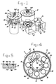
- Figure 4 is a top view of the wafer transporting spider;
- Figure 5 is a partial cross sectional view taken along lines 5-5, as shown in Figure 4;
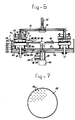
- Figure 6 is a partial cross sectional view of the reactor;
- Figure 7 is a view taken along line 7-7, as shown in Figure 6;
- Figure 8 is a partial top view of the reactor; and
- Figure 9 is a partial cross sectional view illustrating the RF generator and associated conductor.
- Referring to the pictorial illustration shown in Figure 1, there is illustrated a
reactor 10 constructed in accordance with the present invention. Under certain circumstances, a pair of reactors may be used at a work station, as illustrated. Aport 12 of the reactor accommodates transport of the wafers into and out of the reactor. The port is in communication with a load lock apparatus 14 that includes awafer handling mechanism 16. One or more input/output ports of which two (18,20) are shown, receivecassettes 22 containing wafers to be processed and wafers which have been processed. In operation, the wafer handling mechanism transports each wafer from the respective input/output port throughport 12 intoreactor 10. On completion of processing of a wafer, the wafer handling mechanism retrieves the processed wafer from the reactor throughport 12 and deposits it in the respective cassette located within a respective input/output port. -
Reactor 10 includes a plurality of equiangularly circularly arrangedsusceptors 30 for supporting respective ones of the wafers to be processed. Agas dispenser head 32, which is often referred to as a "shower head", is located vertically above and aligned with each susceptor. Each shower head is supported at the extremity of a radially extendinghollow arm 34. Each arm is supported by and in fluid communication with a reactant gas distribution manifold, which manifold is connected to a source of reactant or other gas. A centrally locateddisk 36 includes a plurality of pairs of stalks; each pair of stalks supports a wafer during sequential transport of all of the wafers from one susceptor to an adjacent susceptor.Cover 38 of the reactor includes a plurality ofremovable hatches 40 to provide access to each susceptor/showerhead combination and to permit alignment and other adjustments after closing of the reactor. Depending upon production requirements and other criteria, a singlewafer etch module 24 may be incorporated, as illustrated. - Particular features of
reactor 10 will be described with reference to Figure 2.Manifold 50, interconnecting each ofarms 34, is in fluid communication withconduit 52 extending upwardly fromcover 38 of the reactor. The conduit is connected via valves to a source of reactant gas and other gases, as is well known in the art.Manifold 50 distributes the flow of gas to each ofarms 34 at a predetermined rate in accordance with preset parameters. Ajunction block 54 disposed at the extremity ofarm 34 supportsshower head 32 via a hollow bellows 56 while providing fluid communication between the arm and the interior of the shower head.Susceptor 30 includes a dependingshaft 58. Because of the configuration of the susceptor and its shaft, it is sometimes referred to as a "mushroom". The shaft extends throughaperture 60 concentric therewith and formed inplate 62. The shaft extends further downwardly through a passageway disposed inbottom plate 64 ofreactor 10. The shaft is sealingly but not rigidly disposed within the passageway. Under certain circumstances, asuppressor 66 may be secured tobottom plate 64 via flange 68 and bolts 70 to receive the depending end ofshaft 58 for purposes of reducing radio frequency interference.Plate 62 extends acrossreactor 10 and is supported upon ashoulder 76. The plate is secured upon the shoulder by a plurality ofbolts 78 and means for effecting a seal betweenplate 62 andshoulder 76 may be employed.Exhaust chamber 78, formed betweenplate 62 andbottom plate 64, is in fluid communication with outlet 80 formed in the bottom plate. A downwardly dependingconduit 82 is secured about outlet 80 by retention means 84. Anexhaust pipe assembly 86, in fluid communication withconduit 82, conveys the exhausted reactant gas and other gases fromreactor 10. - A
spider assembly 100 includesdisk 36 supported upon ashaft 102. The shaft is disposed generally concentric withconduit 82. Positioning means 104, which may be disposed at the lower end ofconduit 82, vertically repositionsshaft 102 to raise andlower spider 100; furthermore, positioning means 104 will incrementally rotate the shaft on command to effect incremental angular repositioning about the vertical axis ofspider 100. The spider includes a pair of parallel rods 106,108 associated with each susceptor. In the lowered position ofspider 100, these pairs of rods rest within commensurately configured grooves formed in the upper surface of each respective susceptor. - An
RF generator 120 may be mounted uponcover 38 to provide a source of RF energy. Alternatively,item 120 may be an RF matching network with possibly more than one RF power input for multiple frequency operation. The RF energy is transmitted tomanifold 50 via an electricallyinsulated conductor 122. Aceramic collar 124, interconnectingmanifold 50 withcover 38 and providing for flow of gas therethrough, electrically isolates the manifold from the cover. Each ofarms 34, junction blocks 54, bellows 56 and shower heads 32 are of electrically conductive material whereby each shower head serves as an electrode.Susceptor 30, being grounded to both plate 62 (through adjustable supports as will be described below) andbottom plate 64, is at ground potential. By varying the distance betweenshower head 32 andsusceptor 30, the intensity of the radiant energy plasma therebetween can be regulated. Such regulation permits control of the distribution of radiant energy between the shower head and the susceptor. The intensity of radiant energy within the reactor exclusive of the electrical plasma intermediate the shower head and the susceptor can be minimized. As is well known, the power level of the RF energy can also be varied. Through such reduction of ambient radiant energy, residual deposition within the reactor is substantially reduced. - Under certain circumstances, it may be preferable to electrically isolate
susceptor 30 and maintain it at an above ground potential. Under such circumstances,suppressor 66 may be used to eliminate spurious radiation exterior ofreactor 10. - The positioning and alignment of
shower head 32 relative tosusceptor 30 is critical to uniform radial flow of the reactant gas upon the susceptor supported wafer. Moreover, the alignment therebetween will have a pronounced effect upon the distribution of the electrical plasma. Both the flow and the plasma have, in turn, a substantial effect upon the quality of wafer processing. To permit alignment and adjustment for these purposes, ahatch 40 is detachably attachable to cover 38 by fastening means 128. Each hatch overlies anopening 130 incover 38, which opening is generally coincident with the vertical axis of the underlying shower head and susceptor combination. Through this opening, adjustments to align and calibrate the various components may be made. - Further details relating to the shower head and the susceptor will be described with particular reference to Figure 3.
Junction block 54 includes a laterally extending flange 140 having three threaded generally equiangularly displaced apertures 142 disposed proximate the perimeter of the flange. Anadjustment screw 144 threadedly engages and depends from each threaded aperture 142 and is in pressure contact with upper surface 146 ofshower head 32.Bellows 56 includes a coil spring 148 for drawing the shower head upwardly toward the junction block. Sleeve ends 150,152, extending in opposed directions frombellows 56, are attached to mounting plates 154,156, respectively. Mounting plate 154 is secured to flange 140 and an O-ring 158 may be employed to prevent leakage therebetween. Mounting plate 156 is secured toshower head 32 and O-ring 160 may be employed to prevent leakage therebetween. -
Shower head 32 includes acylindrical cavity 166, which cavity may include a cone shaped upper end section to assist in radially dispersing the reactant gas flowing thereinto from withinbellows 56, as indicated by arrows 170. Adiffusion plate 172 having a multiplicity ofapertures 174 extends across the lower end ofcavity 166. The diffusion plate may be secured in place by a ring 176. The reactant gas flowing intocavity 166 is dispersed throughapertures 174 downwardly towardwafer 180 and radially outwardly therealong, as depicted by arrows 182. -
Susceptor 30 includes an inverted can like structure, preferably of aluminum or other thermal conducting material, having a relativelythick base 186 and acylindrical sidewall 188. An electrically energizedheater ring 190 is located adjacent the underside ofbase 186. It is retained in place by aretention ring 192 secured to the base via bolt means 194. An electrical conductor 196 extends fromheater ring 190, throughshaft 58 to a source of electrical energy for providing electrical power to the heater ring. A bottom cover plate 198 is retained inside wall 188 and bears against aradial flange 200.Shaft 58 is welded or othervise penetrably secured within central aperture 202 disposed within bottom plate 198. A thermal insulatingcomposition 204 is disposed within the remaining space intermediate bottom plate 198 andbase 186 to reduce heat transfer to the bottom plate and the depending side wall. A thermocouple 206 is disposed in acavity 208 inbase 186 to provide temperature related information via an electrical conductor 209 extending throughshaft 58. Three threadedstanchions 210 extend upwardly fromplate 62 to supportsusceptor 30 and to secure the susceptor to the plate. Adjustment/lock means, such as an adjustment/lock nut 212, is associated with each stanchion to permit horizontal alignment and vertical positioning of the susceptor. It is to be understood that the stanchions also maintain the susceptor securely attached toplate 62.Aperture 60, formed inplate 62, is concentric withshaft 58 and dimensioned to provide an annular passageway for the flow of partially or fully depleted reactant gas, as indicated byarrows 216, intoexhaust chamber 78 formed byplate 62 andbottom plate 64. - During processing, the interior of
reactor 10 is at a low, near vacuum, pressure; it may be in the range of 500 milli torr (1 torr = 133 Pa) to 5 torr but is typically at a pressure of 1½-2 torr. Because of the pressure differential between the interior of the reactor and the normal atmospheric pressure surrounding the reactor,plate 64 will bow. Weresusceptors 30 secured tobottom plate 64, the bowing of the bottom plate, during processing, would angularly realign and vertically reposition the susceptors. Such realignment and vertical repositioning, even though slight, would have a deleterious effect upon the uniformity of deposition on the wafer(s) being processed. To attempt to align or adjust accurately the susceptor to accommodate the expected, or even measured, bowing ofbottom plate 64 would be an almost impossible task and certainly it would be impossible to achieve the degree of alignment sought inreactor 10. To avoid this problem area, each susceptor is, as described above, supported onplate 62. This plate has substantially equal pressure acting upon its top and bottom surfaces. Therefore, it will remain rigid and planar prior to and during operation of the reactor. Accordingly, alignment of the supported susceptors will not be altered in response to or as a consequence of a change in pressure within the reactor. To permit bowing ofbottom plate 64 without affecting the alignment ofsusceptors 30,passageway 220 extending through the bottom plate for penetrably receivingshaft 58 is sufficiently larger in diameter than the shaft to permit bowing of the bottom plate without having the wall ofpassageway 220 contact the shaft. To seal the passageway, an O-ring 222 is disposed about the shaft adjacent undersurface 224 ofbottom plate 64. The O-ring is retained in place by acollar 226. A seal of this type is effective in maintaining the interior ofreactor 10 at its operating pressure and yet vertical movement and angular realignment ofshaft 58 will be accommodated in response to manipulation ofstanchions 210 and adjustment/lock means 212. -
Reactor 10 includes acylindrical side wall 230 interconnectingcover 38 andbottom plate 64. Necessarily, an O-ring 232 or similar sealing means is disposed between the cylindrical side wall and the bottom plate. Further O-ring 234 or other sealing means is disposed intermediate the cylindrical side wall and the cover to effect a seal therebetween. One or more viewing ports having atransparent window 238 of quartz or other compatible material may be formed incylindrical side wall 230. This viewing port may be employed for alignment and adjustment purposes of the shower head and the susceptor; it may be used to view the deposition process in effect uponwafer 180, for in situ measurements or for diagnostic purposes. -
Cover 38 may include an inverted U shapedbracket 240 for handling and support purposes. Asupport shroud 242 is attached to and extends upwardly from the center ofcover 38 to supportconduit 52 and provide support therefor. The support shroud can also provides fluid communication intermediate the bore ofceramic cylinder 124 andconduit 52. Annular sealing means, such as O-ring 244, is disposed between the support shroud and the cover to prevent leakage therebetween. - The structure and operation of
spider 100 will be described with particular reference to Figures 4 and 5. The spider, mounted upon vertically positionable and incrementally rotatable shaft 102 (see Figure 2) may include a single disk or a pair of parallel spaced apart disks for supporting pairs of stalks 106,108. These stalks are secured by positioning means, such asmachine screws 110, to locate and maintain the stalks parallel and equispaced on opposed sides of a diametric line ofdisk 100.Base 186 of each suaceptor 30 includes a pair of grooves 250,252 disposed inupper surface 254. These grooves are in alignment with the respective pair of stalks 106,108. Moreover, the grooves are somewhat wider than the width of the stalks to permit some angular positioning tolerance ofdisk 36. The grooves are somewhat deeper than the height of the stalks to permitwafer 180 to lie flat uponsurface 254 of the susceptor whenspider 100 is in its lowered position. - In operation, after each vapor deposition phase or cycle,
spider 100 is raised resulting in commensurate vertical repositioning of pairs of stalks 106,108. Each pair of rising stalks will lift up any overlying wafer. Necessarily, the pairs of stalks must extend a sufficient distance under each respective wafer to provide an adequate and balanced lifting force to prevent inadvertent radially outward tilting of the wafer. By further operation of positioning means 104 (see Figure 2),spider 100 is incrementally angularly rotated about the vertical axis to position each pair of stalks in an overhead position with respect to an adjacent susceptor. Further actuation of positioning means 104 will lower the spider resulting in placement of the pair of stalks in grooves 250,252 of the adjacent susceptor. Each wafer will then have been relocated to the next adjacent susceptor. Depending upon the cycling sequence, wafer handling mechanism 16 (see Figure 1) will enterreactor 10 throughport 12 to withdraw a processed wafer from the susceptor in radial alignment with the port. After such withdrawal, the wafer handling mechanism will load a wafer to be processed upon the same susceptor stillproximate port 12. Accordingly, after each phase or cycle of operation ofreactor 10, a processed wafer is withdrawn. This withdrawal and loading capability provides a relatively rapid throughput not available from any of the prior art related reactors. In particular, the additional ports in the central loader (see Figure 1) permit the use of multiple parallel or sequential reactors. Necessarily, upon initial loading, a wafer is placed sequentially upon each susceptor and a cycle of the process can be performed intermediate each wafer loading. - Referring to Figures 6 and 7, further details attendant the alignment capability and flow path control will be described. For sake of simplicity, certain details attendant earlier figures have been deleted.
Conduit 52, in fluid communication with any of various sources of reactant or other gases, conveys the gas tomanifold 50.Manifold 50 distributes the gases evenly into each of hollowequiangularly extending arms 34. From each arm, the gas is conveyed tocavity 66 in each of shower heads 32. Eachdiffusion plate 172 includes a plurality ofapertures 174; the number, arrangement and size of these apertures may be varied, individually or collectively, to assist in providing better flow control of the gas acrossunderlying wafer 180. The only outflow possible from within the space defined byside wall 230, cover 38 andplate 62 is viapassageway 60 surrounding eachshaft 58. Accordingly, the gas flow fromshower head 32 will flow downwardly towafer 180 and radially outwardly therealong to the circular edge ofsusceptor 30. The flow will be downwardlyadjacent side wall 188 and inwardly beneath bottom cover plate 198. From beneath the susceptor, the flow will be downwardly aboutshaft 58 throughpassageway 60. This flow pattern is depicted by arrows 260,262 and 264. Once the gas enters the space betweenplate 62 andbottom plate 64, it will flow radially inwardly intoexhaust pipe assembly 86 viaconduit 82. This flow is depicted by arrows 266,268,270,272 and 274. From this description, it will be evident that substantial control of the flow path of the gas is achieved. Moreover, the parameters controlling the flow path strongly discourage incidental and spurious flow within the reaction chamber. Thereby, residual deposits will be minimized. - It may be pointed out that due to the thermal insulation within
susceptor 30, described above, bottom cover plate 198 will be substantially cooler thanwafer supporting surface 254 and the likelihood of residual deposit upon the underside of the susceptor is reduced. Moreover,side wall 188 will exhibit a substantial temperature gradient from top to bottom and residual deposit upon the lower part of the side wall will be reduced. Moreover, the electrical plasma is substantially less adjacent the underside of the susceptor and the susceptor side wall, which further reduces the likelihood of residual deposit. - As previously described, adjustment means, as shown in Figure 6, are provided to position
susceptor 30 as a reference and thereafter showerhead 32 is aligned therewith. Referring jointly to Figures 6 and 8, this alignment procedure will be described in further detail. As depicted in the superimposed view shown in Figure 8, each of hatches 40 is aligned with a showerhead/susceptor pair. Upon removal of a hatch by undoing fastening means 128, manual access to adjustment/lock means 212attendant stanchions 210 of the susceptor is available. The susceptor can then be trued with respect to plate 62 by use of feeler gauges, positioning jigs, and the like and locked in place by adjustment/lock means 212. Once the susceptor is located as a reference, the shower head is aligned to locate the lower surface ofdiffusion plate 172 parallel withsurface 254 of the susceptor. Such alignment is effected by turning one or more of the threeadjustment screws 144 in combination with the use of feeler gauges, positioning jigs, or the like. When alignment is obtained, the adjustment screws are locked by lock nuts 143. - As discussed above,
bottom plate 64 will bow as a result of the pressure differential between the interior of the reaction chamber and ambient pressure. Similarly, cover 38 may bow. Such bowing ofcover 38 will cause vertical repositioning ofmanifold 50 from whicharms 34 extend. Such vertical repositioning of the arms will provide a commensurate and uniform vertical repositioning of each of the shower heads. However, the alignment between a shower head and its paired susceptor will remain constant because the bowing ofcover 38 will not result in angular displacement of the vertical axis ofmanifold 50. By experiment and/or calculation, the amount of bowing ofcover 38 which will occur commensurate with certain pressure differences between the interior ofreactor 10 and the ambient pressure can be determined. With such information, the initial vertical position of each shower head can be set such that upon bowing ofcover 38, the shower head will be in the preferred vertical relationship with respect to its paired susceptor. - Referring to Figure 9, there is shown further detail attendant the electrical connection between
RF generator 120 andmanifold 50. The RF generator includes an electricallyinsulated conductor 280 penetrably extending throughaperture 282 incover 38. Necessarily, sealing means 284 must be employed to prevent gas flow intermediate the conductor and the aperture. One end of aflexible ribbon conductor 286 is electrically connected toterminal end 288 ofconductor 280. The other end of the ribbon conductor is electrically connected to apost 290 extending from the underside ofmanifold 50. As the manifold,arms 34, bellows 56 and shower heads 32 are of conductive material, they form, as a unit, an electrode.Ceramic cylinder 124, interconnectingmanifold 50 withconduit 52, electrically insulates the manifold from the conduit and cover 38. As the reactor housing is at ground potential, it serves as a second electrode.Susceptor 30, being mechanically and electrically connected with the housing of the reactor, will be at ground potential. Because of the relatively small spacing between the susceptor and the shower head during operation of the reactor, a substantial electrical gradient and electrical plasma will exist between the shower head and the susceptor. This electrical plasma will enhance the rapidity and uniformity of deposition. Moreover, because of the dimensional equivalence betweensurface 254 of the susceptor and the bottom of the shower head, the RF distribution therebetween is optimized for enhanced uniformity in excitation of the reactant gas. The RF energy present elsewhere withinreactor 10 will be at a substantially reduced intensity and residual deposits will be minimal. - In summary, the configuration of the high throughput single wafer multistage processor described herein provides outstanding flow control of the reactant and other gases to achieve high deposition uniformity. Symmetric distribution of the RF energy is available by using physically matching mating pairs of shower heads and susceptors as the electrodes. The gas flow control downstream of the wafer encourages uniform radial outward flow across the wafer. As each susceptor has its own heater, temperature variations between susceptors are readily achieved for particular processing recipes. The adjustment features available for both the susceptors and the showerheads insures rapid setup time and adjustment capability commensurate with the process to be performed or recipe to be followed. Because of the limited residual deposits that will occur as a result of the flow control achieved, self cleaning by etching is available.
- Flow pattern uniformity and temperature distribution uniformity are critical to low pressure chemical vapor deposition processes. The flow control available and temperature distribution through conduction at the base of the susceptor are sufficient to effect low pressure chemical vapor deposition (LPCVD) with the above described reactor. That is, plasma enhancement is not critical to operation of
reactor 10 and the reactor can be used as a LPCVD processor.
Claims (35)
- CVD reactor having at least one station for processing at least one wafer, said reactor comprising in combination:a) at least one susceptor (30) for supporting a single wafer (180), the number of said susceptors being commensurate with the number of stations within said reactor;b) associated with each susceptor, a gas dispersions head (32) positioned above its associated susceptor for dispersing a gas upon an associated susceptor-supported wafer, said gas dispersionhead having its central axis aligned with the central axis of the susceptor, the lower surface of said gas dispersion head being parallel with the surface of its associated susceptor, andc) gas exhaust means downstreamof said susceptor for drawing the gas radially from the perimeter of the wafer.
- Reactor according to claim 1 including means (190) disposed in each of said susceptors for heating the wafer supported thereon.
- Reactor according to claim 1 or 2 including means (120) for irradiating with RF energy the gas flowing across the supported wafer.
- Reactor according to one of the preceding claims wherein said reactor includes a plate (64) spaced from said susceptor (30), a further plate (62) located intermediate said plate and said susceptors (30) for defining an exhaust chamber (78) between said plate and said further plate, an exhaust pipe assembly (86) for drawing gas from said exhaust chamber and passageway means disposed in said further plate for channelling flow of the gas from each of the supported wafers and through said further plate at a location proximate each of said susceptors and into said exhaust chamber.
- Reactor according to claim 4 wherein each of said susceptors (30) is circular in planform with a vertical axis of rotation and each of said susceptors including a downwardly extending axially aligned shaft (58) penetrably engaging said further plate (62) and wherein said passageway means comprises an annular passageway disposed about said shaft.
- Reactor according to claim 5 wherein said plate includes an aperture (60) for accomodating penetretion of said shaft and bowing of said plate without inducing commensurate repositioning of said shaft and seal means for sealing the junction between said shaft and said plate.
- Reactor according to one of the preceding claims in combination with claim 2 wherein each of said susceptors includes a hollow shaft (58) for housing electrical conductors (196) extending from said heating means.
- Reactor according to claim 7 including temperature sensing means (206) disposed in each of said susceptors and means (209) for conveying the temperature sensed through the bore of said shaft.
- Reactor according to one of the preceding claims, in combination with claim 4 wherein said reactor includes a cover, a plate, a sidewall interconnecting said cover and said plate, a further plate displaced from said plate for defining an exhaust chamber between said plate and said further plate, means for supporting each of said susceptors upon said further plate and means for suspending of said gas dispersion heads from said cover.
- Reactor according to claim 9 including first means (210, 212) for positionally adjusting each of said susceptors upon said further plate, second means (142, 143) for positionally adjusting each of said gas dispersion heads with respect to the associated one of said susceptors and access means for accommodating manipulation of said first and second adjusting means.
- Reactor according to claim 10 wherein said access means comprises at least one opening in said cover, each of said openings (130) being associated with said susceptors and the associated one of said gas dispersion heads and a removable hatch (40) for openably covering and sealing each of said openings.
- Reactor according to claim 10 or 11 wherein said suspending means comprises a plurality of radially extending arms (34) suspended from said cover, the number of said arms being equal to the number of said susceptors, each of said arms including means for supporting one of said gas dispersion heads and wherein said supporting means includes said second adjusting means.
- Rector according to claim 12 wherein each of said arms includes means for conveying the gas from a source of gas to the respective one of said gas dispersion heads.
- Reactor according to in claim 13 including a source of RF energy (120) and means for irradiating each wafer with RF energy from said source.
- Reactor according to claim 14 wherein each of said gas dispersion heads comprises one electrode (290) electrically connected to said RF source and wherein each of said susceptors comprises another electrode electrically connected to said RF source.
- Reactor according to one of the preceding claims including a plurality of said susceptors disposed circularly within said reactor.
- Reactor according to claim 16 including means for suspending from a common point each of said gas dispersion heads above the respective ones of said plurality of susceptors.
- Reactor according to claim 17 including a source of RF energy and wherein said plurality of gas dispersion heads comprises an electrode electrically connected to said RF source for irradiating the gas flowing across the wafer of the respective one of said plurality of susceptors.
- Reactor according to one of the claims 16-18 including a spider for transporting each of the wafers sequentially from one susceptor to an adjacent susceptor of said plurality of susceptors on completion of a cycle of the CVD process being performed.
- Reactor according to claim 19 wherein said spider (100) includes a plurality of pairs of rods (106, 108) for supporting the wafers during transport, each pair of said pairs of rods being associated with one susceptor of said plurality of susceptors.
- Reactor according to claim 20 wherein said spider is vertically repositionable to raise and lower the wafers and angularly repositionable to align sequentially said pairs of rods with said plurality of susceptors.
- Reactor according to claim 21 wherein each susceptor of said plurality of susceptors includes a pair of grooves for receiving a pair of said plurality of pairs of rods.
- Method for processing multiple single wafers in a multi station CVD reactor having a number of susceptors equal in number to the number of stations, said method comprising the steps of:a) supporting one wafer on a susceptor;b) dispersing a gas upon the supported wafer from a gas dispersion head associated with each susceptor positioned above its associated susceptor for dispersing a gas upon an associated susceptor-supported wafer, said gas dispersion head having its central axis aligned with the central axis of the susceptor and the lower surface of said gas dispersion head being parallel with the surface of its associated susceptor andc) exhausting the gas downstream of the wafer so as to urge outward radial flow of the gas across each supported wafer to the peripheral edge of the wafer.
- Method according to claim 23 including the step of heating the wafer with heat generated by the susceptor.
- Method according to claim 23 or 24 including the step of irradiating the wafer with RF energy.
- Method according to claim 25 including the step of radiating RF energy from the gas dispersion head to the susceptor.
- Method according to claim 26 including the step of drawing the gas from the perimeter of the wafer along the side of the susceptor and into and exhaust chamber having an opening centrally aligned with the susceptor.
- Method according to one of the claims 23-27 including a first step of adjusting and aligning the susceptor, a second step of adjusting and aligning the gas dispersion head relative to its association susceptor, and the step of performing said first end second adjusting and aligning steps through an openably closeable opening in the reactor and after assembly of the reactor.
- Method according to one of the claims 23-28 wherein a plurality of susceptors, each with an associated gas dispersion head, are located circularly within the reactor and including the step of sequentially repositioning the wafers from one susceptor to another susceptor.
- Method according to claim 29 including the step of loading unprocessed wafers within the reactor.
- Method according to one of the claims 29, 30 including the step of withdrawing processed wafers from the reactor.
- Method according to one of the claims 28-31 wherein said step of repositioning is performed on completion of each process cycle.
- Method according to one of the claims 23-32 including the step of loading a wafer into the reactor prior to initiation of a process cycle.
- Method according to one of the claims 23-33 including the step of radiating RF energy from each of the gas dispersion heads to irradiate the gas flowing from each of the gas dispersion heads and across the wafer supported on the associated susceptor.
- Method according to claim 34 including a first step of adjusting and aligning each susceptor, a second step of adjusting and aligning the gas dispersion head relative to its associated susceptor and the step of performing said first and second adjustment and aligning steps through at least one openably closeable opening in the reactor after assembly of the reactor.
Applications Claiming Priority (2)
| Application Number | Priority Date | Filing Date | Title |
|---|---|---|---|
| US07/354,922 US4987856A (en) | 1989-05-22 | 1989-05-22 | High throughput multi station processor for multiple single wafers |
| US354922 | 1989-05-22 |
Publications (2)
| Publication Number | Publication Date |
|---|---|
| EP0399616A1 EP0399616A1 (en) | 1990-11-28 |
| EP0399616B1 true EP0399616B1 (en) | 1997-08-06 |
Family
ID=23395465
Family Applications (1)
| Application Number | Title | Priority Date | Filing Date |
|---|---|---|---|
| EP90201297A Expired - Lifetime EP0399616B1 (en) | 1989-05-22 | 1990-05-22 | CVD reactor and method of using the same |
Country Status (4)
| Country | Link |
|---|---|
| US (1) | US4987856A (en) |
| EP (1) | EP0399616B1 (en) |
| JP (1) | JP3178824B2 (en) |
| DE (1) | DE69031192T2 (en) |
Families Citing this family (521)
| Publication number | Priority date | Publication date | Assignee | Title |
|---|---|---|---|---|
| KR0170391B1 (en) * | 1989-06-16 | 1999-03-30 | 다카시마 히로시 | Object processing device and processing method |
| DE4005956C1 (en) * | 1990-02-26 | 1991-06-06 | Siegfried Dipl.-Ing. Dr. 5135 Selfkant De Straemke | |
| US5147498A (en) * | 1990-04-09 | 1992-09-15 | Anelva Corporation | Apparatus for controlling temperature in the processing of a substrate |
| US5071670A (en) * | 1990-06-11 | 1991-12-10 | Kelly Michael A | Method for chemical vapor deposition under a single reactor vessel divided into separate reaction chambers each with its own depositing and exhausting means |
| US5260236A (en) * | 1991-06-07 | 1993-11-09 | Intel Corporation | UV transparent oxynitride deposition in single wafer PECVD system |
| US6004885A (en) * | 1991-12-26 | 1999-12-21 | Canon Kabushiki Kaisha | Thin film formation on semiconductor wafer |
| DE4143177C2 (en) * | 1991-12-30 | 1999-08-12 | Leybold Ag | Coating system |
| USH1373H (en) * | 1992-04-06 | 1994-11-01 | American Telephone And Telegraph Company | Wafer handling apparatus and method |
| US5338362A (en) * | 1992-08-29 | 1994-08-16 | Tokyo Electron Limited | Apparatus for processing semiconductor wafer comprising continuously rotating wafer table and plural chamber compartments |
| JPH0810678B2 (en) * | 1992-10-27 | 1996-01-31 | 株式会社半導体プロセス研究所 | Semiconductor device manufacturing equipment |
| JPH0828333B2 (en) * | 1992-11-30 | 1996-03-21 | 株式会社半導体プロセス研究所 | Semiconductor device manufacturing equipment |
| JP3164956B2 (en) * | 1993-01-28 | 2001-05-14 | アプライド マテリアルズ インコーポレイテッド | Method for depositing amorphous silicon thin film at high deposition rate on large area glass substrate by CVD |
| CH687258A5 (en) * | 1993-04-22 | 1996-10-31 | Balzers Hochvakuum | Gas inlet arrangement. |
| US6835523B1 (en) | 1993-05-09 | 2004-12-28 | Semiconductor Energy Laboratory Co., Ltd. | Apparatus for fabricating coating and method of fabricating the coating |
| US6171674B1 (en) | 1993-07-20 | 2001-01-09 | Semiconductor Energy Laboratory Co., Ltd. | Hard carbon coating for magnetic recording medium |
| US5647945A (en) * | 1993-08-25 | 1997-07-15 | Tokyo Electron Limited | Vacuum processing apparatus |
| DE4338506A1 (en) * | 1993-11-11 | 1995-05-18 | Daimler Benz Ag | Arrangement for the thermal treatment of semiconductor substrates |
| US5851602A (en) * | 1993-12-09 | 1998-12-22 | Applied Materials, Inc. | Deposition of high quality conformal silicon oxide thin films for the manufacture of thin film transistors |
| US5975912A (en) * | 1994-06-03 | 1999-11-02 | Materials Research Corporation | Low temperature plasma-enhanced formation of integrated circuits |
| US5665640A (en) * | 1994-06-03 | 1997-09-09 | Sony Corporation | Method for producing titanium-containing thin films by low temperature plasma-enhanced chemical vapor deposition using a rotating susceptor reactor |
| US5628829A (en) * | 1994-06-03 | 1997-05-13 | Materials Research Corporation | Method and apparatus for low temperature deposition of CVD and PECVD films |
| US5595241A (en) * | 1994-10-07 | 1997-01-21 | Sony Corporation | Wafer heating chuck with dual zone backplane heating and segmented clamping member |
| US5772770A (en) * | 1995-01-27 | 1998-06-30 | Kokusai Electric Co, Ltd. | Substrate processing apparatus |
| US5653806A (en) * | 1995-03-10 | 1997-08-05 | Advanced Technology Materials, Inc. | Showerhead-type discharge assembly for delivery of source reagent vapor to a substrate, and CVD process utilizing same |
| US5892886A (en) | 1996-02-02 | 1999-04-06 | Micron Technology, Inc. | Apparatus for uniform gas and radiant heat dispersion for solid state fabrication processes |
| US5741363A (en) * | 1996-03-22 | 1998-04-21 | Advanced Technology Materials, Inc. | Interiorly partitioned vapor injector for delivery of source reagent vapor mixtures for chemical vapor deposition |
| US6051284A (en) * | 1996-05-08 | 2000-04-18 | Applied Materials, Inc. | Chamber monitoring and adjustment by plasma RF metrology |
| JP4653263B2 (en) * | 1996-12-23 | 2011-03-16 | オー・ツェー・エリコン・バルザース・アクチェンゲゼルシャフト | Vacuum processing equipment |
| US6161500A (en) | 1997-09-30 | 2000-12-19 | Tokyo Electron Limited | Apparatus and method for preventing the premature mixture of reactant gases in CVD and PECVD reactions |
| US6014082A (en) * | 1997-10-03 | 2000-01-11 | Sony Corporation | Temperature monitoring and calibration system for control of a heated CVD chuck |
| NL1009171C2 (en) | 1998-05-14 | 1999-12-10 | Asm Int | Wafer rack equipped with a gas distribution device. |
| US6197703B1 (en) * | 1998-08-17 | 2001-03-06 | Advanced Micro Devices, Inc. | Apparatus and method for manufacturing semiconductors using low dielectric constant materials |
| NL1010317C2 (en) | 1998-10-14 | 2000-05-01 | Asm Int | Sorting / storage device for wafers and method for handling them. |
| TW364054B (en) * | 1998-12-31 | 1999-07-11 | United Microelectronics Corp | Measurement tool for distance between shower head and heater platform |
| NL1011487C2 (en) * | 1999-03-08 | 2000-09-18 | Koninkl Philips Electronics Nv | Method and device for rotating a wafer. |
| US6173673B1 (en) | 1999-03-31 | 2001-01-16 | Tokyo Electron Limited | Method and apparatus for insulating a high power RF electrode through which plasma discharge gases are injected into a processing chamber |
| NL1013989C2 (en) | 1999-12-29 | 2001-07-02 | Asm Int | Method and device for treating a wafer. |
| US6660086B1 (en) * | 2000-03-06 | 2003-12-09 | Innovative Coatings, Inc. | Method and apparatus for extruding a coating upon a substrate surface |
| NL1015397C2 (en) | 2000-06-07 | 2001-12-10 | Asm Int | Device for treating a wafer. |
| DE10133914A1 (en) * | 2001-07-12 | 2003-01-23 | Aixtron Ag | Apparatus to deposit crystalline layers on semiconductor wafers comprises rotating wafer holders mounted on rotating mounting forming floor of process chamber whose roof contains central gas inlet |
| JP3886424B2 (en) * | 2001-08-28 | 2007-02-28 | 鹿児島日本電気株式会社 | Substrate processing apparatus and method |
| US7049226B2 (en) * | 2001-09-26 | 2006-05-23 | Applied Materials, Inc. | Integration of ALD tantalum nitride for copper metallization |
| US6916398B2 (en) * | 2001-10-26 | 2005-07-12 | Applied Materials, Inc. | Gas delivery apparatus and method for atomic layer deposition |
| US7780785B2 (en) * | 2001-10-26 | 2010-08-24 | Applied Materials, Inc. | Gas delivery apparatus for atomic layer deposition |
| US7524532B2 (en) * | 2002-04-22 | 2009-04-28 | Aixtron Ag | Process for depositing thin layers on a substrate in a process chamber of adjustable height |
| KR20030086149A (en) * | 2002-05-03 | 2003-11-07 | 최덕환 | Packing box |
| US6827789B2 (en) * | 2002-07-01 | 2004-12-07 | Semigear, Inc. | Isolation chamber arrangement for serial processing of semiconductor wafers for the electronic industry |
| US6869641B2 (en) * | 2002-07-03 | 2005-03-22 | Unaxis Balzers Ltd. | Method and apparatus for ALD on a rotary susceptor |
| KR100426816B1 (en) * | 2002-07-31 | 2004-04-14 | 삼성전자주식회사 | Plasma processing equipment having improved vacuum pressure control apparatus |
| US7019264B2 (en) * | 2003-04-17 | 2006-03-28 | Unaxis Balzers Ltd. | Heat-treatment system and method |
| DE10335099B4 (en) * | 2003-07-31 | 2006-06-08 | Advanced Micro Devices, Inc., Sunnyvale | Method for improving the thickness uniformity of silicon nitride layers for a plurality of semiconductor wafers |
| US6883250B1 (en) * | 2003-11-04 | 2005-04-26 | Asm America, Inc. | Non-contact cool-down station for wafers |
| US20050230350A1 (en) * | 2004-02-26 | 2005-10-20 | Applied Materials, Inc. | In-situ dry clean chamber for front end of line fabrication |
| US7238623B2 (en) * | 2004-10-06 | 2007-07-03 | Texas Instruments Incorporated | Versatile system for self-aligning deposition equipment |
| US20070020475A1 (en) * | 2005-07-21 | 2007-01-25 | Prince Kendall W | Primed substrate and method for making the same |
| CN100358097C (en) * | 2005-08-05 | 2007-12-26 | 中微半导体设备(上海)有限公司 | Semiconductor process processing system and processing method thereof |
| CN100452945C (en) * | 2007-06-20 | 2009-01-14 | 中微半导体设备(上海)有限公司 | Decoupled RIE chamber containing multiple processing platforms |
| US20070281106A1 (en) * | 2006-05-30 | 2007-12-06 | Applied Materials, Inc. | Process chamber for dielectric gapfill |
| KR100722848B1 (en) * | 2006-07-19 | 2007-05-30 | 주식회사 아이피에스 | Thin film deposition apparatus |
| US11136667B2 (en) * | 2007-01-08 | 2021-10-05 | Eastman Kodak Company | Deposition system and method using a delivery head separated from a substrate by gas pressure |
| KR20090013286A (en) * | 2007-08-01 | 2009-02-05 | 삼성전자주식회사 | Semiconductor device manufacturing equipment |
| CN101603169B (en) * | 2008-06-11 | 2012-01-25 | 鸿富锦精密工业(深圳)有限公司 | Film plating device |
| US9289795B2 (en) | 2008-07-01 | 2016-03-22 | Precision Coating Innovations, Llc | Pressurization coating systems, methods, and apparatuses |
| US8961691B2 (en) * | 2008-09-04 | 2015-02-24 | Tokyo Electron Limited | Film deposition apparatus, film deposition method, computer readable storage medium for storing a program causing the apparatus to perform the method |
| US10378106B2 (en) | 2008-11-14 | 2019-08-13 | Asm Ip Holding B.V. | Method of forming insulation film by modified PEALD |
| US9394608B2 (en) | 2009-04-06 | 2016-07-19 | Asm America, Inc. | Semiconductor processing reactor and components thereof |
| US8802201B2 (en) | 2009-08-14 | 2014-08-12 | Asm America, Inc. | Systems and methods for thin-film deposition of metal oxides using excited nitrogen-oxygen species |
| JP5432686B2 (en) * | 2009-12-03 | 2014-03-05 | 東京エレクトロン株式会社 | Plasma processing equipment |
| US9312155B2 (en) | 2011-06-06 | 2016-04-12 | Asm Japan K.K. | High-throughput semiconductor-processing apparatus equipped with multiple dual-chamber modules |
| US9793148B2 (en) | 2011-06-22 | 2017-10-17 | Asm Japan K.K. | Method for positioning wafers in multiple wafer transport |
| US10364496B2 (en) | 2011-06-27 | 2019-07-30 | Asm Ip Holding B.V. | Dual section module having shared and unshared mass flow controllers |
| US10854498B2 (en) | 2011-07-15 | 2020-12-01 | Asm Ip Holding B.V. | Wafer-supporting device and method for producing same |
| US20130023129A1 (en) | 2011-07-20 | 2013-01-24 | Asm America, Inc. | Pressure transmitter for a semiconductor processing environment |
| US9017481B1 (en) | 2011-10-28 | 2015-04-28 | Asm America, Inc. | Process feed management for semiconductor substrate processing |
| MY185561A (en) | 2011-11-18 | 2021-05-20 | First Solar Inc | Vapor transport deposition method and system for material co-deposition |
| US8946830B2 (en) | 2012-04-04 | 2015-02-03 | Asm Ip Holdings B.V. | Metal oxide protective layer for a semiconductor device |
| US9616457B2 (en) | 2012-04-30 | 2017-04-11 | Innovative Coatings, Inc. | Pressurization coating systems, methods, and apparatuses |
| US9558931B2 (en) | 2012-07-27 | 2017-01-31 | Asm Ip Holding B.V. | System and method for gas-phase sulfur passivation of a semiconductor surface |
| US9659799B2 (en) | 2012-08-28 | 2017-05-23 | Asm Ip Holding B.V. | Systems and methods for dynamic semiconductor process scheduling |
| US9021985B2 (en) | 2012-09-12 | 2015-05-05 | Asm Ip Holdings B.V. | Process gas management for an inductively-coupled plasma deposition reactor |
| US9132436B2 (en) | 2012-09-21 | 2015-09-15 | Applied Materials, Inc. | Chemical control features in wafer process equipment |
| US9324811B2 (en) | 2012-09-26 | 2016-04-26 | Asm Ip Holding B.V. | Structures and devices including a tensile-stressed silicon arsenic layer and methods of forming same |
| US10714315B2 (en) | 2012-10-12 | 2020-07-14 | Asm Ip Holdings B.V. | Semiconductor reaction chamber showerhead |
| TWI480417B (en) | 2012-11-02 | 2015-04-11 | Ind Tech Res Inst | Air showr device having air curtain and apparatus for depositing film using the same |
| US9640416B2 (en) | 2012-12-26 | 2017-05-02 | Asm Ip Holding B.V. | Single-and dual-chamber module-attachable wafer-handling chamber |
| US20160376700A1 (en) | 2013-02-01 | 2016-12-29 | Asm Ip Holding B.V. | System for treatment of deposition reactor |
| US10256079B2 (en) | 2013-02-08 | 2019-04-09 | Applied Materials, Inc. | Semiconductor processing systems having multiple plasma configurations |
| US9484191B2 (en) | 2013-03-08 | 2016-11-01 | Asm Ip Holding B.V. | Pulsed remote plasma method and system |
| US9589770B2 (en) | 2013-03-08 | 2017-03-07 | Asm Ip Holding B.V. | Method and systems for in-situ formation of intermediate reactive species |
| WO2014144162A1 (en) * | 2013-03-15 | 2014-09-18 | Applied Materials, Inc | Temperature control systems and methods for small batch substrate handling systems |
| US8993054B2 (en) | 2013-07-12 | 2015-03-31 | Asm Ip Holding B.V. | Method and system to reduce outgassing in a reaction chamber |
| US9018111B2 (en) | 2013-07-22 | 2015-04-28 | Asm Ip Holding B.V. | Semiconductor reaction chamber with plasma capabilities |
| US9793115B2 (en) | 2013-08-14 | 2017-10-17 | Asm Ip Holding B.V. | Structures and devices including germanium-tin films and methods of forming same |
| US9240412B2 (en) | 2013-09-27 | 2016-01-19 | Asm Ip Holding B.V. | Semiconductor structure and device and methods of forming same using selective epitaxial process |
| US9556516B2 (en) | 2013-10-09 | 2017-01-31 | ASM IP Holding B.V | Method for forming Ti-containing film by PEALD using TDMAT or TDEAT |
| US10179947B2 (en) | 2013-11-26 | 2019-01-15 | Asm Ip Holding B.V. | Method for forming conformal nitrided, oxidized, or carbonized dielectric film by atomic layer deposition |
| US10683571B2 (en) | 2014-02-25 | 2020-06-16 | Asm Ip Holding B.V. | Gas supply manifold and method of supplying gases to chamber using same |
| US9447498B2 (en) | 2014-03-18 | 2016-09-20 | Asm Ip Holding B.V. | Method for performing uniform processing in gas system-sharing multiple reaction chambers |
| US10167557B2 (en) | 2014-03-18 | 2019-01-01 | Asm Ip Holding B.V. | Gas distribution system, reactor including the system, and methods of using the same |
| US11015245B2 (en) | 2014-03-19 | 2021-05-25 | Asm Ip Holding B.V. | Gas-phase reactor and system having exhaust plenum and components thereof |
| US9404587B2 (en) | 2014-04-24 | 2016-08-02 | ASM IP Holding B.V | Lockout tagout for semiconductor vacuum valve |
| US9797042B2 (en) * | 2014-05-15 | 2017-10-24 | Lam Research Corporation | Single ALD cycle thickness control in multi-station substrate deposition systems |
| US10858737B2 (en) | 2014-07-28 | 2020-12-08 | Asm Ip Holding B.V. | Showerhead assembly and components thereof |
| US9543180B2 (en) | 2014-08-01 | 2017-01-10 | Asm Ip Holding B.V. | Apparatus and method for transporting wafers between wafer carrier and process tool under vacuum |
| US9890456B2 (en) | 2014-08-21 | 2018-02-13 | Asm Ip Holding B.V. | Method and system for in situ formation of gas-phase compounds |
| US10941490B2 (en) | 2014-10-07 | 2021-03-09 | Asm Ip Holding B.V. | Multiple temperature range susceptor, assembly, reactor and system including the susceptor, and methods of using the same |
| US9657845B2 (en) | 2014-10-07 | 2017-05-23 | Asm Ip Holding B.V. | Variable conductance gas distribution apparatus and method |
| US9355922B2 (en) | 2014-10-14 | 2016-05-31 | Applied Materials, Inc. | Systems and methods for internal surface conditioning in plasma processing equipment |
| US9966240B2 (en) | 2014-10-14 | 2018-05-08 | Applied Materials, Inc. | Systems and methods for internal surface conditioning assessment in plasma processing equipment |
| KR102300403B1 (en) | 2014-11-19 | 2021-09-09 | 에이에스엠 아이피 홀딩 비.브이. | Method of depositing thin film |
| US11637002B2 (en) | 2014-11-26 | 2023-04-25 | Applied Materials, Inc. | Methods and systems to enhance process uniformity |
| US9885112B2 (en) * | 2014-12-02 | 2018-02-06 | Asm Ip Holdings B.V. | Film forming apparatus |
| KR102263121B1 (en) | 2014-12-22 | 2021-06-09 | 에이에스엠 아이피 홀딩 비.브이. | Semiconductor device and manufacuring method thereof |
| US9478415B2 (en) | 2015-02-13 | 2016-10-25 | Asm Ip Holding B.V. | Method for forming film having low resistance and shallow junction depth |
| US10529542B2 (en) | 2015-03-11 | 2020-01-07 | Asm Ip Holdings B.V. | Cross-flow reactor and method |
| US10276355B2 (en) | 2015-03-12 | 2019-04-30 | Asm Ip Holding B.V. | Multi-zone reactor, system including the reactor, and method of using the same |
| US10458018B2 (en) | 2015-06-26 | 2019-10-29 | Asm Ip Holding B.V. | Structures including metal carbide material, devices including the structures, and methods of forming same |
| US10600673B2 (en) | 2015-07-07 | 2020-03-24 | Asm Ip Holding B.V. | Magnetic susceptor to baseplate seal |
| US9899291B2 (en) | 2015-07-13 | 2018-02-20 | Asm Ip Holding B.V. | Method for protecting layer by forming hydrocarbon-based extremely thin film |
| US10043661B2 (en) | 2015-07-13 | 2018-08-07 | Asm Ip Holding B.V. | Method for protecting layer by forming hydrocarbon-based extremely thin film |
| US10083836B2 (en) | 2015-07-24 | 2018-09-25 | Asm Ip Holding B.V. | Formation of boron-doped titanium metal films with high work function |
| US10087525B2 (en) | 2015-08-04 | 2018-10-02 | Asm Ip Holding B.V. | Variable gap hard stop design |
| US9691645B2 (en) | 2015-08-06 | 2017-06-27 | Applied Materials, Inc. | Bolted wafer chuck thermal management systems and methods for wafer processing systems |
| US9741593B2 (en) | 2015-08-06 | 2017-08-22 | Applied Materials, Inc. | Thermal management systems and methods for wafer processing systems |
| US9647114B2 (en) | 2015-08-14 | 2017-05-09 | Asm Ip Holding B.V. | Methods of forming highly p-type doped germanium tin films and structures and devices including the films |
| US20170053781A1 (en) * | 2015-08-18 | 2017-02-23 | Lam Research Corporation | Multi-Station Chamber Having Symmetric Grounding Plate |
| US9711345B2 (en) | 2015-08-25 | 2017-07-18 | Asm Ip Holding B.V. | Method for forming aluminum nitride-based film by PEALD |
| US10504700B2 (en) | 2015-08-27 | 2019-12-10 | Applied Materials, Inc. | Plasma etching systems and methods with secondary plasma injection |
| US9960072B2 (en) | 2015-09-29 | 2018-05-01 | Asm Ip Holding B.V. | Variable adjustment for precise matching of multiple chamber cavity housings |
| US9909214B2 (en) | 2015-10-15 | 2018-03-06 | Asm Ip Holding B.V. | Method for depositing dielectric film in trenches by PEALD |
| US10211308B2 (en) | 2015-10-21 | 2019-02-19 | Asm Ip Holding B.V. | NbMC layers |
| US10322384B2 (en) | 2015-11-09 | 2019-06-18 | Asm Ip Holding B.V. | Counter flow mixer for process chamber |
| US9455138B1 (en) | 2015-11-10 | 2016-09-27 | Asm Ip Holding B.V. | Method for forming dielectric film in trenches by PEALD using H-containing gas |
| US9905420B2 (en) | 2015-12-01 | 2018-02-27 | Asm Ip Holding B.V. | Methods of forming silicon germanium tin films and structures and devices including the films |
| US9607837B1 (en) | 2015-12-21 | 2017-03-28 | Asm Ip Holding B.V. | Method for forming silicon oxide cap layer for solid state diffusion process |
| US9627221B1 (en) | 2015-12-28 | 2017-04-18 | Asm Ip Holding B.V. | Continuous process incorporating atomic layer etching |
| US9735024B2 (en) | 2015-12-28 | 2017-08-15 | Asm Ip Holding B.V. | Method of atomic layer etching using functional group-containing fluorocarbon |
| US11139308B2 (en) | 2015-12-29 | 2021-10-05 | Asm Ip Holding B.V. | Atomic layer deposition of III-V compounds to form V-NAND devices |
| US10529554B2 (en) | 2016-02-19 | 2020-01-07 | Asm Ip Holding B.V. | Method for forming silicon nitride film selectively on sidewalls or flat surfaces of trenches |
| US10468251B2 (en) | 2016-02-19 | 2019-11-05 | Asm Ip Holding B.V. | Method for forming spacers using silicon nitride film for spacer-defined multiple patterning |
| US9754779B1 (en) | 2016-02-19 | 2017-09-05 | Asm Ip Holding B.V. | Method for forming silicon nitride film selectively on sidewalls or flat surfaces of trenches |
| US10501866B2 (en) | 2016-03-09 | 2019-12-10 | Asm Ip Holding B.V. | Gas distribution apparatus for improved film uniformity in an epitaxial system |
| US10343920B2 (en) | 2016-03-18 | 2019-07-09 | Asm Ip Holding B.V. | Aligned carbon nanotubes |
| US9892913B2 (en) | 2016-03-24 | 2018-02-13 | Asm Ip Holding B.V. | Radial and thickness control via biased multi-port injection settings |
| US10865475B2 (en) | 2016-04-21 | 2020-12-15 | Asm Ip Holding B.V. | Deposition of metal borides and silicides |
| US10190213B2 (en) | 2016-04-21 | 2019-01-29 | Asm Ip Holding B.V. | Deposition of metal borides |
| US10087522B2 (en) | 2016-04-21 | 2018-10-02 | Asm Ip Holding B.V. | Deposition of metal borides |
| US10032628B2 (en) | 2016-05-02 | 2018-07-24 | Asm Ip Holding B.V. | Source/drain performance through conformal solid state doping |
| US10367080B2 (en) | 2016-05-02 | 2019-07-30 | Asm Ip Holding B.V. | Method of forming a germanium oxynitride film |
| KR102592471B1 (en) | 2016-05-17 | 2023-10-20 | 에이에스엠 아이피 홀딩 비.브이. | Method of forming metal interconnection and method of fabricating semiconductor device using the same |
| US10504754B2 (en) | 2016-05-19 | 2019-12-10 | Applied Materials, Inc. | Systems and methods for improved semiconductor etching and component protection |
| US11453943B2 (en) | 2016-05-25 | 2022-09-27 | Asm Ip Holding B.V. | Method for forming carbon-containing silicon/metal oxide or nitride film by ALD using silicon precursor and hydrocarbon precursor |
| US10388509B2 (en) | 2016-06-28 | 2019-08-20 | Asm Ip Holding B.V. | Formation of epitaxial layers via dislocation filtering |
| US9865484B1 (en) | 2016-06-29 | 2018-01-09 | Applied Materials, Inc. | Selective etch using material modification and RF pulsing |
| US9859151B1 (en) | 2016-07-08 | 2018-01-02 | Asm Ip Holding B.V. | Selective film deposition method to form air gaps |
| US10612137B2 (en) | 2016-07-08 | 2020-04-07 | Asm Ip Holdings B.V. | Organic reactants for atomic layer deposition |
| US9793135B1 (en) | 2016-07-14 | 2017-10-17 | ASM IP Holding B.V | Method of cyclic dry etching using etchant film |
| US10714385B2 (en) | 2016-07-19 | 2020-07-14 | Asm Ip Holding B.V. | Selective deposition of tungsten |
| KR102354490B1 (en) | 2016-07-27 | 2022-01-21 | 에이에스엠 아이피 홀딩 비.브이. | Method of processing a substrate |
| US10177025B2 (en) | 2016-07-28 | 2019-01-08 | Asm Ip Holding B.V. | Method and apparatus for filling a gap |
| US9812320B1 (en) | 2016-07-28 | 2017-11-07 | Asm Ip Holding B.V. | Method and apparatus for filling a gap |
| US10395919B2 (en) | 2016-07-28 | 2019-08-27 | Asm Ip Holding B.V. | Method and apparatus for filling a gap |
| US9887082B1 (en) | 2016-07-28 | 2018-02-06 | Asm Ip Holding B.V. | Method and apparatus for filling a gap |
| KR102532607B1 (en) | 2016-07-28 | 2023-05-15 | 에이에스엠 아이피 홀딩 비.브이. | Substrate processing apparatus and method of operating the same |
| US10090316B2 (en) | 2016-09-01 | 2018-10-02 | Asm Ip Holding B.V. | 3D stacked multilayer semiconductor memory using doped select transistor channel |
| US10629473B2 (en) | 2016-09-09 | 2020-04-21 | Applied Materials, Inc. | Footing removal for nitride spacer |
| US10546729B2 (en) | 2016-10-04 | 2020-01-28 | Applied Materials, Inc. | Dual-channel showerhead with improved profile |
| US10410943B2 (en) | 2016-10-13 | 2019-09-10 | Asm Ip Holding B.V. | Method for passivating a surface of a semiconductor and related systems |
| US10643826B2 (en) | 2016-10-26 | 2020-05-05 | Asm Ip Holdings B.V. | Methods for thermally calibrating reaction chambers |
| US11532757B2 (en) | 2016-10-27 | 2022-12-20 | Asm Ip Holding B.V. | Deposition of charge trapping layers |
| US10643904B2 (en) | 2016-11-01 | 2020-05-05 | Asm Ip Holdings B.V. | Methods for forming a semiconductor device and related semiconductor device structures |
| US10435790B2 (en) | 2016-11-01 | 2019-10-08 | Asm Ip Holding B.V. | Method of subatmospheric plasma-enhanced ALD using capacitively coupled electrodes with narrow gap |
| US10229833B2 (en) | 2016-11-01 | 2019-03-12 | Asm Ip Holding B.V. | Methods for forming a transition metal nitride film on a substrate by atomic layer deposition and related semiconductor device structures |
| US10714350B2 (en) | 2016-11-01 | 2020-07-14 | ASM IP Holdings, B.V. | Methods for forming a transition metal niobium nitride film on a substrate by atomic layer deposition and related semiconductor device structures |
| US10134757B2 (en) | 2016-11-07 | 2018-11-20 | Asm Ip Holding B.V. | Method of processing a substrate and a device manufactured by using the method |
| US10163696B2 (en) | 2016-11-11 | 2018-12-25 | Applied Materials, Inc. | Selective cobalt removal for bottom up gapfill |
| US10026621B2 (en) | 2016-11-14 | 2018-07-17 | Applied Materials, Inc. | SiN spacer profile patterning |
| KR102546317B1 (en) | 2016-11-15 | 2023-06-21 | 에이에스엠 아이피 홀딩 비.브이. | Gas supply unit and substrate processing apparatus including the same |
| US10340135B2 (en) | 2016-11-28 | 2019-07-02 | Asm Ip Holding B.V. | Method of topologically restricted plasma-enhanced cyclic deposition of silicon or metal nitride |
| KR102762543B1 (en) | 2016-12-14 | 2025-02-05 | 에이에스엠 아이피 홀딩 비.브이. | Substrate processing apparatus |
| US11447861B2 (en) | 2016-12-15 | 2022-09-20 | Asm Ip Holding B.V. | Sequential infiltration synthesis apparatus and a method of forming a patterned structure |
| US11581186B2 (en) | 2016-12-15 | 2023-02-14 | Asm Ip Holding B.V. | Sequential infiltration synthesis apparatus |
| US9916980B1 (en) | 2016-12-15 | 2018-03-13 | Asm Ip Holding B.V. | Method of forming a structure on a substrate |
| KR102700194B1 (en) | 2016-12-19 | 2024-08-28 | 에이에스엠 아이피 홀딩 비.브이. | Substrate processing apparatus |
| US10269558B2 (en) | 2016-12-22 | 2019-04-23 | Asm Ip Holding B.V. | Method of forming a structure on a substrate |
| US10692724B2 (en) * | 2016-12-23 | 2020-06-23 | Lam Research Corporation | Atomic layer etching methods and apparatus |
| US10867788B2 (en) | 2016-12-28 | 2020-12-15 | Asm Ip Holding B.V. | Method of forming a structure on a substrate |
| US11390950B2 (en) | 2017-01-10 | 2022-07-19 | Asm Ip Holding B.V. | Reactor system and method to reduce residue buildup during a film deposition process |
| US10431429B2 (en) | 2017-02-03 | 2019-10-01 | Applied Materials, Inc. | Systems and methods for radial and azimuthal control of plasma uniformity |
| US10655221B2 (en) | 2017-02-09 | 2020-05-19 | Asm Ip Holding B.V. | Method for depositing oxide film by thermal ALD and PEALD |
| US10468261B2 (en) | 2017-02-15 | 2019-11-05 | Asm Ip Holding B.V. | Methods for forming a metallic film on a substrate by cyclical deposition and related semiconductor device structures |
| US10943834B2 (en) | 2017-03-13 | 2021-03-09 | Applied Materials, Inc. | Replacement contact process |
| US10529563B2 (en) | 2017-03-29 | 2020-01-07 | Asm Ip Holdings B.V. | Method for forming doped metal oxide films on a substrate by cyclical deposition and related semiconductor device structures |
| US10283353B2 (en) | 2017-03-29 | 2019-05-07 | Asm Ip Holding B.V. | Method of reforming insulating film deposited on substrate with recess pattern |
| US10103040B1 (en) | 2017-03-31 | 2018-10-16 | Asm Ip Holding B.V. | Apparatus and method for manufacturing a semiconductor device |
| USD830981S1 (en) | 2017-04-07 | 2018-10-16 | Asm Ip Holding B.V. | Susceptor for semiconductor substrate processing apparatus |
| KR102457289B1 (en) | 2017-04-25 | 2022-10-21 | 에이에스엠 아이피 홀딩 비.브이. | Method for depositing a thin film and manufacturing a semiconductor device |
| US10770286B2 (en) | 2017-05-08 | 2020-09-08 | Asm Ip Holdings B.V. | Methods for selectively forming a silicon nitride film on a substrate and related semiconductor device structures |
| US10892156B2 (en) | 2017-05-08 | 2021-01-12 | Asm Ip Holding B.V. | Methods for forming a silicon nitride film on a substrate and related semiconductor device structures |
| US10446393B2 (en) | 2017-05-08 | 2019-10-15 | Asm Ip Holding B.V. | Methods for forming silicon-containing epitaxial layers and related semiconductor device structures |
| US11276559B2 (en) | 2017-05-17 | 2022-03-15 | Applied Materials, Inc. | Semiconductor processing chamber for multiple precursor flow |
| JP7176860B6 (en) | 2017-05-17 | 2022-12-16 | アプライド マテリアルズ インコーポレイテッド | Semiconductor processing chamber to improve precursor flow |
| US11276590B2 (en) | 2017-05-17 | 2022-03-15 | Applied Materials, Inc. | Multi-zone semiconductor substrate supports |
| CN107195580B (en) * | 2017-05-23 | 2023-05-05 | 商洛学院 | Dual-purpose MOCVD substrate holder tray structure capable of synchronously growing on different substrate blocks |
| US10504742B2 (en) | 2017-05-31 | 2019-12-10 | Asm Ip Holding B.V. | Method of atomic layer etching using hydrogen plasma |
| US10886123B2 (en) | 2017-06-02 | 2021-01-05 | Asm Ip Holding B.V. | Methods for forming low temperature semiconductor layers and related semiconductor device structures |
| US10920320B2 (en) | 2017-06-16 | 2021-02-16 | Applied Materials, Inc. | Plasma health determination in semiconductor substrate processing reactors |
| US12040200B2 (en) | 2017-06-20 | 2024-07-16 | Asm Ip Holding B.V. | Semiconductor processing apparatus and methods for calibrating a semiconductor processing apparatus |
| US11306395B2 (en) | 2017-06-28 | 2022-04-19 | Asm Ip Holding B.V. | Methods for depositing a transition metal nitride film on a substrate by atomic layer deposition and related deposition apparatus |
| US10685834B2 (en) | 2017-07-05 | 2020-06-16 | Asm Ip Holdings B.V. | Methods for forming a silicon germanium tin layer and related semiconductor device structures |
| US10727080B2 (en) | 2017-07-07 | 2020-07-28 | Applied Materials, Inc. | Tantalum-containing material removal |
| KR20190009245A (en) | 2017-07-18 | 2019-01-28 | 에이에스엠 아이피 홀딩 비.브이. | Methods for forming a semiconductor device structure and related semiconductor device structures |
| US11018002B2 (en) | 2017-07-19 | 2021-05-25 | Asm Ip Holding B.V. | Method for selectively depositing a Group IV semiconductor and related semiconductor device structures |
| US10541333B2 (en) | 2017-07-19 | 2020-01-21 | Asm Ip Holding B.V. | Method for depositing a group IV semiconductor and related semiconductor device structures |
| US11374112B2 (en) | 2017-07-19 | 2022-06-28 | Asm Ip Holding B.V. | Method for depositing a group IV semiconductor and related semiconductor device structures |
| US10590535B2 (en) | 2017-07-26 | 2020-03-17 | Asm Ip Holdings B.V. | Chemical treatment, deposition and/or infiltration apparatus and method for using the same |
| US10605530B2 (en) | 2017-07-26 | 2020-03-31 | Asm Ip Holding B.V. | Assembly of a liner and a flange for a vertical furnace as well as the liner and the vertical furnace |
| US10312055B2 (en) | 2017-07-26 | 2019-06-04 | Asm Ip Holding B.V. | Method of depositing film by PEALD using negative bias |
| TWI815813B (en) | 2017-08-04 | 2023-09-21 | 荷蘭商Asm智慧財產控股公司 | Showerhead assembly for distributing a gas within a reaction chamber |
| US10297458B2 (en) | 2017-08-07 | 2019-05-21 | Applied Materials, Inc. | Process window widening using coated parts in plasma etch processes |
| US10692741B2 (en) | 2017-08-08 | 2020-06-23 | Asm Ip Holdings B.V. | Radiation shield |
| US10770336B2 (en) | 2017-08-08 | 2020-09-08 | Asm Ip Holding B.V. | Substrate lift mechanism and reactor including same |
| US11139191B2 (en) | 2017-08-09 | 2021-10-05 | Asm Ip Holding B.V. | Storage apparatus for storing cassettes for substrates and processing apparatus equipped therewith |
| US11769682B2 (en) | 2017-08-09 | 2023-09-26 | Asm Ip Holding B.V. | Storage apparatus for storing cassettes for substrates and processing apparatus equipped therewith |
| US10249524B2 (en) | 2017-08-09 | 2019-04-02 | Asm Ip Holding B.V. | Cassette holder assembly for a substrate cassette and holding member for use in such assembly |
| US10236177B1 (en) | 2017-08-22 | 2019-03-19 | ASM IP Holding B.V.. | Methods for depositing a doped germanium tin semiconductor and related semiconductor device structures |
| USD900036S1 (en) | 2017-08-24 | 2020-10-27 | Asm Ip Holding B.V. | Heater electrical connector and adapter |
| US11830730B2 (en) | 2017-08-29 | 2023-11-28 | Asm Ip Holding B.V. | Layer forming method and apparatus |
| US11295980B2 (en) | 2017-08-30 | 2022-04-05 | Asm Ip Holding B.V. | Methods for depositing a molybdenum metal film over a dielectric surface of a substrate by a cyclical deposition process and related semiconductor device structures |
| US11056344B2 (en) | 2017-08-30 | 2021-07-06 | Asm Ip Holding B.V. | Layer forming method |
| KR102491945B1 (en) | 2017-08-30 | 2023-01-26 | 에이에스엠 아이피 홀딩 비.브이. | Substrate processing apparatus |
| KR102401446B1 (en) | 2017-08-31 | 2022-05-24 | 에이에스엠 아이피 홀딩 비.브이. | Substrate processing apparatus |
| US10607895B2 (en) | 2017-09-18 | 2020-03-31 | Asm Ip Holdings B.V. | Method for forming a semiconductor device structure comprising a gate fill metal |
| KR102630301B1 (en) | 2017-09-21 | 2024-01-29 | 에이에스엠 아이피 홀딩 비.브이. | Method of sequential infiltration synthesis treatment of infiltrateable material and structures and devices formed using same |
| US10844484B2 (en) | 2017-09-22 | 2020-11-24 | Asm Ip Holding B.V. | Apparatus for dispensing a vapor phase reactant to a reaction chamber and related methods |
| US10658205B2 (en) | 2017-09-28 | 2020-05-19 | Asm Ip Holdings B.V. | Chemical dispensing apparatus and methods for dispensing a chemical to a reaction chamber |
| US10403504B2 (en) | 2017-10-05 | 2019-09-03 | Asm Ip Holding B.V. | Method for selectively depositing a metallic film on a substrate |
| US10319588B2 (en) | 2017-10-10 | 2019-06-11 | Asm Ip Holding B.V. | Method for depositing a metal chalcogenide on a substrate by cyclical deposition |
| TW202425214A (en) * | 2017-10-27 | 2024-06-16 | 美商應用材料股份有限公司 | Single wafer processing environments with spatial separation |
| US12469739B2 (en) | 2017-10-27 | 2025-11-11 | Applied Materials, Inc. | Methods of operating a spatial deposition tool |
| US10923344B2 (en) | 2017-10-30 | 2021-02-16 | Asm Ip Holding B.V. | Methods for forming a semiconductor structure and related semiconductor structures |
| KR102443047B1 (en) | 2017-11-16 | 2022-09-14 | 에이에스엠 아이피 홀딩 비.브이. | Substrate processing apparatus method and apparatus manufactured thereby |
| US10910262B2 (en) | 2017-11-16 | 2021-02-02 | Asm Ip Holding B.V. | Method of selectively depositing a capping layer structure on a semiconductor device structure |
| US11022879B2 (en) | 2017-11-24 | 2021-06-01 | Asm Ip Holding B.V. | Method of forming an enhanced unexposed photoresist layer |
| CN111316417B (en) | 2017-11-27 | 2023-12-22 | 阿斯莫Ip控股公司 | Storage device for use with batch furnaces for storing wafer cassettes |
| JP7206265B2 (en) | 2017-11-27 | 2023-01-17 | エーエスエム アイピー ホールディング ビー.ブイ. | Equipment with a clean mini-environment |
| US10290508B1 (en) | 2017-12-05 | 2019-05-14 | Asm Ip Holding B.V. | Method for forming vertical spacers for spacer-defined patterning |
| US10903054B2 (en) | 2017-12-19 | 2021-01-26 | Applied Materials, Inc. | Multi-zone gas distribution systems and methods |
| US11328909B2 (en) | 2017-12-22 | 2022-05-10 | Applied Materials, Inc. | Chamber conditioning and removal processes |
| US10854426B2 (en) | 2018-01-08 | 2020-12-01 | Applied Materials, Inc. | Metal recess for semiconductor structures |
| US10872771B2 (en) | 2018-01-16 | 2020-12-22 | Asm Ip Holding B. V. | Method for depositing a material film on a substrate within a reaction chamber by a cyclical deposition process and related device structures |
| TWI799494B (en) | 2018-01-19 | 2023-04-21 | 荷蘭商Asm 智慧財產控股公司 | Deposition method |
| CN111630203A (en) | 2018-01-19 | 2020-09-04 | Asm Ip私人控股有限公司 | Method of depositing a gap fill layer by plasma assisted deposition |
| USD903477S1 (en) | 2018-01-24 | 2020-12-01 | Asm Ip Holdings B.V. | Metal clamp |
| US11018047B2 (en) | 2018-01-25 | 2021-05-25 | Asm Ip Holding B.V. | Hybrid lift pin |
| USD880437S1 (en) | 2018-02-01 | 2020-04-07 | Asm Ip Holding B.V. | Gas supply plate for semiconductor manufacturing apparatus |
| US10535516B2 (en) | 2018-02-01 | 2020-01-14 | Asm Ip Holdings B.V. | Method for depositing a semiconductor structure on a surface of a substrate and related semiconductor structures |
| US11081345B2 (en) | 2018-02-06 | 2021-08-03 | Asm Ip Holding B.V. | Method of post-deposition treatment for silicon oxide film |
| JP7124098B2 (en) | 2018-02-14 | 2022-08-23 | エーエスエム・アイピー・ホールディング・ベー・フェー | Method for depositing a ruthenium-containing film on a substrate by a cyclical deposition process |
| US10896820B2 (en) | 2018-02-14 | 2021-01-19 | Asm Ip Holding B.V. | Method for depositing a ruthenium-containing film on a substrate by a cyclical deposition process |
| US10731249B2 (en) | 2018-02-15 | 2020-08-04 | Asm Ip Holding B.V. | Method of forming a transition metal containing film on a substrate by a cyclical deposition process, a method for supplying a transition metal halide compound to a reaction chamber, and related vapor deposition apparatus |
| US10964512B2 (en) | 2018-02-15 | 2021-03-30 | Applied Materials, Inc. | Semiconductor processing chamber multistage mixing apparatus and methods |
| US10679870B2 (en) | 2018-02-15 | 2020-06-09 | Applied Materials, Inc. | Semiconductor processing chamber multistage mixing apparatus |
| US10658181B2 (en) | 2018-02-20 | 2020-05-19 | Asm Ip Holding B.V. | Method of spacer-defined direct patterning in semiconductor fabrication |
| KR102636427B1 (en) | 2018-02-20 | 2024-02-13 | 에이에스엠 아이피 홀딩 비.브이. | Substrate processing method and apparatus |
| US10975470B2 (en) | 2018-02-23 | 2021-04-13 | Asm Ip Holding B.V. | Apparatus for detecting or monitoring for a chemical precursor in a high temperature environment |
| TWI766433B (en) | 2018-02-28 | 2022-06-01 | 美商應用材料股份有限公司 | Systems and methods to form airgaps |
| US11473195B2 (en) | 2018-03-01 | 2022-10-18 | Asm Ip Holding B.V. | Semiconductor processing apparatus and a method for processing a substrate |
| US10593560B2 (en) | 2018-03-01 | 2020-03-17 | Applied Materials, Inc. | Magnetic induction plasma source for semiconductor processes and equipment |
| US11629406B2 (en) | 2018-03-09 | 2023-04-18 | Asm Ip Holding B.V. | Semiconductor processing apparatus comprising one or more pyrometers for measuring a temperature of a substrate during transfer of the substrate |
| US10319600B1 (en) | 2018-03-12 | 2019-06-11 | Applied Materials, Inc. | Thermal silicon etch |
| US11114283B2 (en) | 2018-03-16 | 2021-09-07 | Asm Ip Holding B.V. | Reactor, system including the reactor, and methods of manufacturing and using same |
| KR102646467B1 (en) | 2018-03-27 | 2024-03-11 | 에이에스엠 아이피 홀딩 비.브이. | Method of forming an electrode on a substrate and a semiconductor device structure including an electrode |
| US10510536B2 (en) | 2018-03-29 | 2019-12-17 | Asm Ip Holding B.V. | Method of depositing a co-doped polysilicon film on a surface of a substrate within a reaction chamber |
| US11230766B2 (en) | 2018-03-29 | 2022-01-25 | Asm Ip Holding B.V. | Substrate processing apparatus and method |
| US11088002B2 (en) | 2018-03-29 | 2021-08-10 | Asm Ip Holding B.V. | Substrate rack and a substrate processing system and method |
| KR102501472B1 (en) | 2018-03-30 | 2023-02-20 | 에이에스엠 아이피 홀딩 비.브이. | Substrate processing method |
| KR102600229B1 (en) | 2018-04-09 | 2023-11-10 | 에이에스엠 아이피 홀딩 비.브이. | Substrate supporting device, substrate processing apparatus including the same and substrate processing method |
| US10699879B2 (en) | 2018-04-17 | 2020-06-30 | Applied Materials, Inc. | Two piece electrode assembly with gap for plasma control |
| US10886137B2 (en) | 2018-04-30 | 2021-01-05 | Applied Materials, Inc. | Selective nitride removal |
| US12025484B2 (en) | 2018-05-08 | 2024-07-02 | Asm Ip Holding B.V. | Thin film forming method |
| KR102709511B1 (en) | 2018-05-08 | 2024-09-24 | 에이에스엠 아이피 홀딩 비.브이. | Methods for depositing an oxide film on a substrate by a cyclical deposition process and related device structures |
| US12272527B2 (en) | 2018-05-09 | 2025-04-08 | Asm Ip Holding B.V. | Apparatus for use with hydrogen radicals and method of using same |
| TWI816783B (en) | 2018-05-11 | 2023-10-01 | 荷蘭商Asm 智慧財產控股公司 | Methods for forming a doped metal carbide film on a substrate and related semiconductor device structures |
| KR102596988B1 (en) | 2018-05-28 | 2023-10-31 | 에이에스엠 아이피 홀딩 비.브이. | Method of processing a substrate and a device manufactured by the same |
| TWI840362B (en) | 2018-06-04 | 2024-05-01 | 荷蘭商Asm Ip私人控股有限公司 | Wafer handling chamber with moisture reduction |
| US11718913B2 (en) | 2018-06-04 | 2023-08-08 | Asm Ip Holding B.V. | Gas distribution system and reactor system including same |
| US11286562B2 (en) | 2018-06-08 | 2022-03-29 | Asm Ip Holding B.V. | Gas-phase chemical reactor and method of using same |
| US10844490B2 (en) * | 2018-06-11 | 2020-11-24 | Hermes-Epitek Corp. | Vapor phase film deposition apparatus |
| US20190382882A1 (en) * | 2018-06-13 | 2019-12-19 | X Development Llc | Vacuum deposition processing of multiple substrates |
| US10797133B2 (en) | 2018-06-21 | 2020-10-06 | Asm Ip Holding B.V. | Method for depositing a phosphorus doped silicon arsenide film and related semiconductor device structures |
| KR102568797B1 (en) | 2018-06-21 | 2023-08-21 | 에이에스엠 아이피 홀딩 비.브이. | Substrate processing system |
| US11499222B2 (en) | 2018-06-27 | 2022-11-15 | Asm Ip Holding B.V. | Cyclic deposition methods for forming metal-containing material and films and structures including the metal-containing material |
| KR20250134000A (en) | 2018-06-27 | 2025-09-09 | 에이에스엠 아이피 홀딩 비.브이. | Cyclic deposition methods for forming metal-containing material and films and structures including the metal-containing material |
| US10612136B2 (en) | 2018-06-29 | 2020-04-07 | ASM IP Holding, B.V. | Temperature-controlled flange and reactor system including same |
| KR102686758B1 (en) | 2018-06-29 | 2024-07-18 | 에이에스엠 아이피 홀딩 비.브이. | Method for depositing a thin film and manufacturing a semiconductor device |
| US10755922B2 (en) | 2018-07-03 | 2020-08-25 | Asm Ip Holding B.V. | Method for depositing silicon-free carbon-containing film as gap-fill layer by pulse plasma-assisted deposition |
| US10388513B1 (en) | 2018-07-03 | 2019-08-20 | Asm Ip Holding B.V. | Method for depositing silicon-free carbon-containing film as gap-fill layer by pulse plasma-assisted deposition |
| US10755941B2 (en) | 2018-07-06 | 2020-08-25 | Applied Materials, Inc. | Self-limiting selective etching systems and methods |
| US10872778B2 (en) | 2018-07-06 | 2020-12-22 | Applied Materials, Inc. | Systems and methods utilizing solid-phase etchants |
| US10767789B2 (en) | 2018-07-16 | 2020-09-08 | Asm Ip Holding B.V. | Diaphragm valves, valve components, and methods for forming valve components |
| US10672642B2 (en) | 2018-07-24 | 2020-06-02 | Applied Materials, Inc. | Systems and methods for pedestal configuration |
| US10483099B1 (en) | 2018-07-26 | 2019-11-19 | Asm Ip Holding B.V. | Method for forming thermally stable organosilicon polymer film |
| US11053591B2 (en) | 2018-08-06 | 2021-07-06 | Asm Ip Holding B.V. | Multi-port gas injection system and reactor system including same |
| US10883175B2 (en) | 2018-08-09 | 2021-01-05 | Asm Ip Holding B.V. | Vertical furnace for processing substrates and a liner for use therein |
| US10829852B2 (en) | 2018-08-16 | 2020-11-10 | Asm Ip Holding B.V. | Gas distribution device for a wafer processing apparatus |
| US11430674B2 (en) | 2018-08-22 | 2022-08-30 | Asm Ip Holding B.V. | Sensor array, apparatus for dispensing a vapor phase reactant to a reaction chamber and related methods |
| US10801109B2 (en) * | 2018-08-29 | 2020-10-13 | Lam Research Corporation | Method and apparatus for providing station to station uniformity |
| KR102707956B1 (en) | 2018-09-11 | 2024-09-19 | 에이에스엠 아이피 홀딩 비.브이. | Method for deposition of a thin film |
| US11024523B2 (en) | 2018-09-11 | 2021-06-01 | Asm Ip Holding B.V. | Substrate processing apparatus and method |
| US11049755B2 (en) | 2018-09-14 | 2021-06-29 | Applied Materials, Inc. | Semiconductor substrate supports with embedded RF shield |
| US11049751B2 (en) | 2018-09-14 | 2021-06-29 | Asm Ip Holding B.V. | Cassette supply system to store and handle cassettes and processing apparatus equipped therewith |
| US10892198B2 (en) | 2018-09-14 | 2021-01-12 | Applied Materials, Inc. | Systems and methods for improved performance in semiconductor processing |
| US11062887B2 (en) | 2018-09-17 | 2021-07-13 | Applied Materials, Inc. | High temperature RF heater pedestals |
| US11417534B2 (en) | 2018-09-21 | 2022-08-16 | Applied Materials, Inc. | Selective material removal |
| CN110970344B (en) | 2018-10-01 | 2024-10-25 | Asmip控股有限公司 | Substrate holding device, system including the same and method of using the same |
| US11232963B2 (en) | 2018-10-03 | 2022-01-25 | Asm Ip Holding B.V. | Substrate processing apparatus and method |
| KR102592699B1 (en) | 2018-10-08 | 2023-10-23 | 에이에스엠 아이피 홀딩 비.브이. | Substrate support unit and apparatuses for depositing thin film and processing the substrate including the same |
| US10847365B2 (en) | 2018-10-11 | 2020-11-24 | Asm Ip Holding B.V. | Method of forming conformal silicon carbide film by cyclic CVD |
| US11682560B2 (en) | 2018-10-11 | 2023-06-20 | Applied Materials, Inc. | Systems and methods for hafnium-containing film removal |
| US10811256B2 (en) | 2018-10-16 | 2020-10-20 | Asm Ip Holding B.V. | Method for etching a carbon-containing feature |
| KR102546322B1 (en) | 2018-10-19 | 2023-06-21 | 에이에스엠 아이피 홀딩 비.브이. | Substrate processing apparatus and substrate processing method |
| KR102605121B1 (en) | 2018-10-19 | 2023-11-23 | 에이에스엠 아이피 홀딩 비.브이. | Substrate processing apparatus and substrate processing method |
| US11121002B2 (en) | 2018-10-24 | 2021-09-14 | Applied Materials, Inc. | Systems and methods for etching metals and metal derivatives |
| USD948463S1 (en) | 2018-10-24 | 2022-04-12 | Asm Ip Holding B.V. | Susceptor for semiconductor substrate supporting apparatus |
| US10381219B1 (en) | 2018-10-25 | 2019-08-13 | Asm Ip Holding B.V. | Methods for forming a silicon nitride film |
| US12378665B2 (en) | 2018-10-26 | 2025-08-05 | Asm Ip Holding B.V. | High temperature coatings for a preclean and etch apparatus and related methods |
| US11087997B2 (en) | 2018-10-31 | 2021-08-10 | Asm Ip Holding B.V. | Substrate processing apparatus for processing substrates |
| KR102748291B1 (en) | 2018-11-02 | 2024-12-31 | 에이에스엠 아이피 홀딩 비.브이. | Substrate support unit and substrate processing apparatus including the same |
| US11572620B2 (en) | 2018-11-06 | 2023-02-07 | Asm Ip Holding B.V. | Methods for selectively depositing an amorphous silicon film on a substrate |
| US11031242B2 (en) | 2018-11-07 | 2021-06-08 | Asm Ip Holding B.V. | Methods for depositing a boron doped silicon germanium film |
| US10818758B2 (en) | 2018-11-16 | 2020-10-27 | Asm Ip Holding B.V. | Methods for forming a metal silicate film on a substrate in a reaction chamber and related semiconductor device structures |
| US10847366B2 (en) | 2018-11-16 | 2020-11-24 | Asm Ip Holding B.V. | Methods for depositing a transition metal chalcogenide film on a substrate by a cyclical deposition process |
| US10559458B1 (en) | 2018-11-26 | 2020-02-11 | Asm Ip Holding B.V. | Method of forming oxynitride film |
| US11437242B2 (en) | 2018-11-27 | 2022-09-06 | Applied Materials, Inc. | Selective removal of silicon-containing materials |
| US12040199B2 (en) | 2018-11-28 | 2024-07-16 | Asm Ip Holding B.V. | Substrate processing apparatus for processing substrates |
| US11217444B2 (en) | 2018-11-30 | 2022-01-04 | Asm Ip Holding B.V. | Method for forming an ultraviolet radiation responsive metal oxide-containing film |
| KR102636428B1 (en) | 2018-12-04 | 2024-02-13 | 에이에스엠 아이피 홀딩 비.브이. | A method for cleaning a substrate processing apparatus |
| US11158513B2 (en) | 2018-12-13 | 2021-10-26 | Asm Ip Holding B.V. | Methods for forming a rhenium-containing film on a substrate by a cyclical deposition process and related semiconductor device structures |
| JP7504584B2 (en) | 2018-12-14 | 2024-06-24 | エーエスエム・アイピー・ホールディング・ベー・フェー | Method and system for forming device structures using selective deposition of gallium nitride - Patents.com |
| US11721527B2 (en) | 2019-01-07 | 2023-08-08 | Applied Materials, Inc. | Processing chamber mixing systems |
| US10920319B2 (en) | 2019-01-11 | 2021-02-16 | Applied Materials, Inc. | Ceramic showerheads with conductive electrodes |
| TWI819180B (en) | 2019-01-17 | 2023-10-21 | 荷蘭商Asm 智慧財產控股公司 | Methods of forming a transition metal containing film on a substrate by a cyclical deposition process |
| KR102727227B1 (en) | 2019-01-22 | 2024-11-07 | 에이에스엠 아이피 홀딩 비.브이. | Semiconductor processing device |
| CN111524788B (en) | 2019-02-01 | 2023-11-24 | Asm Ip私人控股有限公司 | Method for forming topologically selective films of silicon oxide |
| KR102638425B1 (en) | 2019-02-20 | 2024-02-21 | 에이에스엠 아이피 홀딩 비.브이. | Method and apparatus for filling a recess formed within a substrate surface |
| US11482533B2 (en) | 2019-02-20 | 2022-10-25 | Asm Ip Holding B.V. | Apparatus and methods for plug fill deposition in 3-D NAND applications |
| TWI845607B (en) | 2019-02-20 | 2024-06-21 | 荷蘭商Asm Ip私人控股有限公司 | Cyclical deposition method and apparatus for filling a recess formed within a substrate surface |
| KR102626263B1 (en) | 2019-02-20 | 2024-01-16 | 에이에스엠 아이피 홀딩 비.브이. | Cyclical deposition method including treatment step and apparatus for same |
| TWI842826B (en) | 2019-02-22 | 2024-05-21 | 荷蘭商Asm Ip私人控股有限公司 | Substrate processing apparatus and method for processing substrate |
| KR102782593B1 (en) | 2019-03-08 | 2025-03-14 | 에이에스엠 아이피 홀딩 비.브이. | Structure Including SiOC Layer and Method of Forming Same |
| KR102858005B1 (en) | 2019-03-08 | 2025-09-09 | 에이에스엠 아이피 홀딩 비.브이. | Method for Selective Deposition of Silicon Nitride Layer and Structure Including Selectively-Deposited Silicon Nitride Layer |
| KR102762833B1 (en) | 2019-03-08 | 2025-02-04 | 에이에스엠 아이피 홀딩 비.브이. | STRUCTURE INCLUDING SiOCN LAYER AND METHOD OF FORMING SAME |
| JP2020167398A (en) | 2019-03-28 | 2020-10-08 | エーエスエム・アイピー・ホールディング・ベー・フェー | Door openers and substrate processing equipment provided with door openers |
| KR102809999B1 (en) | 2019-04-01 | 2025-05-19 | 에이에스엠 아이피 홀딩 비.브이. | Method of manufacturing semiconductor device |
| US11447864B2 (en) | 2019-04-19 | 2022-09-20 | Asm Ip Holding B.V. | Layer forming method and apparatus |
| KR20200125453A (en) | 2019-04-24 | 2020-11-04 | 에이에스엠 아이피 홀딩 비.브이. | Gas-phase reactor system and method of using same |
| KR102869364B1 (en) | 2019-05-07 | 2025-10-10 | 에이에스엠 아이피 홀딩 비.브이. | Method for Reforming Amorphous Carbon Polymer Film |
| KR102929471B1 (en) | 2019-05-07 | 2026-02-20 | 에이에스엠 아이피 홀딩 비.브이. | Chemical source vessel with dip tube |
| KR102929472B1 (en) | 2019-05-10 | 2026-02-20 | 에이에스엠 아이피 홀딩 비.브이. | Method of depositing material onto a surface and structure formed according to the method |
| JP7598201B2 (en) | 2019-05-16 | 2024-12-11 | エーエスエム・アイピー・ホールディング・ベー・フェー | Wafer boat handling apparatus, vertical batch furnace and method |
| JP7612342B2 (en) | 2019-05-16 | 2025-01-14 | エーエスエム・アイピー・ホールディング・ベー・フェー | Wafer boat handling apparatus, vertical batch furnace and method |
| USD975665S1 (en) | 2019-05-17 | 2023-01-17 | Asm Ip Holding B.V. | Susceptor shaft |
| USD947913S1 (en) | 2019-05-17 | 2022-04-05 | Asm Ip Holding B.V. | Susceptor shaft |
| USD935572S1 (en) | 2019-05-24 | 2021-11-09 | Asm Ip Holding B.V. | Gas channel plate |
| USD922229S1 (en) | 2019-06-05 | 2021-06-15 | Asm Ip Holding B.V. | Device for controlling a temperature of a gas supply unit |
| KR20200141003A (en) | 2019-06-06 | 2020-12-17 | 에이에스엠 아이피 홀딩 비.브이. | Gas-phase reactor system including a gas detector |
| KR102918757B1 (en) | 2019-06-10 | 2026-01-28 | 에이에스엠 아이피 홀딩 비.브이. | Method for cleaning quartz epitaxial chambers |
| KR20200143254A (en) | 2019-06-11 | 2020-12-23 | 에이에스엠 아이피 홀딩 비.브이. | Method of forming an electronic structure using an reforming gas, system for performing the method, and structure formed using the method |
| USD944946S1 (en) | 2019-06-14 | 2022-03-01 | Asm Ip Holding B.V. | Shower plate |
| USD931978S1 (en) | 2019-06-27 | 2021-09-28 | Asm Ip Holding B.V. | Showerhead vacuum transport |
| KR102911421B1 (en) | 2019-07-03 | 2026-01-12 | 에이에스엠 아이피 홀딩 비.브이. | Temperature control assembly for substrate processing apparatus and method of using same |
| JP7499079B2 (en) | 2019-07-09 | 2024-06-13 | エーエスエム・アイピー・ホールディング・ベー・フェー | Plasma device using coaxial waveguide and substrate processing method |
| CN112216646B (en) | 2019-07-10 | 2026-02-10 | Asmip私人控股有限公司 | Substrate support assembly and substrate processing apparatus including the thereof |
| KR102895115B1 (en) | 2019-07-16 | 2025-12-03 | 에이에스엠 아이피 홀딩 비.브이. | Substrate processing apparatus |
| KR102955799B1 (en) | 2019-07-17 | 2026-04-21 | 에이에스엠 아이피 홀딩 비.브이. | Radical assist ignition plasma system and method |
| KR102860110B1 (en) | 2019-07-17 | 2025-09-16 | 에이에스엠 아이피 홀딩 비.브이. | Methods of forming silicon germanium structures |
| US11643724B2 (en) | 2019-07-18 | 2023-05-09 | Asm Ip Holding B.V. | Method of forming structures using a neutral beam |
| KR102903090B1 (en) | 2019-07-19 | 2025-12-19 | 에이에스엠 아이피 홀딩 비.브이. | Method of Forming Topology-Controlled Amorphous Carbon Polymer Film |
| TWI839544B (en) | 2019-07-19 | 2024-04-21 | 荷蘭商Asm Ip私人控股有限公司 | Method of forming topology-controlled amorphous carbon polymer film |
| TWI851767B (en) | 2019-07-29 | 2024-08-11 | 荷蘭商Asm Ip私人控股有限公司 | Methods for selective deposition utilizing n-type dopants and/or alternative dopants to achieve high dopant incorporation |
| KR20210015655A (en) | 2019-07-30 | 2021-02-10 | 에이에스엠 아이피 홀딩 비.브이. | Substrate processing apparatus and method |
| CN112309899B (en) | 2019-07-30 | 2025-11-14 | Asmip私人控股有限公司 | Substrate processing equipment |
| CN112309900B (en) | 2019-07-30 | 2025-11-04 | Asmip私人控股有限公司 | Substrate processing equipment |
| US12622218B2 (en) | 2019-07-31 | 2026-05-05 | Asm Ip Holding B.V. | Cassette lid opening device |
| US11227782B2 (en) | 2019-07-31 | 2022-01-18 | Asm Ip Holding B.V. | Vertical batch furnace assembly |
| US11587814B2 (en) | 2019-07-31 | 2023-02-21 | Asm Ip Holding B.V. | Vertical batch furnace assembly |
| US11587815B2 (en) | 2019-07-31 | 2023-02-21 | Asm Ip Holding B.V. | Vertical batch furnace assembly |
| CN112323048B (en) | 2019-08-05 | 2024-02-09 | Asm Ip私人控股有限公司 | Liquid level sensor for chemical source container |
| KR20210018761A (en) | 2019-08-09 | 2021-02-18 | 에이에스엠 아이피 홀딩 비.브이. | heater assembly including cooling apparatus and method of using same |
| USD965044S1 (en) | 2019-08-19 | 2022-09-27 | Asm Ip Holding B.V. | Susceptor shaft |
| USD965524S1 (en) | 2019-08-19 | 2022-10-04 | Asm Ip Holding B.V. | Susceptor support |
| JP7810514B2 (en) | 2019-08-21 | 2026-02-03 | エーエスエム・アイピー・ホールディング・ベー・フェー | Film-forming raw material mixed gas generating device and film-forming device |
| USD930782S1 (en) | 2019-08-22 | 2021-09-14 | Asm Ip Holding B.V. | Gas distributor |
| USD949319S1 (en) | 2019-08-22 | 2022-04-19 | Asm Ip Holding B.V. | Exhaust duct |
| KR20210024423A (en) | 2019-08-22 | 2021-03-05 | 에이에스엠 아이피 홀딩 비.브이. | Method for forming a structure with a hole |
| USD979506S1 (en) | 2019-08-22 | 2023-02-28 | Asm Ip Holding B.V. | Insulator |
| USD940837S1 (en) | 2019-08-22 | 2022-01-11 | Asm Ip Holding B.V. | Electrode |
| KR102928101B1 (en) | 2019-08-23 | 2026-02-13 | 에이에스엠 아이피 홀딩 비.브이. | Method for depositing silicon oxide film having improved quality by peald using bis(diethylamino)silane |
| US11286558B2 (en) | 2019-08-23 | 2022-03-29 | Asm Ip Holding B.V. | Methods for depositing a molybdenum nitride film on a surface of a substrate by a cyclical deposition process and related semiconductor device structures including a molybdenum nitride film |
| CN112442674A (en) | 2019-09-03 | 2021-03-05 | Asm Ip私人控股有限公司 | Method and apparatus for depositing chalcogenide films and structures including films |
| KR102806450B1 (en) | 2019-09-04 | 2025-05-12 | 에이에스엠 아이피 홀딩 비.브이. | Methods for selective deposition using a sacrificial capping layer |
| KR102733104B1 (en) | 2019-09-05 | 2024-11-22 | 에이에스엠 아이피 홀딩 비.브이. | Substrate processing apparatus |
| US12469693B2 (en) | 2019-09-17 | 2025-11-11 | Asm Ip Holding B.V. | Method of forming a carbon-containing layer and structure including the layer |
| US11562901B2 (en) | 2019-09-25 | 2023-01-24 | Asm Ip Holding B.V. | Substrate processing method |
| CN112593212B (en) | 2019-10-02 | 2023-12-22 | Asm Ip私人控股有限公司 | Method for forming topologically selective silicon oxide film through cyclic plasma enhanced deposition process |
| KR102948143B1 (en) | 2019-10-08 | 2026-04-07 | 에이에스엠 아이피 홀딩 비.브이. | Reactor system including a gas distribution assembly for use with activated species and method of using same |
| TWI846953B (en) | 2019-10-08 | 2024-07-01 | 荷蘭商Asm Ip私人控股有限公司 | Substrate processing device |
| US12428726B2 (en) | 2019-10-08 | 2025-09-30 | Asm Ip Holding B.V. | Gas injection system and reactor system including same |
| TWI846966B (en) | 2019-10-10 | 2024-07-01 | 荷蘭商Asm Ip私人控股有限公司 | Method of forming a photoresist underlayer and structure including same |
| US12009241B2 (en) | 2019-10-14 | 2024-06-11 | Asm Ip Holding B.V. | Vertical batch furnace assembly with detector to detect cassette |
| TWI834919B (en) | 2019-10-16 | 2024-03-11 | 荷蘭商Asm Ip私人控股有限公司 | Method of topology-selective film formation of silicon oxide |
| US11637014B2 (en) | 2019-10-17 | 2023-04-25 | Asm Ip Holding B.V. | Methods for selective deposition of doped semiconductor material |
| KR102845724B1 (en) | 2019-10-21 | 2025-08-13 | 에이에스엠 아이피 홀딩 비.브이. | Apparatus and methods for selectively etching films |
| US11996292B2 (en) | 2019-10-25 | 2024-05-28 | Asm Ip Holding B.V. | Methods for filling a gap feature on a substrate surface and related semiconductor structures |
| US11646205B2 (en) | 2019-10-29 | 2023-05-09 | Asm Ip Holding B.V. | Methods of selectively forming n-type doped material on a surface, systems for selectively forming n-type doped material, and structures formed using same |
| KR102890638B1 (en) | 2019-11-05 | 2025-11-25 | 에이에스엠 아이피 홀딩 비.브이. | Structures with doped semiconductor layers and methods and systems for forming same |
| US11501968B2 (en) | 2019-11-15 | 2022-11-15 | Asm Ip Holding B.V. | Method for providing a semiconductor device with silicon filled gaps |
| KR102861314B1 (en) | 2019-11-20 | 2025-09-17 | 에이에스엠 아이피 홀딩 비.브이. | Method of depositing carbon-containing material on a surface of a substrate, structure formed using the method, and system for forming the structure |
| CN112951697B (en) | 2019-11-26 | 2025-07-29 | Asmip私人控股有限公司 | Substrate processing apparatus |
| KR20210065848A (en) | 2019-11-26 | 2021-06-04 | 에이에스엠 아이피 홀딩 비.브이. | Methods for selectivley forming a target film on a substrate comprising a first dielectric surface and a second metallic surface |
| CN120432376A (en) | 2019-11-29 | 2025-08-05 | Asm Ip私人控股有限公司 | Substrate processing equipment |
| CN120998766A (en) | 2019-11-29 | 2025-11-21 | Asm Ip私人控股有限公司 | Substrate processing equipment |
| JP7527928B2 (en) | 2019-12-02 | 2024-08-05 | エーエスエム・アイピー・ホールディング・ベー・フェー | Substrate processing apparatus and substrate processing method |
| KR20210070898A (en) | 2019-12-04 | 2021-06-15 | 에이에스엠 아이피 홀딩 비.브이. | Substrate processing apparatus |
| JP7703317B2 (en) | 2019-12-17 | 2025-07-07 | エーエスエム・アイピー・ホールディング・ベー・フェー | Methods for forming vanadium nitride layers and structures including vanadium nitride layers - Patents.com |
| KR102943768B1 (en) | 2019-12-19 | 2026-03-26 | 에이에스엠 아이피 홀딩 비.브이. | Methods for filling a gap feature on a substrate and related semiconductor structures |
| TWI901623B (en) | 2020-01-06 | 2025-10-21 | 荷蘭商Asm Ip私人控股有限公司 | Gas supply assembly and valve plate assembly |
| TWI887322B (en) | 2020-01-06 | 2025-06-21 | 荷蘭商Asm Ip私人控股有限公司 | Reactor system, lift pin, and processing method |
| US11993847B2 (en) | 2020-01-08 | 2024-05-28 | Asm Ip Holding B.V. | Injector |
| KR102882467B1 (en) | 2020-01-16 | 2025-11-05 | 에이에스엠 아이피 홀딩 비.브이. | Method of forming high aspect ratio features |
| KR102675856B1 (en) | 2020-01-20 | 2024-06-17 | 에이에스엠 아이피 홀딩 비.브이. | Method of forming thin film and method of modifying surface of thin film |
| KR20210095447A (en) * | 2020-01-23 | 2021-08-02 | 주성엔지니어링(주) | Apparatus for Processing Substrate and Distributing Module of Apparatus for Processing Substrate |
| TWI889744B (en) | 2020-01-29 | 2025-07-11 | 荷蘭商Asm Ip私人控股有限公司 | Contaminant trap system, and baffle plate stack |
| TWI871421B (en) | 2020-02-03 | 2025-02-01 | 荷蘭商Asm Ip私人控股有限公司 | Devices and structures including a vanadium or indium layer and methods and systems for forming the same |
| KR20210100010A (en) | 2020-02-04 | 2021-08-13 | 에이에스엠 아이피 홀딩 비.브이. | Method and apparatus for transmittance measurements of large articles |
| US11776846B2 (en) | 2020-02-07 | 2023-10-03 | Asm Ip Holding B.V. | Methods for depositing gap filling fluids and related systems and devices |
| KR102916725B1 (en) | 2020-02-13 | 2026-01-23 | 에이에스엠 아이피 홀딩 비.브이. | Substrate processing apparatus including light receiving device and calibration method of light receiving device |
| KR20210103953A (en) | 2020-02-13 | 2021-08-24 | 에이에스엠 아이피 홀딩 비.브이. | Gas distribution assembly and method of using same |
| US11781243B2 (en) | 2020-02-17 | 2023-10-10 | Asm Ip Holding B.V. | Method for depositing low temperature phosphorous-doped silicon |
| TWI895326B (en) | 2020-02-28 | 2025-09-01 | 荷蘭商Asm Ip私人控股有限公司 | System dedicated for parts cleaning |
| TWI914330B (en) | 2020-03-04 | 2026-02-11 | 荷蘭商Asm Ip私人控股有限公司 | Reactor system, and alignment fixture |
| KR20210116249A (en) | 2020-03-11 | 2021-09-27 | 에이에스엠 아이피 홀딩 비.브이. | lockout tagout assembly and system and method of using same |
| KR20210116240A (en) | 2020-03-11 | 2021-09-27 | 에이에스엠 아이피 홀딩 비.브이. | Substrate handling device with adjustable joints |
| CN113394086A (en) | 2020-03-12 | 2021-09-14 | Asm Ip私人控股有限公司 | Method for producing a layer structure having a target topological profile |
| US12173404B2 (en) | 2020-03-17 | 2024-12-24 | Asm Ip Holding B.V. | Method of depositing epitaxial material, structure formed using the method, and system for performing the method |
| KR102755229B1 (en) | 2020-04-02 | 2025-01-14 | 에이에스엠 아이피 홀딩 비.브이. | Thin film forming method |
| TWI887376B (en) | 2020-04-03 | 2025-06-21 | 荷蘭商Asm Ip私人控股有限公司 | Method for manufacturing semiconductor device |
| TWI888525B (en) | 2020-04-08 | 2025-07-01 | 荷蘭商Asm Ip私人控股有限公司 | Apparatus and methods for selectively etching silcon oxide films |
| US11821078B2 (en) | 2020-04-15 | 2023-11-21 | Asm Ip Holding B.V. | Method for forming precoat film and method for forming silicon-containing film |
| KR20210128343A (en) | 2020-04-15 | 2021-10-26 | 에이에스엠 아이피 홀딩 비.브이. | Method of forming chromium nitride layer and structure including the chromium nitride layer |
| US11996289B2 (en) | 2020-04-16 | 2024-05-28 | Asm Ip Holding B.V. | Methods of forming structures including silicon germanium and silicon layers, devices formed using the methods, and systems for performing the methods |
| KR102901748B1 (en) | 2020-04-21 | 2025-12-17 | 에이에스엠 아이피 홀딩 비.브이. | Method for processing a substrate |
| US11898243B2 (en) | 2020-04-24 | 2024-02-13 | Asm Ip Holding B.V. | Method of forming vanadium nitride-containing layer |
| KR102934380B1 (en) | 2020-04-24 | 2026-03-05 | 에이에스엠 아이피 홀딩 비.브이. | Methods of forming structures including vanadium boride and vanadium phosphide layers |
| KR102866804B1 (en) | 2020-04-24 | 2025-09-30 | 에이에스엠 아이피 홀딩 비.브이. | Vertical batch furnace assembly comprising a cooling gas supply |
| KR20210132600A (en) | 2020-04-24 | 2021-11-04 | 에이에스엠 아이피 홀딩 비.브이. | Methods and systems for depositing a layer comprising vanadium, nitrogen, and a further element |
| KR20210132612A (en) | 2020-04-24 | 2021-11-04 | 에이에스엠 아이피 홀딩 비.브이. | Methods and apparatus for stabilizing vanadium compounds |
| KR102783898B1 (en) | 2020-04-29 | 2025-03-18 | 에이에스엠 아이피 홀딩 비.브이. | Solid source precursor vessel |
| KR20210134869A (en) | 2020-05-01 | 2021-11-11 | 에이에스엠 아이피 홀딩 비.브이. | Fast FOUP swapping with a FOUP handler |
| JP7726664B2 (en) | 2020-05-04 | 2025-08-20 | エーエスエム・アイピー・ホールディング・ベー・フェー | Substrate processing system for processing a substrate |
| JP7736446B2 (en) | 2020-05-07 | 2025-09-09 | エーエスエム・アイピー・ホールディング・ベー・フェー | Reactor system with tuned circuit |
| KR20210137395A (en) | 2020-05-07 | 2021-11-17 | 에이에스엠 아이피 홀딩 비.브이. | Apparatus and methods for performing an in-situ etch of reaction chambers with fluorine-based radicals |
| KR102788543B1 (en) | 2020-05-13 | 2025-03-27 | 에이에스엠 아이피 홀딩 비.브이. | Laser alignment fixture for a reactor system |
| TWI915365B (en) | 2020-05-15 | 2026-02-21 | 荷蘭商Asm Ip私人控股有限公司 | Method of forming a silicon germanium layer, semiconductor structure, semiconductor device, method of forming a deposition layer, and deposition system |
| TWI911214B (en) | 2020-05-19 | 2026-01-11 | 荷蘭商Asm Ip私人控股有限公司 | Substrate processing apparatus |
| KR102795476B1 (en) | 2020-05-21 | 2025-04-11 | 에이에스엠 아이피 홀딩 비.브이. | Structures including multiple carbon layers and methods of forming and using same |
| KR20210145079A (en) | 2020-05-21 | 2021-12-01 | 에이에스엠 아이피 홀딩 비.브이. | Flange and apparatus for processing substrates |
| TWI873343B (en) | 2020-05-22 | 2025-02-21 | 荷蘭商Asm Ip私人控股有限公司 | Reaction system for forming thin film on substrate |
| KR20210146802A (en) | 2020-05-26 | 2021-12-06 | 에이에스엠 아이피 홀딩 비.브이. | Method for depositing boron and gallium containing silicon germanium layers |
| TWI876048B (en) | 2020-05-29 | 2025-03-11 | 荷蘭商Asm Ip私人控股有限公司 | Substrate processing device |
| TW202212620A (en) | 2020-06-02 | 2022-04-01 | 荷蘭商Asm Ip私人控股有限公司 | Apparatus for processing substrate, method of forming film, and method of controlling apparatus for processing substrate |
| KR20210156219A (en) | 2020-06-16 | 2021-12-24 | 에이에스엠 아이피 홀딩 비.브이. | Method for depositing boron containing silicon germanium layers |
| TWI908816B (en) | 2020-06-24 | 2025-12-21 | 荷蘭商Asm Ip私人控股有限公司 | Method for forming a layer provided with silicon |
| TWI873359B (en) | 2020-06-30 | 2025-02-21 | 荷蘭商Asm Ip私人控股有限公司 | Substrate processing method |
| TWI896694B (en) | 2020-07-01 | 2025-09-11 | 荷蘭商Asm Ip私人控股有限公司 | Depositing method, semiconductor structure, and depositing system |
| TW202202649A (en) | 2020-07-08 | 2022-01-16 | 荷蘭商Asm Ip私人控股有限公司 | Substrate processing method |
| TWI864307B (en) | 2020-07-17 | 2024-12-01 | 荷蘭商Asm Ip私人控股有限公司 | Structures, methods and systems for use in photolithography |
| KR20220011092A (en) | 2020-07-20 | 2022-01-27 | 에이에스엠 아이피 홀딩 비.브이. | Method and system for forming structures including transition metal layers |
| TWI878570B (en) | 2020-07-20 | 2025-04-01 | 荷蘭商Asm Ip私人控股有限公司 | Method and system for depositing molybdenum layers |
| US12322591B2 (en) | 2020-07-27 | 2025-06-03 | Asm Ip Holding B.V. | Thin film deposition process |
| TW202605918A (en) | 2020-08-11 | 2026-02-01 | 荷蘭商Asm Ip私人控股有限公司 | Gate stack |
| KR102915124B1 (en) | 2020-08-14 | 2026-01-19 | 에이에스엠 아이피 홀딩 비.브이. | Method for processing a substrate |
| US12040177B2 (en) | 2020-08-18 | 2024-07-16 | Asm Ip Holding B.V. | Methods for forming a laminate film by cyclical plasma-enhanced deposition processes |
| TWI911263B (en) | 2020-08-25 | 2026-01-11 | 荷蘭商Asm Ip私人控股有限公司 | Method for cleaning a substrate, method for selectively depositing, and reaction system |
| US11725280B2 (en) | 2020-08-26 | 2023-08-15 | Asm Ip Holding B.V. | Method for forming metal silicon oxide and metal silicon oxynitride layers |
| TWI911265B (en) | 2020-08-27 | 2026-01-11 | 荷蘭商Asm Ip私人控股有限公司 | Method of forming patterned structures, method of manipulating mechanical property, and device structure |
| TWI904232B (en) | 2020-09-10 | 2025-11-11 | 荷蘭商Asm Ip私人控股有限公司 | Methods for depositing gap filing fluids and related systems and devices |
| USD990534S1 (en) | 2020-09-11 | 2023-06-27 | Asm Ip Holding B.V. | Weighted lift pin |
| KR20220036866A (en) | 2020-09-16 | 2022-03-23 | 에이에스엠 아이피 홀딩 비.브이. | Silicon oxide deposition method |
| USD1012873S1 (en) | 2020-09-24 | 2024-01-30 | Asm Ip Holding B.V. | Electrode for semiconductor processing apparatus |
| TWI889903B (en) | 2020-09-25 | 2025-07-11 | 荷蘭商Asm Ip私人控股有限公司 | Semiconductor processing method |
| US12009224B2 (en) | 2020-09-29 | 2024-06-11 | Asm Ip Holding B.V. | Apparatus and method for etching metal nitrides |
| CN114388427A (en) | 2020-10-06 | 2022-04-22 | Asm Ip私人控股有限公司 | Method and system for forming silicon nitride on sidewalls of features |
| KR20220045900A (en) | 2020-10-06 | 2022-04-13 | 에이에스엠 아이피 홀딩 비.브이. | Deposition method and an apparatus for depositing a silicon-containing material |
| CN114293174A (en) | 2020-10-07 | 2022-04-08 | Asm Ip私人控股有限公司 | Gas supply unit and substrate processing apparatus including the same |
| KR102855834B1 (en) | 2020-10-14 | 2025-09-04 | 에이에스엠 아이피 홀딩 비.브이. | Method of Depositing Material on Stepped Structure |
| KR102873665B1 (en) | 2020-10-15 | 2025-10-17 | 에이에스엠 아이피 홀딩 비.브이. | Method of manufacturing semiconductor device, and substrate treatment apparatus using ether-cat |
| TW202217037A (en) | 2020-10-22 | 2022-05-01 | 荷蘭商Asm Ip私人控股有限公司 | Method of depositing vanadium metal, structure, device and a deposition assembly |
| TW202223136A (en) | 2020-10-28 | 2022-06-16 | 荷蘭商Asm Ip私人控股有限公司 | Method for forming layer on substrate, and semiconductor processing system |
| TW202229620A (en) | 2020-11-12 | 2022-08-01 | 特文特大學 | Deposition system, method for controlling reaction condition, method for depositing |
| TW202229795A (en) | 2020-11-23 | 2022-08-01 | 荷蘭商Asm Ip私人控股有限公司 | A substrate processing apparatus with an injector |
| TW202235649A (en) | 2020-11-24 | 2022-09-16 | 荷蘭商Asm Ip私人控股有限公司 | Methods for filling a gap and related systems and devices |
| KR20220076343A (en) | 2020-11-30 | 2022-06-08 | 에이에스엠 아이피 홀딩 비.브이. | an injector configured for arrangement within a reaction chamber of a substrate processing apparatus |
| KR20220077875A (en) | 2020-12-02 | 2022-06-09 | 에이에스엠 아이피 홀딩 비.브이. | Cleaning fixture for showerhead assemblies |
| US12255053B2 (en) | 2020-12-10 | 2025-03-18 | Asm Ip Holding B.V. | Methods and systems for depositing a layer |
| US12159788B2 (en) | 2020-12-14 | 2024-12-03 | Asm Ip Holding B.V. | Method of forming structures for threshold voltage control |
| US11946137B2 (en) | 2020-12-16 | 2024-04-02 | Asm Ip Holding B.V. | Runout and wobble measurement fixtures |
| TW202232639A (en) | 2020-12-18 | 2022-08-16 | 荷蘭商Asm Ip私人控股有限公司 | Wafer processing apparatus with a rotatable table |
| KR20220090438A (en) | 2020-12-22 | 2022-06-29 | 에이에스엠 아이피 홀딩 비.브이. | Transition metal deposition method |
| KR20220090435A (en) | 2020-12-22 | 2022-06-29 | 에이에스엠 아이피 홀딩 비.브이. | Precursor capsule, vessel and method |
| TW202226899A (en) | 2020-12-22 | 2022-07-01 | 荷蘭商Asm Ip私人控股有限公司 | Plasma treatment device having matching box |
| USD980813S1 (en) | 2021-05-11 | 2023-03-14 | Asm Ip Holding B.V. | Gas flow control plate for substrate processing apparatus |
| USD981973S1 (en) | 2021-05-11 | 2023-03-28 | Asm Ip Holding B.V. | Reactor wall for substrate processing apparatus |
| USD1023959S1 (en) | 2021-05-11 | 2024-04-23 | Asm Ip Holding B.V. | Electrode for substrate processing apparatus |
| USD980814S1 (en) | 2021-05-11 | 2023-03-14 | Asm Ip Holding B.V. | Gas distributor for substrate processing apparatus |
| TW202311552A (en) * | 2021-09-02 | 2023-03-16 | 大陸商盛美半導體設備(上海)股份有限公司 | Thin film deposition device, thin film deposition method, and thin film deposition apparatus |
| USD990441S1 (en) | 2021-09-07 | 2023-06-27 | Asm Ip Holding B.V. | Gas flow control plate |
| USD1099184S1 (en) | 2021-11-29 | 2025-10-21 | Asm Ip Holding B.V. | Weighted lift pin |
| USD1060598S1 (en) | 2021-12-03 | 2025-02-04 | Asm Ip Holding B.V. | Split showerhead cover |
| CN118685757B (en) * | 2024-08-26 | 2024-12-03 | 江苏墨安电子有限公司 | Semiconductor production device and energy efficiency optimization control method |
Citations (1)
| Publication number | Priority date | Publication date | Assignee | Title |
|---|---|---|---|---|
| JPS6372111A (en) * | 1986-09-12 | 1988-04-01 | Sumitomo Metal Ind Ltd | Method for controlling temperature of semiconductor substrate |
Family Cites Families (12)
| Publication number | Priority date | Publication date | Assignee | Title |
|---|---|---|---|---|
| JPS5930130B2 (en) * | 1979-09-20 | 1984-07-25 | 富士通株式会社 | Vapor phase growth method |
| JPS5856339A (en) * | 1981-09-29 | 1983-04-04 | Sharp Corp | Plasma etching device |
| JPS58151031A (en) * | 1983-02-14 | 1983-09-08 | Hitachi Ltd | Plasma chemical vapor deposition apparatus |
| JPS59222922A (en) * | 1983-06-01 | 1984-12-14 | Nippon Telegr & Teleph Corp <Ntt> | Vapor growth apparatus |
| JPS60249328A (en) * | 1984-05-25 | 1985-12-10 | Kokusai Electric Co Ltd | Dry etching/chemical vapor generation equipment for semiconductor wafers |
| JPH0236276Y2 (en) * | 1985-01-10 | 1990-10-03 | ||
| US4798165A (en) * | 1985-10-07 | 1989-01-17 | Epsilon | Apparatus for chemical vapor deposition using an axially symmetric gas flow |
| DE3606959A1 (en) * | 1986-03-04 | 1987-09-10 | Leybold Heraeus Gmbh & Co Kg | DEVICE FOR PLASMA TREATMENT OF SUBSTRATES IN A PLASMA DISCHARGE EXCITED BY HIGH FREQUENCY |
| WO1987007309A1 (en) * | 1986-05-19 | 1987-12-03 | Novellus Systems, Inc. | Deposition apparatus with automatic cleaning means and method of use |
| JPS63227011A (en) * | 1987-03-17 | 1988-09-21 | Fujitsu Ltd | Chemical vapor deposition system |
| JPS63266072A (en) * | 1987-04-23 | 1988-11-02 | Hitachi Electronics Eng Co Ltd | Vapor phase reactor |
| JPH0333058Y2 (en) * | 1987-06-26 | 1991-07-12 |
-
1989
- 1989-05-22 US US07/354,922 patent/US4987856A/en not_active Expired - Lifetime
-
1990
- 1990-05-21 JP JP12933590A patent/JP3178824B2/en not_active Expired - Fee Related
- 1990-05-22 EP EP90201297A patent/EP0399616B1/en not_active Expired - Lifetime
- 1990-05-22 DE DE69031192T patent/DE69031192T2/en not_active Expired - Fee Related
Patent Citations (1)
| Publication number | Priority date | Publication date | Assignee | Title |
|---|---|---|---|---|
| JPS6372111A (en) * | 1986-09-12 | 1988-04-01 | Sumitomo Metal Ind Ltd | Method for controlling temperature of semiconductor substrate |
Also Published As
| Publication number | Publication date |
|---|---|
| JPH0349216A (en) | 1991-03-04 |
| EP0399616A1 (en) | 1990-11-28 |
| DE69031192T2 (en) | 1998-01-15 |
| DE69031192D1 (en) | 1997-09-11 |
| US4987856A (en) | 1991-01-29 |
| JP3178824B2 (en) | 2001-06-25 |
Similar Documents
| Publication | Publication Date | Title |
|---|---|---|
| US4987856A (en) | High throughput multi station processor for multiple single wafers | |
| US5091217A (en) | Method for processing wafers in a multi station common chamber reactor | |
| KR100313309B1 (en) | Method of implementing temperature controlled process and processing device for semiconductor wafer | |
| JP3217798B2 (en) | Versatile process chamber for chemical vapor deposition processes | |
| KR100277807B1 (en) | Semiconductor Wafer Processing Method and Device for Controlling Heat Flow and Gas Flow | |
| US5895530A (en) | Method and apparatus for directing fluid through a semiconductor processing chamber | |
| CN1867694B (en) | Substrate Heater Assembly | |
| US6095083A (en) | Vacuum processing chamber having multi-mode access | |
| KR100514726B1 (en) | Vacuum processing apparatus | |
| US6176198B1 (en) | Apparatus and method for depositing low K dielectric materials | |
| US8123860B2 (en) | Apparatus for cyclical depositing of thin films | |
| KR102749361B1 (en) | Process kit for improving edge film thickness uniformity on substrate | |
| US6371712B1 (en) | Support frame for substrates | |
| US20010054381A1 (en) | High temperature chemical vapor deposition chamber | |
| CN105719989A (en) | Reducing Backside Deposition At Wafer Edge | |
| US5789324A (en) | Uniform gas flow arrangements | |
| US20170053781A1 (en) | Multi-Station Chamber Having Symmetric Grounding Plate | |
| KR0157990B1 (en) | Processing apparatus | |
| US11946140B2 (en) | Hot showerhead | |
| JP2023532277A5 (en) | ||
| US12476126B2 (en) | Wafer holder assembly | |
| US20250323023A1 (en) | Heated Lid Ring for Chamber Wall Temperature Control | |
| TW202605888A (en) | Substrate support assembly having an edge voltage delivery system | |
| US20260117382A1 (en) | Adjustable pedestal | |
| WO2026064168A1 (en) | Grounding features for wafer processing equipment |
Legal Events
| Date | Code | Title | Description |
|---|---|---|---|
| PUAI | Public reference made under article 153(3) epc to a published international application that has entered the european phase |
Free format text: ORIGINAL CODE: 0009012 |
|
| AK | Designated contracting states |
Kind code of ref document: A1 Designated state(s): BE DE ES FR GB IT NL |
|
| 17P | Request for examination filed |
Effective date: 19901219 |
|
| 17Q | First examination report despatched |
Effective date: 19930129 |
|
| GRAG | Despatch of communication of intention to grant |
Free format text: ORIGINAL CODE: EPIDOS AGRA |
|
| GRAH | Despatch of communication of intention to grant a patent |
Free format text: ORIGINAL CODE: EPIDOS IGRA |
|
| GRAH | Despatch of communication of intention to grant a patent |
Free format text: ORIGINAL CODE: EPIDOS IGRA |
|
| GRAA | (expected) grant |
Free format text: ORIGINAL CODE: 0009210 |
|
| AK | Designated contracting states |
Kind code of ref document: B1 Designated state(s): BE DE ES FR GB IT NL |
|
| PG25 | Lapsed in a contracting state [announced via postgrant information from national office to epo] |
Ref country code: ES Free format text: THE PATENT HAS BEEN ANNULLED BY A DECISION OF A NATIONAL AUTHORITY Effective date: 19970806 Ref country code: BE Effective date: 19970806 |
|
| REF | Corresponds to: |
Ref document number: 69031192 Country of ref document: DE Date of ref document: 19970911 |
|
| ITF | It: translation for a ep patent filed | ||
| ET | Fr: translation filed | ||
| PGFP | Annual fee paid to national office [announced via postgrant information from national office to epo] |
Ref country code: NL Payment date: 19980531 Year of fee payment: 9 |
|
| PLBE | No opposition filed within time limit |
Free format text: ORIGINAL CODE: 0009261 |
|
| STAA | Information on the status of an ep patent application or granted ep patent |
Free format text: STATUS: NO OPPOSITION FILED WITHIN TIME LIMIT |
|
| 26N | No opposition filed | ||
| PG25 | Lapsed in a contracting state [announced via postgrant information from national office to epo] |
Ref country code: NL Free format text: LAPSE BECAUSE OF NON-PAYMENT OF DUE FEES Effective date: 19991201 |
|
| NLV4 | Nl: lapsed or anulled due to non-payment of the annual fee |
Effective date: 19991201 |
|
| REG | Reference to a national code |
Ref country code: GB Ref legal event code: IF02 |
|
| PGFP | Annual fee paid to national office [announced via postgrant information from national office to epo] |
Ref country code: FR Payment date: 20030508 Year of fee payment: 14 |
|
| PGFP | Annual fee paid to national office [announced via postgrant information from national office to epo] |
Ref country code: GB Payment date: 20030519 Year of fee payment: 14 |
|
| PGFP | Annual fee paid to national office [announced via postgrant information from national office to epo] |
Ref country code: DE Payment date: 20030529 Year of fee payment: 14 |
|
| PG25 | Lapsed in a contracting state [announced via postgrant information from national office to epo] |
Ref country code: GB Free format text: LAPSE BECAUSE OF NON-PAYMENT OF DUE FEES Effective date: 20040522 |
|
| PG25 | Lapsed in a contracting state [announced via postgrant information from national office to epo] |
Ref country code: DE Free format text: LAPSE BECAUSE OF NON-PAYMENT OF DUE FEES Effective date: 20041201 |
|
| GBPC | Gb: european patent ceased through non-payment of renewal fee |
Effective date: 20040522 |
|
| PG25 | Lapsed in a contracting state [announced via postgrant information from national office to epo] |
Ref country code: FR Free format text: LAPSE BECAUSE OF NON-PAYMENT OF DUE FEES Effective date: 20050131 |
|
| REG | Reference to a national code |
Ref country code: FR Ref legal event code: ST |
|
| PG25 | Lapsed in a contracting state [announced via postgrant information from national office to epo] |
Ref country code: IT Free format text: LAPSE BECAUSE OF NON-PAYMENT OF DUE FEES;WARNING: LAPSES OF ITALIAN PATENTS WITH EFFECTIVE DATE BEFORE 2007 MAY HAVE OCCURRED AT ANY TIME BEFORE 2007. THE CORRECT EFFECTIVE DATE MAY BE DIFFERENT FROM THE ONE RECORDED. Effective date: 20050522 |