EP0399551A2 - Capteur d'images à ccd du type à transfert de trame interligne - Google Patents
Capteur d'images à ccd du type à transfert de trame interligne Download PDFInfo
- Publication number
- EP0399551A2 EP0399551A2 EP90109982A EP90109982A EP0399551A2 EP 0399551 A2 EP0399551 A2 EP 0399551A2 EP 90109982 A EP90109982 A EP 90109982A EP 90109982 A EP90109982 A EP 90109982A EP 0399551 A2 EP0399551 A2 EP 0399551A2
- Authority
- EP
- European Patent Office
- Prior art keywords
- vertical
- transfer
- charges
- storage means
- transfer means
- Prior art date
- Legal status (The legal status is an assumption and is not a legal conclusion. Google has not performed a legal analysis and makes no representation as to the accuracy of the status listed.)
- Granted
Links
- 239000000758 substrate Substances 0.000 claims description 27
- 239000004065 semiconductor Substances 0.000 claims description 11
- 239000012535 impurity Substances 0.000 claims description 7
- 239000011159 matrix material Substances 0.000 claims description 5
- 238000009792 diffusion process Methods 0.000 claims description 4
- 238000005036 potential barrier Methods 0.000 claims description 3
- 230000005855 radiation Effects 0.000 claims description 3
- 230000001052 transient effect Effects 0.000 claims 1
- 238000009416 shuttering Methods 0.000 description 6
- 101000857682 Homo sapiens Runt-related transcription factor 2 Proteins 0.000 description 4
- 102100025368 Runt-related transcription factor 2 Human genes 0.000 description 4
- 229910021420 polycrystalline silicon Inorganic materials 0.000 description 4
- 229920005591 polysilicon Polymers 0.000 description 4
- XUIMIQQOPSSXEZ-UHFFFAOYSA-N Silicon Chemical compound [Si] XUIMIQQOPSSXEZ-UHFFFAOYSA-N 0.000 description 3
- 230000035945 sensitivity Effects 0.000 description 3
- 229910052710 silicon Inorganic materials 0.000 description 3
- 239000010703 silicon Substances 0.000 description 3
- 230000004888 barrier function Effects 0.000 description 2
- 238000003384 imaging method Methods 0.000 description 2
- 239000000969 carrier Substances 0.000 description 1
- 238000010276 construction Methods 0.000 description 1
- 230000000694 effects Effects 0.000 description 1
- 238000005516 engineering process Methods 0.000 description 1
- 238000005381 potential energy Methods 0.000 description 1
- 239000007787 solid Substances 0.000 description 1
Images

Classifications
-
- H—ELECTRICITY
- H01—ELECTRIC ELEMENTS
- H01L—SEMICONDUCTOR DEVICES NOT COVERED BY CLASS H10
- H01L27/00—Devices consisting of a plurality of semiconductor or other solid-state components formed in or on a common substrate
- H01L27/14—Devices consisting of a plurality of semiconductor or other solid-state components formed in or on a common substrate including semiconductor components sensitive to infrared radiation, light, electromagnetic radiation of shorter wavelength or corpuscular radiation and specially adapted either for the conversion of the energy of such radiation into electrical energy or for the control of electrical energy by such radiation
- H01L27/144—Devices controlled by radiation
- H01L27/146—Imager structures
- H01L27/148—Charge coupled imagers
- H01L27/14831—Area CCD imagers
-
- H—ELECTRICITY
- H04—ELECTRIC COMMUNICATION TECHNIQUE
- H04N—PICTORIAL COMMUNICATION, e.g. TELEVISION
- H04N25/00—Circuitry of solid-state image sensors [SSIS]; Control thereof
- H04N25/70—SSIS architectures; Circuits associated therewith
- H04N25/71—Charge-coupled device [CCD] sensors; Charge-transfer registers specially adapted for CCD sensors
- H04N25/715—Charge-coupled device [CCD] sensors; Charge-transfer registers specially adapted for CCD sensors using frame interline transfer [FIT]
-
- H—ELECTRICITY
- H01—ELECTRIC ELEMENTS
- H01L—SEMICONDUCTOR DEVICES NOT COVERED BY CLASS H10
- H01L27/00—Devices consisting of a plurality of semiconductor or other solid-state components formed in or on a common substrate
- H01L27/14—Devices consisting of a plurality of semiconductor or other solid-state components formed in or on a common substrate including semiconductor components sensitive to infrared radiation, light, electromagnetic radiation of shorter wavelength or corpuscular radiation and specially adapted either for the conversion of the energy of such radiation into electrical energy or for the control of electrical energy by such radiation
- H01L27/144—Devices controlled by radiation
- H01L27/146—Imager structures
- H01L27/148—Charge coupled imagers
- H01L27/14887—Blooming suppression
-
- H—ELECTRICITY
- H04—ELECTRIC COMMUNICATION TECHNIQUE
- H04N—PICTORIAL COMMUNICATION, e.g. TELEVISION
- H04N25/00—Circuitry of solid-state image sensors [SSIS]; Control thereof
- H04N25/60—Noise processing, e.g. detecting, correcting, reducing or removing noise
- H04N25/62—Detection or reduction of noise due to excess charges produced by the exposure, e.g. smear, blooming, ghost image, crosstalk or leakage between pixels
- H04N25/621—Detection or reduction of noise due to excess charges produced by the exposure, e.g. smear, blooming, ghost image, crosstalk or leakage between pixels for the control of blooming
- H04N25/622—Detection or reduction of noise due to excess charges produced by the exposure, e.g. smear, blooming, ghost image, crosstalk or leakage between pixels for the control of blooming by controlling anti-blooming drains
Definitions
- This invention relates to a frame interline transfer (FIT) type CCD imager in which signal charges are transferred from a plurality of photosensors to vertical transfer units so as to be transferred via a storage section to a horizontal transfer unit.
- FIT frame interline transfer
- the FIT type CCD imager is a solid state imager mainly included of an imaging section which is composed of photosensors arrayed in a matrix configuration and vertical transfer units, a storage unit for transiently storing electrical charges, and a horizontal transfer unit for transferring the electrical charges on the line-by-line basis.
- Such technology is disclosed in, for example, the Japanese Patent Laid Open Publication No. 56-8966(1981).
- the signal charges in the photosensors are read out into the vertical transfer units, during a vertical blanking period, the signal charges are transferred at a high transfer rate corresponding to the number of register stages in the storage section.
- the signal charges thus transferred by such transfer at the high transfer rate to the storagesection are output by the horizontal transfer unit at an output buffer on the line-by- line basis.
- a CCD imager comprised of a plurality of photosensors arrayed in a matrix form, vertical transfer units arrayed along vertical columns of said photosensors, a storage section electrically connected to said vertical transfer units and adapted for transiently storing signal charges therein, and a horizontal transfer unit for transferring the signal charges transiently stored in the storage section in the horizontal direction on the line-by-line basis.
- the signal charges read out from each photosensor are transferred at the high transfer rate from the vertical transfer units to the storage section. During such high transfer rate transfer of the signal charges, each photosensor is adapted so as not to store the signal charges therein.
- the present embodiment shows an example of an FIT type CCD imager in which the substrate voltage is raised to a high level during transfer at a high transfer rate to prevent the blooming from occurring.
- Fig. 1 shows the general arrangement of the FIT type CCD imager which is comprised of a plurality of photosensors 4 arranged in a matrix form and first vertical registers 5 functioning as the vertical transfer units and constituting an imaging section 2 along with the photosensors.
- the photosensors 4 are of the vertical overflow drain construction for draining unnecessary charges into the substrate, as will be described later.
- the first vertical registers 5 are formed along the respective vertical columns of the photosensors 4.
- a transfer gate is provided between each photosensor 4 and the associated first vertical register 5 for reading out the signal charges. Transfer signals IM ⁇ 1 to signal IM ⁇ 4 are supplied to the first vertical registers 5 so that the electrical charges in the first vertical registers 5 are transferred at a high transfer rate to a storage section 3 by these 4-phase transfer signals IM ⁇ 1 to IM ⁇ 4.
- the storage unit 3 is provided in contiguity to these first vertical registers 5.
- the storage section 3 is comprised of second vertical registers 6 provided in association with the first vertical registers 5 associated with the respective vertical columns.
- the signal charges from the first vertical registers 5 are transferred at the high transfer rate to these second vertical registers 6 so as to be stored transiently therein.
- To these second vertical registers 6 are supplied 4-phase transfer signals ST ⁇ 1 to ST ⁇ 4 and it is by these 4-phase transfer signals ST ⁇ 1 to ST ⁇ 4 that the charges in the second vertical registers 6 are transferred further.
- a horizontal register section 7 is provided on the opposite sides of the second vertical registers 6 with respect to the first vertical registers 5.
- the horizontal register 7 is adapted for reading out the charge stored in each second vertical register 6 of the storage section 3 on the line-by-line basis.
- the electrical charges corresponding to each horizontal line are transferred from the totality of the second vertical registers 6 so as to be output at an output circuit 8.
- 2-phase transfer signals H ⁇ 1, H ⁇ 2 are supplied, so that the electrical charge transfer is performed by these transfer signals H ⁇ 1, H ⁇ 2.
- the output circuit 8 may have, for example, a source follower configuration. Resetting is performed by a reset transistor 10. The gate of the reset transistor 10 is provided between the floating diffusion 10f and a reset drain 10d being supplied with precharging voltage V PD . The on/off control operation of the reset transistor 10 is carried out by a precharging gate control voltage ⁇ PG supplied to the gate of the reset transistor 10. A video signal V OUT of the CCD1 is output at an output terminal 9 of the output circuit 8.
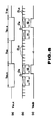
- Fig. 4 shows the cross-section of the photosensors 4 and the first vertical registers 5.
- the CCD1 includes an n-type silicon substrate 11 provided with a p-type well region 12 in which the photosensors 4 and the first vertical registers 5 are formed.
- the photosensor 4 is constituted by a photodiode which is formed by an n-type impurity region 13 in the p-type well region 12 and into which the radiation light is incident via an opening 15 defined between polysilicon layers 14 formed on the substrate surface.
- a sensor gate 16 is also formed on the substrate surface.
- the CCD imager 1 has a vertical overflow drain structure as the structure for draining unnecessary electrical charges. More specifically, the n-type silicon substrate 11 represents an overflow drain and the p-type well region 12 an overflow barrier. Thus an electronic shuttering operation is achieved by raising the substrate voltage V sub applied to the n-type silicon substrate 11. Above all, it becomes possible to suppress the blooming by performing the electronic shuttering operation during the high transfer rate transfer operation, as will be described subsequently.
- the first register 5 is able to transfer electrical charges by a buried channel region 18 on the top of a second p-type well region 17, designed for preventing smearing, with the polysilicon layer 14 as the transfer electrode 14.
- the buried channel region 18 faces the substrate surface and is separated from the remaining vertical columns by channel stop regions 19. It is a region 20 which is disposed below the polysilicon layer 14 and which is spaced apart from the n-type impurity region 13 that acts as a readout gate.
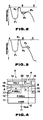
- Figs. 2 and 3 are charts showing the potential energies along a line A-B-C in Fig. 4, wherein Fig. 2 shows the state of electron storage and Fig. 3 the state of electron draining.
- a point P3 by the n-type impurity region 13 represents a potential well.
- a potential barrier is formed at each of a point P4 by the p-type well region 12 and a point P2 by the readout gate and electrical charges are stored at the side of the point P3 of the n-type impurity region 13.
- Reading is performed with the point P2 at the readout gate being lowered by the high potential V H and with the electrical charges thus flowing from the point P3 of the n-type impurity region 13 towards a point P1 of the buried channel region 18. Meanwhile, charge transfer is effected by the potentials at the points P2 and P1 being changed at the required driving periods by the polysilicon layer 14 to which a low potential V L and an intermediate potential V M are supplied.
- Fig. 3 shows the potential state during draining, that is, during electronic shuttering.
- the operation of the CCD1 of the present illustrative embodiment is hereinafter explained by referring to Fig. 5, wherein the signal (a) shows a vertical blanking period T BLK and an image period T VD , the signal (b) a vertical drive pulse of the CCD and the signal (c) a substrate voltage V sub .
- readout pulses ⁇ R are applied to read out the signal charges in the photosensor 4 into the first vertical register 5.
- the substrate voltage V sub is reset to its original voltage, so that the photosensor 4 is again in the charge storage state.
- the sensitivity is lowered by an amount corresponding to the failure to store the charges during the high transfer rate transfer period t2, such lowering in sensitivity is in the order only of several percent.
- the photosensors 4 are brought to a state of not storing electrical charges during the high transfer rate transfer within the vertical blanking period to prevent the occurrence of flaws, such as white-tinted vertical streaks, due to the above mentioned blooming.
- a transverse or horizontal overflow drain may also be operated during the high transfer rate transfer of the electrical charges.
- the potential well of the photosensor may be increased in depth, and/or the barrier of the readout gate may also be increased in height to achieve the same effects.
Landscapes
- Engineering & Computer Science (AREA)
- Physics & Mathematics (AREA)
- Power Engineering (AREA)
- Multimedia (AREA)
- Signal Processing (AREA)
- Electromagnetism (AREA)
- Condensed Matter Physics & Semiconductors (AREA)
- General Physics & Mathematics (AREA)
- Computer Hardware Design (AREA)
- Microelectronics & Electronic Packaging (AREA)
- Transforming Light Signals Into Electric Signals (AREA)
- Solid State Image Pick-Up Elements (AREA)
Applications Claiming Priority (2)
| Application Number | Priority Date | Filing Date | Title |
|---|---|---|---|
| JP1132168A JPH02309877A (ja) | 1989-05-25 | 1989-05-25 | 固体撮像装置 |
| JP132168/89 | 1989-05-25 |
Publications (3)
| Publication Number | Publication Date |
|---|---|
| EP0399551A2 true EP0399551A2 (fr) | 1990-11-28 |
| EP0399551A3 EP0399551A3 (fr) | 1991-04-10 |
| EP0399551B1 EP0399551B1 (fr) | 1997-04-23 |
Family
ID=15074956
Family Applications (1)
| Application Number | Title | Priority Date | Filing Date |
|---|---|---|---|
| EP90109982A Expired - Lifetime EP0399551B1 (fr) | 1989-05-25 | 1990-05-25 | Méthode pour commander un capteur d'images à CCD du type à transfert de trame interligne |
Country Status (4)
| Country | Link |
|---|---|
| US (1) | US5426317A (fr) |
| EP (1) | EP0399551B1 (fr) |
| JP (1) | JPH02309877A (fr) |
| DE (1) | DE69030526T2 (fr) |
Cited By (1)
| Publication number | Priority date | Publication date | Assignee | Title |
|---|---|---|---|---|
| EP0601638A1 (fr) * | 1992-12-09 | 1994-06-15 | Koninklijke Philips Electronics N.V. | Dispositif à couplage de charge |
Families Citing this family (11)
| Publication number | Priority date | Publication date | Assignee | Title |
|---|---|---|---|---|
| BE1007803A3 (nl) * | 1993-11-26 | 1995-10-24 | Philips Electronics Nv | Beeldopneemapparaat. |
| US5900654A (en) * | 1995-07-17 | 1999-05-04 | Spratt; James P. | Radiation hardened charge coupled device |
| US5900769A (en) * | 1995-10-04 | 1999-05-04 | Nec Corporation | Two-dimensional CCD having storage cells for withdrawing charge packets from transfer channels during horizontal scan periods |
| JP3598648B2 (ja) * | 1996-04-02 | 2004-12-08 | ソニー株式会社 | 電荷転送素子及び電荷転送素子の駆動方法 |
| US5872371A (en) * | 1997-02-27 | 1999-02-16 | Eastman Kodak Company | Active pixel sensor with punch-through reset and cross-talk suppression |
| US6778214B1 (en) * | 1998-03-04 | 2004-08-17 | Fuji Photo Film Co., Ltd. | Charge generation of solid state image pickup device |
| JP4450941B2 (ja) * | 2000-04-12 | 2010-04-14 | 富士通マイクロエレクトロニクス株式会社 | 固体撮像素子、画像処理装置及び画像処理方法 |
| US7508432B2 (en) * | 2006-07-19 | 2009-03-24 | Eastman Kodak Company | CCD with improved substrate voltage setting circuit |
| US7834894B2 (en) * | 2007-04-03 | 2010-11-16 | Lifetouch Inc. | Method and apparatus for background replacement in still photographs |
| US8724003B2 (en) | 2012-08-14 | 2014-05-13 | Truesense Imaging, Inc. | Multimode interline CCD imaging methods |
| US9979905B2 (en) | 2015-11-17 | 2018-05-22 | Microsoft Technology Licensing, Llc. | Multimode photosensor |
Citations (5)
| Publication number | Priority date | Publication date | Assignee | Title |
|---|---|---|---|---|
| US4447735A (en) * | 1980-12-19 | 1984-05-08 | Matsushita Electric Industrial Co., Ltd. | Charge-coupled type solid-state image sensor |
| FR2537812A1 (fr) * | 1982-12-10 | 1984-06-15 | Thomson Csf | Procede de reglage du niveau de signal dans un dispositif photosensible a transfert de charge et dispositif pour sa mise en oeuvre |
| US4498013A (en) * | 1981-03-30 | 1985-02-05 | Matsushita Electric Industrial Co., Ltd. | Solid state image sensor exhibiting reduced image smearing effects |
| EP0174133A2 (fr) * | 1984-08-27 | 1986-03-12 | Sharp Kabushiki Kaisha | Capteur d'images à l'état solide |
| WO1988000759A1 (fr) * | 1986-07-24 | 1988-01-28 | Eastman Kodak Company | Obturateur electronique pour capteur d'images utilisant des photodiodes |
Family Cites Families (6)
| Publication number | Priority date | Publication date | Assignee | Title |
|---|---|---|---|---|
| JPS5919480A (ja) * | 1982-07-26 | 1984-01-31 | Olympus Optical Co Ltd | 固体撮像装置 |
| JPS5928772A (ja) * | 1982-08-11 | 1984-02-15 | Sony Corp | 固体撮像装置の駆動方法 |
| JPS6157181A (ja) * | 1984-08-28 | 1986-03-24 | Sharp Corp | 固体撮像装置 |
| EP0178664B1 (fr) * | 1984-10-18 | 1992-08-05 | Matsushita Electronics Corporation | Dispositif détecteur d'image du type à l'état solide et méthode pour sa fabrication |
| JPS62269357A (ja) * | 1986-05-19 | 1987-11-21 | Sony Corp | 固体撮像装置 |
| US4875100A (en) * | 1986-10-23 | 1989-10-17 | Sony Corporation | Electronic shutter for a CCD image sensor |
-
1989
- 1989-05-25 JP JP1132168A patent/JPH02309877A/ja active Pending
-
1990
- 1990-05-25 DE DE69030526T patent/DE69030526T2/de not_active Expired - Fee Related
- 1990-05-25 EP EP90109982A patent/EP0399551B1/fr not_active Expired - Lifetime
-
1994
- 1994-01-21 US US08/185,231 patent/US5426317A/en not_active Expired - Fee Related
Patent Citations (5)
| Publication number | Priority date | Publication date | Assignee | Title |
|---|---|---|---|---|
| US4447735A (en) * | 1980-12-19 | 1984-05-08 | Matsushita Electric Industrial Co., Ltd. | Charge-coupled type solid-state image sensor |
| US4498013A (en) * | 1981-03-30 | 1985-02-05 | Matsushita Electric Industrial Co., Ltd. | Solid state image sensor exhibiting reduced image smearing effects |
| FR2537812A1 (fr) * | 1982-12-10 | 1984-06-15 | Thomson Csf | Procede de reglage du niveau de signal dans un dispositif photosensible a transfert de charge et dispositif pour sa mise en oeuvre |
| EP0174133A2 (fr) * | 1984-08-27 | 1986-03-12 | Sharp Kabushiki Kaisha | Capteur d'images à l'état solide |
| WO1988000759A1 (fr) * | 1986-07-24 | 1988-01-28 | Eastman Kodak Company | Obturateur electronique pour capteur d'images utilisant des photodiodes |
Cited By (1)
| Publication number | Priority date | Publication date | Assignee | Title |
|---|---|---|---|---|
| EP0601638A1 (fr) * | 1992-12-09 | 1994-06-15 | Koninklijke Philips Electronics N.V. | Dispositif à couplage de charge |
Also Published As
| Publication number | Publication date |
|---|---|
| EP0399551A3 (fr) | 1991-04-10 |
| EP0399551B1 (fr) | 1997-04-23 |
| DE69030526T2 (de) | 1997-08-07 |
| US5426317A (en) | 1995-06-20 |
| DE69030526D1 (de) | 1997-05-28 |
| JPH02309877A (ja) | 1990-12-25 |
Similar Documents
| Publication | Publication Date | Title |
|---|---|---|
| US4322753A (en) | Smear and/or blooming in a solid state charge transfer image pickup device | |
| US8253833B2 (en) | Solid-state imaging device driving method | |
| KR100633493B1 (ko) | 고체 촬상 장치 | |
| US5896172A (en) | Method of operating a CCD imager suitable for the implementation of such a method | |
| US4697200A (en) | Field storage drive in interline transfer CCD image sensor | |
| US5703386A (en) | Solid-state image sensing device and its driving method | |
| JPH10150183A (ja) | 固体撮像装置およびその駆動方法並びにカメラ | |
| US5432551A (en) | Interline transfer image sensor | |
| US5426317A (en) | Frame interline transfer CCD imager | |
| CA1193711A (fr) | Senseur d'images a semiconducteurs | |
| US4577233A (en) | Solid image-pickup device | |
| EP1717860B1 (fr) | Capteur d'image à l'état solide | |
| US4663771A (en) | Solid state image pickup device in which the transfer gate areas are supplied with negative voltage during the vertical transfer period and light receiving period but not when the positive readout pulse period is applied | |
| US6760073B1 (en) | Solid-state image sensor | |
| US4605862A (en) | Solid state image pickup apparatus | |
| JPH04268764A (ja) | 固体撮像装置 | |
| US7315328B1 (en) | Solid-state image sensor device and driving method | |
| JPH0446504B2 (fr) | ||
| US4837629A (en) | Image pickup method using a CCD-type solid state image pickup device with charge dissipation | |
| US4532549A (en) | Solid-state imaging device with high quasi-signal sweep-out efficiency and high signal charge transfer efficiency | |
| US6628332B1 (en) | Interline transfer type imaging device suitable for producing high resolution still images | |
| US5283633A (en) | Solid state image pickup device in which picture elements of green are generated in vertical charge transfer paths | |
| JP2987844B2 (ja) | 固体撮像装置及びその駆動方法 | |
| JP2001177769A (ja) | 固体撮像素子の駆動方法 | |
| JPS6089177A (ja) | 撮像素子 |
Legal Events
| Date | Code | Title | Description |
|---|---|---|---|
| PUAI | Public reference made under article 153(3) epc to a published international application that has entered the european phase |
Free format text: ORIGINAL CODE: 0009012 |
|
| AK | Designated contracting states |
Kind code of ref document: A2 Designated state(s): DE FR GB |
|
| PUAL | Search report despatched |
Free format text: ORIGINAL CODE: 0009013 |
|
| AK | Designated contracting states |
Kind code of ref document: A3 Designated state(s): DE FR GB |
|
| 17P | Request for examination filed |
Effective date: 19911010 |
|
| 17Q | First examination report despatched |
Effective date: 19931230 |
|
| GRAG | Despatch of communication of intention to grant |
Free format text: ORIGINAL CODE: EPIDOS AGRA |
|
| GRAH | Despatch of communication of intention to grant a patent |
Free format text: ORIGINAL CODE: EPIDOS IGRA |
|
| GRAH | Despatch of communication of intention to grant a patent |
Free format text: ORIGINAL CODE: EPIDOS IGRA |
|
| GRAA | (expected) grant |
Free format text: ORIGINAL CODE: 0009210 |
|
| STAA | Information on the status of an ep patent application or granted ep patent |
Free format text: STATUS: THE PATENT HAS BEEN GRANTED |
|
| AK | Designated contracting states |
Kind code of ref document: B1 Designated state(s): DE FR GB |
|
| PGFP | Annual fee paid to national office [announced via postgrant information from national office to epo] |
Ref country code: FR Payment date: 19970513 Year of fee payment: 8 |
|
| PGFP | Annual fee paid to national office [announced via postgrant information from national office to epo] |
Ref country code: GB Payment date: 19970516 Year of fee payment: 8 |
|
| REF | Corresponds to: |
Ref document number: 69030526 Country of ref document: DE Date of ref document: 19970528 |
|
| PGFP | Annual fee paid to national office [announced via postgrant information from national office to epo] |
Ref country code: DE Payment date: 19970530 Year of fee payment: 8 |
|
| ET | Fr: translation filed | ||
| PLBE | No opposition filed within time limit |
Free format text: ORIGINAL CODE: 0009261 |
|
| 26N | No opposition filed | ||
| PG25 | Lapsed in a contracting state [announced via postgrant information from national office to epo] |
Ref country code: GB Free format text: LAPSE BECAUSE OF NON-PAYMENT OF DUE FEES Effective date: 19980525 |
|
| PG25 | Lapsed in a contracting state [announced via postgrant information from national office to epo] |
Ref country code: FR Free format text: LAPSE BECAUSE OF NON-PAYMENT OF DUE FEES Effective date: 19980531 |
|
| GBPC | Gb: european patent ceased through non-payment of renewal fee |
Effective date: 19980525 |
|
| PG25 | Lapsed in a contracting state [announced via postgrant information from national office to epo] |
Ref country code: DE Free format text: LAPSE BECAUSE OF NON-PAYMENT OF DUE FEES Effective date: 19990302 |
|
| REG | Reference to a national code |
Ref country code: FR Ref legal event code: ST |